2D Magnetic Heterostructures: Spintronics and Quantum Future
Abstract
The discovery of two-dimensional (2D) magnetism within atomically thin structures derived from layered crystals has opened up a new realm for exploring magnetic heterostructures. This emerging field provides a foundational platform for investigating unique physical properties and exquisite phenomena at the nanometer and molecular/atomic scales. By engineering 2D interfaces using physical methods and selecting interlayer interactions, we unlock the potential for extraordinary exchange dynamics. This potential extends to high-performance and high-density magnetic memory applications, as well as future advancements in neuromorphic and quantum computing. This review delves into recent advances in 2D magnets, elucidates the mechanisms behind 2D interfaces, and highlights the development of 2D devices for spintronics and quantum information. Particular focus is placed on 2D magnetic heterostructures with topological properties, promising for a resilient and low-error information system. Finally, we discuss the trends of 2D heterostructures for future electronics, considering the challenges and opportunities from physics, material synthesis, and technological prospective.
I Introduction
The advent of 2D van der Waals (vdW) materials1; 2; 3; 4 has sparked a revolution in the field of magnetism, primarily due to the substantial influence of the dimensionality confinement and size effects upon spin textures and dynamics, e.g., quantum fluctuations. These 2D layered magnetic materials (2D magnets) have garnered immense attention, driven by both their fundamental significance and facile integration into multi-layer heterostructures. Ever since the experimental discovery of 2D magnets with intrinsic magnetism in 2017, like CrI3 and Cr2Ge2Te6 5; 6, 2D magnets family has expanded significantly over the years. Unlike ultrathin film systems grown on a substrate (e.g., CoFeB/MgO), these 2D magnets possess a naturally layered structures, high crystallinity, and weak coupling to any transferred substrate. Furthermore, the reduced coordination effects7, e.g., finite size effect, seen in ultrathin films are less pronounced in these layered magnets, thanks to their weak interlayer interactions. Consequently, these 2D magnets serve as tailored testbeds for exploring the pure dimensional transition of magnetism from 3D to 2D. Additionally, these magnets exhibit high responsivities to external stimuli, such as gate voltage, molecule adsorption, and neighboring materials. The unique controllability of magnetism by electric ways opens up possibilities for creating heterostructures and devices for applications in spintronics and memory technology.
However, it is worth noting that the magnetic properties of individual 2D magnets are typically monotonous and imperfect, which poses significant limitations for further applications. Therefore, an effective strategy involves modulation of their magnetism through heterostructure construction, which can tune the electronic band structures of 2D magnets via interfacial interactions. Artificial structures can be assembled to manipulate and enhance their magnetism through magnetic coupling. Furthermore, these 2D magnets can be harnessed to induce valley polarization and spin splitting in many nonmagnetic 2D materials, such as monolayer graphene8 and topological insulators9; 10; 11.
Based on these magnetic heterostructures, 2D spintronics is an emerging field to realize devices such as magnetic tunneling junctions (MTJ), spin field-effect transistors and memoristors12; 13; 14; 15. 2D spintronics has unwrapped innovation and compelling opportunities which not only improve their performance but also diversify the functionality of electronic devices. For example, imprinted magnetic skyrmions can only exist at 2D interfaces16, which can be used as parallel information storage channels. When combined with electrical control, switch of skyrmion on/off states can be realized17; 18. Besides, 2D magnetic heterostructures for unconventional computing is an emerging field. One examples is for neuromorphic computing, which traditionally employs 3D bulk materials or nonlayered thin films, and thus the resulting device size is either difficult to scale down for high density integration or suffering from lattice mismatch problems. The emergence of 2D magnets offers a promising solution, as evidenced by the surge of reported 2D heterostructures functioning as neuromorphic computing devices19; 20, as well as using skyrmions21; 22; 23. Another area is for quantum computing, concepts such as using 2D magnetic heterostructures with superconductors towards topological superconductivity24; 25 and skyrmion qubits26; 27, with scalibility, offer easy electric control and new functionality. In this review, we will first discuss the large family of existing 2D mangets, including ferromagnet, antiferromagnet, and multiferroics, then discuss the multifunctionality in 2D magnetic heterostructures. Based on these heterostructures, 2D devices for spintronics will be discussed, with a targeting for applications in high-performance and high-density magnetic memory, as well as neuromorphic and quantum computing.
II Library of 2D Magnets
The hallmark of 2D magnetism is the existence of an ordered arrangement of magnetic moments over macroscopic length scales at any finite temperature, with a spontaneous breaking of time-reversal symmetry. Since first discovery in 2017, a rich collection of layered magnetic materials covering a wide spectrum of magnetic properties has been reported, as shown in Figure 1. Many of these materials are semiconductors with bandgaps covering the near-infrared to the ultraviolet spectral range, whereas a few are metallic.
Ferromagnetic (FM) order exists in both layered transition metal halides and chalcogenides, when the exchange interactions favor both intralayer and interlayer parallel spin alignments. The Curie temperature is known as the temperature above which the material undergoes a magnetic transition from a ferromagnet to a paramagnet. While antiferromagnetic (AFM) materials have a rich variety of magnetic orders, they can be broadly divided into two types: those with intralayer FM order and interlayer AFM order, and others with intralayer AFM order. Antiferromagnets (antiferros) are magnetic ordered, yet with zero magnetization, making them immune to external field perturbations. Their AFM order is established by the exchange interactions between the spins, which produces an exchange field in the order of to T and give rise to a THz spin precession frequency. In the following, we discuss some magnetic materials under extensive studies, with physical properties promising for device design.
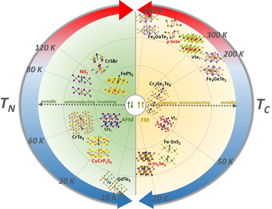
Multilayer CrI3 exhibits interlayer AFM behavior, while monolayers display FM ordering. The atomically thin CrI3 flakes were successfully prepared by mechanical exfoliation, and the monolayer FM properties were subsequently demonstrated using a low-temperature microscopic magneto-optical Kerr effect (MOKE) measurement setup6. The transition temperature for monolayer was measured at 45 K, slightly lower than the bulk of 61 K28; 29. The bilayer CrI3 shows AFM behaviour due to a weak AFM interlayer coupling, which is different from monolayer. The interlayer magnetic coupling can be tuned by external field, either magnetic or electric fields. If an out-of-plane magnetic field is applied, with a field strength of 0.65 T, it can flip the magnetization in one layer and change the bilayer from AFM to FM state. Gate voltage applied through electric way can also help switch CrI3 between FM and AFM states, with more energy-efficiency30.
The intrinsic ferromagnetism in 2D Cr2Ge2Te6 (CGT) layers was reported around the same time as CrI35, and it is also revealed by MOKE microscopy under a small stabilizing magnetic field of 0.075 T. CGT is a FM material with a band gap around 0.8 eV31. Its electrical property was characterized with a two-terminal resistivity of around M at room temperature32, showing the electrically resistive nature. Thus few work can be done to study its transport properties. Additionally, CGT thin layers exhibit a thickness-dependent , from a bilayer value of about 30 K to a bulk limit of 68 K. This thickness dependence of exists also in as-grown thin magnetic films, which shows more pronounced dependence33.
These two materials mentioned above have relatively low , with respect to room-temperature memory device. To market application of 2D magnets in spintronic devices, the emphasis is on developing 2D materials with stable magnetic properties at room temperature. Among all 2D magnets, Fe-based materials usually have higher , e.g. Fe3GeTe2 (FGeT). Its itinerant ferromagnetism was observed to persist down to the monolayer, due to its strong perpendicular magnetic anisotropy (PMA) with a uniaxial magnetocrystalline anisotropy constant =1.46 erg/cm3.34 This anisotropy energy is about two or three orders of magnitude larger than CrI3 (=4.3 erg/cm3 at 50 K)35 and CGT (=1 erg/cm3)36 case. In bulk FGeT, the is K, depending on Fe deficiency. Although this value is diminished in atomically thin FGeT flakes, it can be significantly elevated to reach room temperature by employing liquid gating37, showing electrically tunable nature of these 2D magnetism.
Another example is VSe2, with monolayer grown by molecular beam epitaxy (MBE) method. This material has been shown to maintain its FM ordering at 330 K38. Exceptionally, a recent discovered material Fe3GaTe2 (FGaT), with similar crystal structure to FGeT, exhibits as an above room temperature 2D metallic ferromagnet39. It has been demonstrated a record-high (350-380 K) as well as a robust PMA. These outstanding magnetic properties render Fe3GaTe2 a widely favored material for practical magnetoelectronic and spintronic applications.
Beyond magnetic properties, these 2D magnets also provide a unique platform for the realization of topological magnetic materials, to study the interplay between magnetism and topology. MnBi2Te4 and its derivative compounds have received focused attention recently for their inherent magnetic order and the rich, robust and tunable topological phases11. MnBi2Te4 has an AFM interlayer coupling, while a FM order exists in each single layer, with out-of-plane easy magnetic axis. The interplay between the magnetic structure and the topological nontrivial bands endows the materials with rich topological phases, e.g. quantized anomalous Hall effect above 1.5 K40, which has higher temperature than magnetically doped BST samples41. In odd-layer flakes, quantum anomalous Hall effect was observed with quantized plateaus of Hall resistivity as well as diminishing longitudinal resistance42, absence of any applied magnetic fields. This is extremely promising for low-power devices with dissipationless edge states. These materials and their heterostructures provide a neat, simple and versatile way to fuse topological bands with magnetic order, which are promising to help push quantum anamolous Hall effect towards the liquid nitrogen temperature. Possession of topology contributes to improving the performance of electronic components, by enabling high fault tolerance with topological protection, which is a key factor desired in quantum computing.
Additionally, 2D multiferroic materials are actively studied for their cross-coupling effects. This class of materials exhibit multiple ferroic properties simultaneously, including ferromagnetism, ferroelectricity, and ferroelasticity. Multiferroics hold great promise for the development of innovative, multifunctional devices, with enhanced device performance and scaled down size in vdW case. The discovery of type-II multiferroic order in a single atomic layer of the transition-metal-based layered material NiI2 was reported recently43, which exhibits an inversion-symmetry-breaking magnetic order and directly induces a ferroelectric (FE) polarization. Later, intriguing in-plane electrical and magnetic anisotropies in layered multiferroic CuCrP2S644 has generated much excitement owing to coexsitence of antiferroelectric and antiferromagnetism, along with strong polarization-magnetization coupling. These multiferroics enable magnetization affected by electric field, and vice versa. This functionality has motivated fundamental and applied research in applying multiferroics for voltage controlled magnetic anisotropy, towards low-power switching devices.
Overall, the current main thrusts for 2D magnets search are (1) room-temperature atomically thin magnet, for high-density and high-performance memory; (2) FM or AFM semiconductors with a tunable band gap and a stability, which would be an ideal platform to investigate the magneto-electric coupling between electrons and spin; (3) exotic topological properties, like searching for high-temperature quantum anomalous Hall insulators; (4) large-scale thin films for device integration. Although 2D exfoliated films offer high quality of layers, the limitation on the lateral size normally to hundreds of micrometers still prohibits their applications in the integration level. Efforts are working on to obtain high-quality wafer-scale 2D magnetic heterostructures.
III 2D Magnetic Heterostructures and Their Interface
2D magnetic heterostructure is a material system composed of two or more distinct layers of atomically thin magnetic materials stacked on top of each other. These layers can have different magnetic properties or orientations. The use of 2D magnetic heterostructures is mainly for two purposes. One is to expand the functionality of these structures for both experimental investigations and future practical applications. The other is, the proximity effects within heterostructuers give rise to valuable phenomena that enhance the magnetic properties. When combining with magnetism, the interface has even more intriguing physics and phenomena as shown in Figure 2, compared to the charge-based system.
Firstly, the orbital hybridization at the interface can not only induce the exchange interaction at the interface, but also modify the electronic and magnetic properties in adjacent layers by impacting their band structure and orbital characters. Established orbital hybridization is a new degree of freedom for controlling interfacial Dzyaloshinskii-Moriya interaction (DMI), a short-range anti-symmetric exchange interaction45. Taking CGT/FGeT heterostructure for examples, the topological Hall effect arising from magnetic skyrmions was observed, which are due to interfacial DMI16.
Another proximity effect is exchange coupling, which refers to the interaction between magnetic moment of different layers within the heterostructure. It’s crucial for the applications in magnetic memory and spintronic devices, like spin valve, MTJ and magnetic sensors based on giant magnetoresistance (GMR) or tunneling magnetoresistance (TMR). As reported, large exchange bias observed in a FGeT/antiferro interface46, which is tunable by magnetic field cooling. Antiferro, with zero magnetization, shows robustness against external perturbations and THz fast spin procession. These makes coupling to antiferro materials extremely promising.

Following is lattice perturbation, which distorts the crystal lattice structure at the interface, thus tuning the magnetic behaviours. Examples include applying electric voltages and vertical stacking to form the Moiré lattice47. This can lead to either the control of magnetization or the emergence of new exotic effects like Moiré skyrmions48.
Different from above mechanism, strain effect arises from mechanical deformation, leading to the change of electronic band structures. The methods to induce strain include lattice mismatch, utilization of flexible, patterned, or piezoelectric/FE substrates, as well as an atomic force microscopy tip or even the presence of bubbles at the interface during sample assembly.
Spin-orbit coupling (SOC) refers to the interaction between the spin and orbital angular momentum of electrons across different layers within the heterostructure. This can play an important role when 2D magnet is interfaced with heavy metal element. An example of this is the emergence of skymions in WTe2/FGeT heterostructure49 through SOC coupling. This SOC is also crucial to realize spin-orbit torque (SOT) or spin-transfer torque (STT) in magnetic random-access memory (MRAM).
The last but significant effect is the magnetoelectric effect, which occurs when a FM layer interfaces with a FE or multiferroic layer. The magnetism of the FM material can be switched by the electric polarization in the FE layer, and vice versa. FE control of magnetism is particularly interesting due to its energy-efficient and nonvolatile nature. One example is to use a thin FE polymer to open and close the CGT magnetic loop50.
| Material | Thickness (nm) | Polarization (C/cm2) | Coercive field (MV/cm) | |
|---|---|---|---|---|
| 2D FEs | CuInP2S6 | N/A | 2.55 | 0.077 |
| -In2Se3 | 5 | 2-11 | 0.2 | |
| h-BN | N/A | 0.09 | 2 | |
| Other FEs | HfxZr1-xO2 | 0.5-30 | 5-50 | 1-3 |
| Al | <10 | 100-150 | 3-7 | |
| Al | 500 | >125 | 5-6 | |
| Zn | 500 | 25-100 | 2-3 | |
An alternative promising approach to generate a substantial magnetoelectric effect involves the stacking 2D FM layer with recently emerging fluorite51; 52; 53 and wurtzite FE54; 55; 56 materials. These CMOS-compatible FE materials, such as hafnium-dioxide, zinc-magnesium-oxide, or aluminum-scandium-nitride, offer a unique advantage over conventional perovskites due to their remarkable scalability, while providing very large polarization and coercive fields57. Moreover, fluoride FEs with sub-nm thickness58; 59 and wurtzite FEs with sub-10 nm thickness60 have been demonstrated, and their integration with 2D materials is explored to create novel memory devices are explored61. In comparison to 2D FEs62; 63 as shown in Table 1, these 3D yet atomically thin materials offer one to two orders of magnitude higher polarization, significantly amplifying magnetoelectric effects at the interface with FMs64. Additionally, they boast coercive fields two to three orders of magnitude higher compared to 2D FE counterparts, enabling the attainment of higher switching voltages and improved interstate isolation, which is desirable for memory applications.
The high-quality and seamless 2D interfaces offer a platform for introducing new functionalities into 2D devices, thereby enabling the exploration of novel physics and effects. Of particular interest is the pursuit of ultra-fast, ultra-compact, and energy-efficient spintronics through precise interface engineering. By leveraging the interface, it becomes possible to amalgamate THz spin procession in AFM materials, nonvolatile control via 2D FEs, and scalable configurations into a single device. This development holds significant promise for advancing the field of spintronics in the future.
IV 2D Spintronics
IV.1 Device for Magnetic Memory
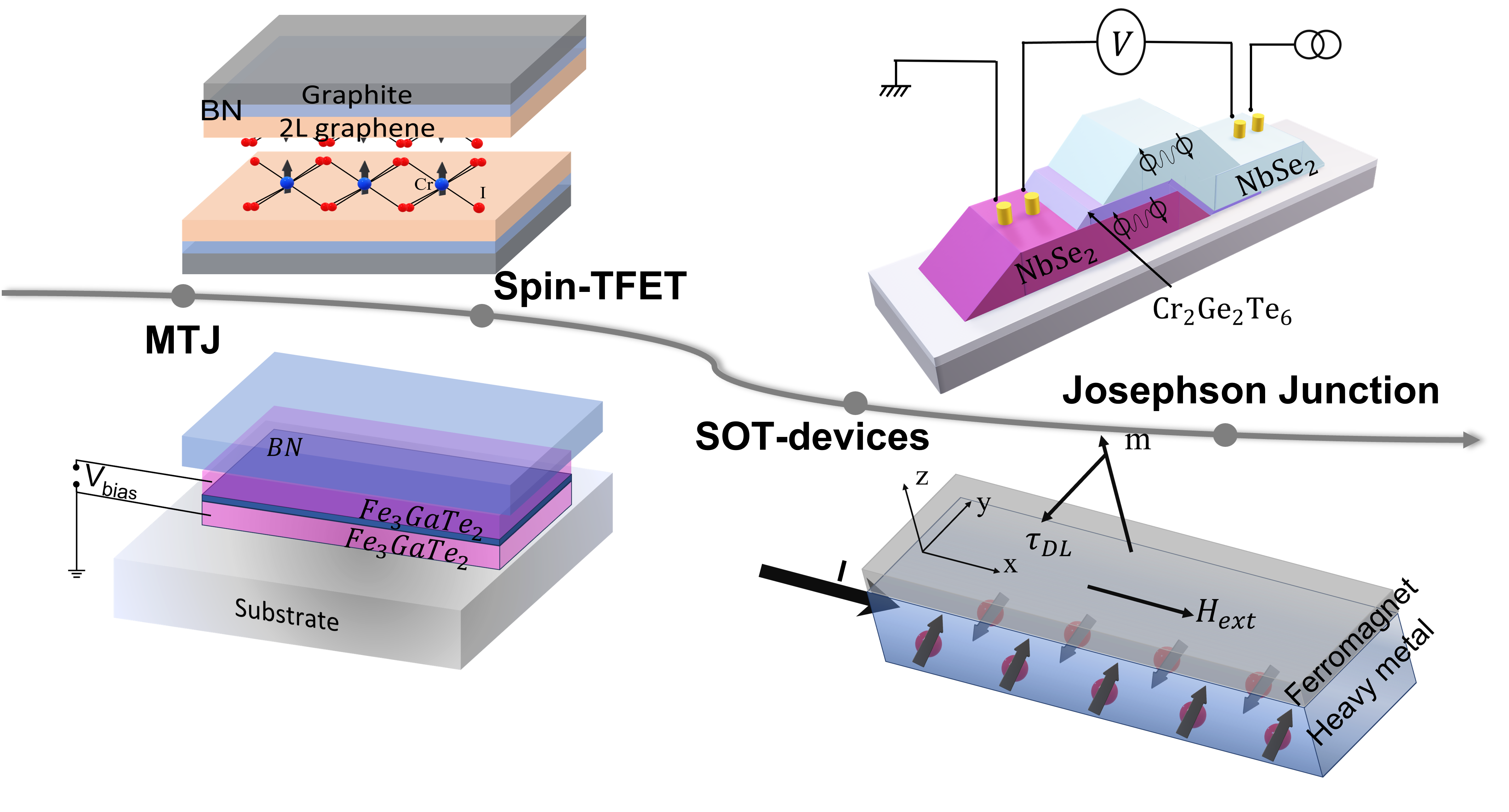
Introducing magnetic elements into memory devices provides substantial advantages, particularly in achieving non-volatile memory functionality. The utilization of 2D magnetic heterostructures, comprised of multiple layers of 2D materials with unique properties, takes these advantages even further. It enhances energy efficiency, boosts data storage density, and enriches the range of functionalities achievable within a single memory device, as shown in Figure 3.
MTJ is a fundamental component in modern memory devices. It consists of two FM layers separated by a thin insulating barrier. The core principle governing MTJ operation is the TMR effect, wherein the electrical resistance of the junction changes based on the relative alignment of magnetization in the two FM layers. In contrast to traditional bulk ferros such as Fe3O4 and Co, employing atomically thin layered magnets for MTJs offers the potential to significantly enhance their TMR, since TMR heavily depends on interface quality. Additionally, this approach relaxes the stringent lattice-matching requirements associated with epitaxy growth and enables high-quality integration of dissimilar materials with atomically sharp interfaces.
Among the existing 2D magnets, CrI3 stands out due to its layered AFM ordering and relatively electrically insulating properties, making it a desirable choice as tunnel barrier in MTJs. One spin-filter MTJ design involves a heterostructure consisting of h-BN encapsulated graphene/CrI3/graphene layers65. This device demonstrated remarkable TMR values of 530%, 3200%, and 19,000% for bilayer, trilayer, and four-layer CrI3 structures, respectively. The highest value of the four-layer structure greatly exceeds typically achieved in conventional bulk material MTJs66; 67. While MTJs based on CrI3 exhibit promising properties in TMR, it’s crucial to acknowledge their operational constraints - cryogenic low temperature for operation and need of magnetic fields. In response, ongoing research focuses on advancing MTJs by employing materials suitable for room-temperature operation. A notable candidate is FGaT, which boasts a high of 380 K, as well as operation temperature above room temperature. This characteristic overcomes the limitation, greatly facilitating the realization of practical spintronic devices. A room-temperature MTJ based on a FGaT/WSe2/FGaT heterostructure was successfully demonstrated68, showing significant TMR of 85% at room temperature.
Spin field-effect transistor (Spin-FET) is a new type of spintronics device towards non-volatile memory. This device utilizes the spin, rather than charge, in the flow of electrical current, which could potentially offer non-volatile data storage and improved performance compared with traditional FETs. The application of a magnetic tunnel barrier in MTJ can be extended to Spin-FETs, leading to a noval device - the spin tunnel FET, e.g. dual-gated graphene/CrI3/graphene tunnel junctions69, with similar structure as spin-filter MTJs. This device achieves an impressive high-to-low conductance ratio of nearly 400% by electrical modulation of magnetization configurations. However, it shares a common constraint with CrI3-based MTJs, requiring low operational temperatures and magnetic fields. Despite these challenges, the search for high-temperature semiconducting magnets holds the key to advancing the development of this device, potentially overcoming existing limitations and paving the way for future applications.
Utilizing SOC, SOT devices are engineered to manipulate the magnetization of a magnetic layer by an spin-polarized current. Compared to traditional STT devices, SOT devices are anticipated to offer superior performance like easy stacking, operation in sub-ns writing and reading speed. Typically, a SOT device comprises two key components: a FM layer and a non-magnetic heavy metal (HM) layer. SOT efficiency heavily relies on the interface quality. Thus, 2D magnets can be promising building blocks for SOT devices, like CGT, CrI3, and FGeT with intrinsic PMA. Even in monolayer form, these materials maintain their PMA, making them highly responsive to external stimuli. In the initial designs of 2D magnetic SOT devices, structures like Pt/FGeT70 and Ta/CGT71 were featured, showing significant improvements in SOT switching efficiency with the incorporation of 2D FM materials. Creating all-vdW heterostructures can further enhance the switching efficiency. For instance, a FGeT/WSe2 heterostructure was realized72, achieving a remarkably low switching current density of 3.90 A/cm2 at 150 K, which is comparable or even better to that of conventional thin films system73; 74. Recent research efforts have been directed towards achieving reliable vdW SOT operation at room temperature. One work75 incorporates high FGaT to achieve room temperature operation, with a FGaT/Pt bilayer structure. Currently, this approach still needs a high switching current density of 1.3107 A/cm2. Another notable approach involves a wafer-scale FGeT/Bi2Se3 layered heterostructure76, where the topological insulator Bi2Se3 plays a crucial role in raising the TC of FGeT to room temperature through exchange coupling. This approach has yielded promising results, including a high damping-like SOT efficiency of 2.69 and a notably low switching current of 2.2 106 A/cm2 at room temperature. This development marks a significant step toward practical SOT devices for real applications.
Apart from conventional memory, Josephson junction (JJ) combines the quantum phenomena with memory device technology, opening the door to the development of superconducting Random Access Memories (RAMs)77. JJs are typically composed of two superconductors (SCs) separated by a thin insulating or non-superconducting barrier. JJ based on 2D ferro/SC heterostructure presents unique opportunity to explore the interaction between superconductivity and ferromagnetism. For instance, one approach involves constructing a JJ by introducing a few-layer FM insulator, CGT, between two layers of SCs NbSe278. This JJ demonstrates a hysteresis behavior in the critical current, which is induced by the remanence of the magnetic barrier. Following this, another lateral JJ emerged, composed of a FGeT, laterally interconnected between two layered spin-singlet SCs NbSe279. This SC/ferro/SC heterostructure successfully sustains skin Josephson supercurrents with a remarkable long-range reach over 300 nanometers (nms).
IV.2 2D Magnetic Heterostructures for Neuromorphic Computing
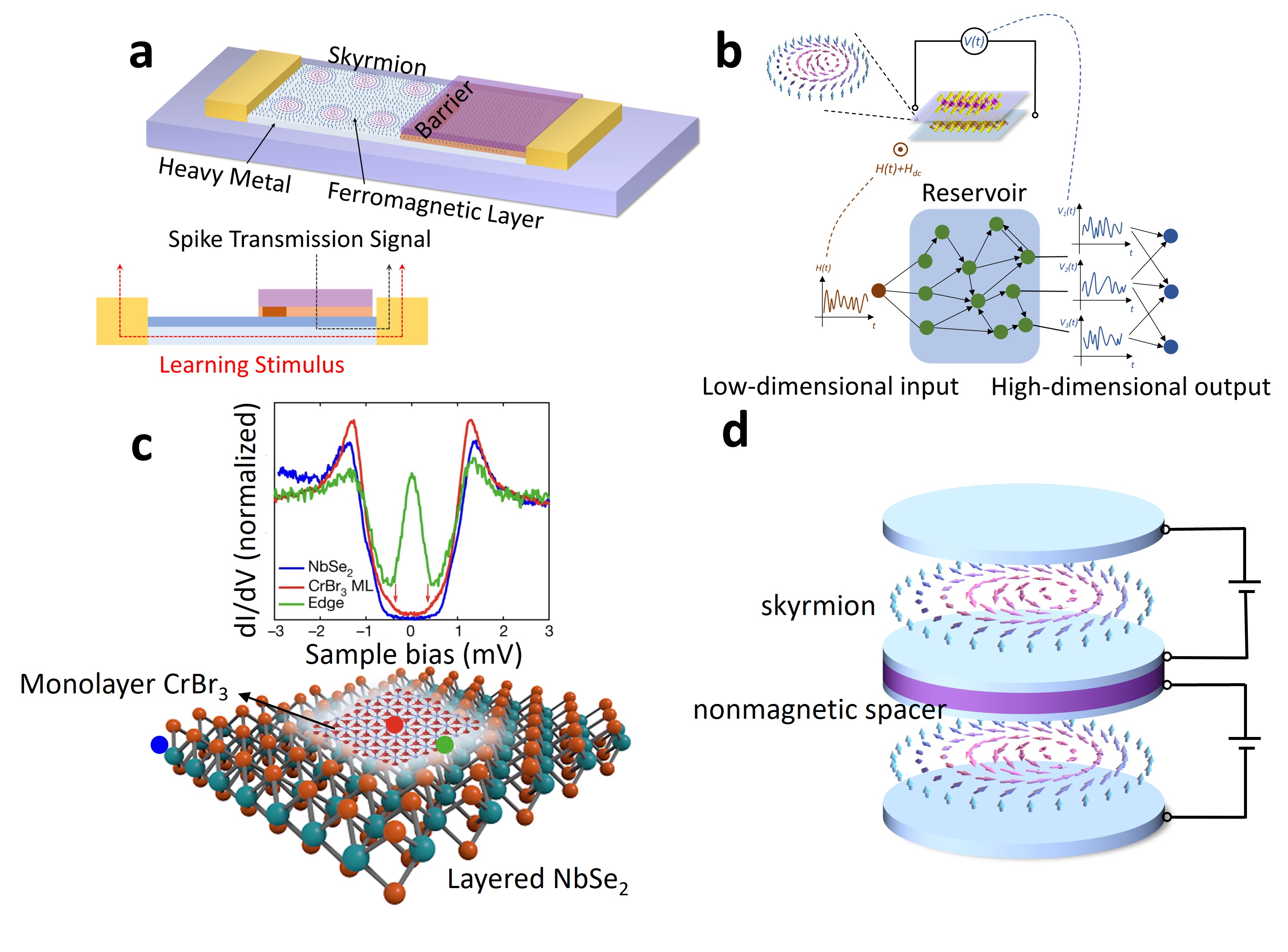
Neuromorphic computing is an emerging field of artificial intelligence that seeks to design computer systems inspired by the human brain’s neural architecture. Owing to the atomic thickness, dangling-bond-free surfaces and high mechanical robustness, 2D materials and heterostructures are extensively investigated for neuromorphic computing devices, showing great promise for high-performance artificial neurons and synapses80; 81; 82; 83; 84. The integration of magnetic elements within 2D materials to form 2D magnetic heterostructures takes this field a step further. These magnetic elements provide non-volatility, longevity, and high-density information storage capabilities. Furthermore, 2D magnetic heterostructures have the capability to generate skyrmions16; 49, which are topological spin structures with unique topology towards more compact, energy-efficient, fault-tolerant and resilient neuromorphic devices23; 22; 85. Figure 4a schematics an artificial synapse device concept based on skyrmions86. The primary component of the device is a 2D ferro/heavy metal heterostructrue, which forms a nanotrack for skyrmions motion. The system replicating the operations of biological neurons and synapses through the following processes: in spike transmission mode, the pre-neuron’s spike is modulated by the synaptic device’s weight (reading through magnetoresistance), leading to the generation of a post-synaptic spike current. During the learning phase, a bidirectional charge current through the heavy metal layer injects a vertical spin current in FM layer, driving the skyrmions into (or out of) the postsynaptic region. This dynamic process effectively adjusts the synaptic weight, closely mirroring the potentiation and depression mechanisms observed in biological synapses. Additionally, the resolution of the synaptic weight can be adjusted based on the nanotrack width and the skyrmion size, which enriches the flexibility and tunibility of the skyrmion-based synapse. Another example for the application of 2D skyrmions is the reservoir computing22, a framework derived from recurrent neural network theory. The essence of reservoir computing is the nonlinear transformation of input into high-dimensional outputs. A physical system capable of implement the reservoir part should possess both complex nonlinearity and memory effect (or equally hysteresis) while also exhibiting short-term properties87; 88; 89. Thus, magnetic skyrmions emerge as a promising candidate. In Figure 4b, 2D skyrmion system performs as the "resvervoir part", nonlinearly converting the one-dimensional time-series input to the linearly independent -dimensional time-series outputs . This design provides a guideline for developing energy-saving and high-performance skyrmion neuromorphic computing devices.
V 2D Heterostructures for Quantum Computing
2D magnetic heterostructures hold promise for quantum computing due to their unique electronic properties, controllability, and potential for creating novel quantum states. These interfaces can give rise to emergent quantum phenomena, broadening the horizons for quantum information processing. Notably, topological quantum computing benefits significantly from the topological protection and qubit safeguarding that 2D magnet/magnetic heterostructure can offer. An illustrative example is the observation of 2D topological superconductivity within vdW heterostructures that combine the ferro CrBr3 with the SC NbSe225. As Figure 4c shows, the monolayer CrBr3 island was grown on the NbSe2 layer. The spectrum was characterized at different sites of this structure: NbSe2 substrate (blue), the middle of the CrBr3 island (red) and the edge of the CrBr3 (green). Among them, a peak of conductance localized at can be clearly seen for the edge of magnetic island, which exhibits as a hallmark of topological superconductivity for this structure. Furthermore, owing to the 2D layered structure, these edge modes can be readily accessed and manipulated using various external stimuli, including electrical, mechanical, and optical methods. This feature enhances the promise of these heterostructures for integration into components of topological quantum computing systems.
Another application of 2D magnetic heterostructures in quantum computing is the implementation of skyrmion qubit. Unlike other proposed qubit systems such as trapped atoms, quantum dots, and photons, magnetic skyrmions offer a topologically protected structure that shows promise in resisting external perturbations and faults. Moreover, skyrmion qubits hold additional potential in addressing challenges related to control and scalability, further enhancing their viability in quantum information processing. In Figure 4d, a skyrmion qubit concept is illustrated, utilizing a bilayer magnetic materials platform26. In this setup, quantum information is stored within the quantum degree of helicity, and the logical states can be dynamically adjusted through the manipulation of electric and magnetic fields.
VI Conclusions and perspectives
For decades, 2D magnetism has been a captivating subject, especially in the context of the Mermin-Wagner-Hohenberg (MWH) theorem, which predicts that thermal fluctuations will disrupt long-range magnetic order in 2D systems at any finite temperature, following the isotropic Heisenberg model. Extensive theoretical and experimental studies have been undertaken to unravel causes of long-range ordering in 2D systems. Beyond magnetization, other physical properties, including polarization, that may exhibit potential long-range order within 2D systems hold the promise of pushing the limits of Moore’s law. The inherent atomic-layer cleavability and magnetic anisotropy of 2D magnets may help mitigate spin fluctuations in the face of short-range interactions, thus paving the way for the emergence of 2D magnetism. While the duality in electromagnetism remains a profound aspect of fundamental physics, the recent discovery of 2D multiferroics further reinforces this concept, as ferroelectricity is analogous to ferromagnetism. These discoveries pose thought-provoking questions, such as the existence of an electric counterpart to the MWH theorem. Considering dipole-dipole interactions, the absence of polarization becomes a relevant consideration. Much like magnetic skyrmions are topological whirls in magnetization, one might comtemplate the existence of a FE equivalent.
The allure of 2D magnets extends beyond fundamental physics and into the realm of novel device fabrication. Significant progress has been made in comprehending their fundamental properties, and the demonstration of devices is in its nascent stages. We have witnessed the expansion of the materials library and glimpsed the potential device functionalities. However, achieving integration of these materials into functional devices requires large-area wafer-scale materials growth. Encouraging strides have been made through techniques such as MBE and atomic layer deposition (ALD), e.g. large-scale monolayer CrBr3 with MgO as a passivation layer from ALD 90 and wafer-scale FGeT on Bi2Te3 from MBE20. Challenges still persist at the device level, particularly in advancing dielectric and contact interfaces. The self-passivated nature of monolayer 2D magnets will necessitate seeding for the deposition of dielectrics through methods like ALD. It may lead to non-ideal interfaces, limiting device performance compared to the best laboratory data that employs crystalline 2D insulators like h-BN. Similar challenges are encountered with electrical contacts, as they only partially conform to industry specifications and have not yet reached the level of readiness required for manufacturing. Addressing these crucial manufacturing bottlenecks will pave the way for a significant enhancement in chip functionality, heralding a new era of 2D magnet applications characterized by increased device complexity.
Moreover, in the context of neuromorphic computing, a fundamental challenge lies in improving the endurance of resistance switching. Achieving material uniformity is essential to create massively connected device arrays capable of mimicking the hyper-connectivity and efficiency of the brain. Computational methods will be employed to guide experimental studies and optimize memristive devices for maximum performance.
For using 2D magnetic heterostructures in topological quantum computing, quantum states can benefit from topological protection, safeguarding qubits against external perturbations and errors, in contrast to standard quantum computing. Efforts in topological superconductivity and skyrmion qubits present a unique opportunity to explore the interplay between topology, magnetism, and electronic properties, potentially yielding new discoveries and insights in physics, as well as paving the way for future quantum computing devices.
References
References
- Chen et al. (2016) X. Chen, L. Wang, Y. Wu, H. Gao, Y. Wu, G. Qin, Z. Wu, Y. Han, S. Xu, T. Han, et al., 2D Materials 3, 015012 (2016).
- Wu et al. (2016) Y. Wu, X. Chen, Z. Wu, S. Xu, T. Han, J. Lin, B. Skinner, Y. Cai, Y. He, C. Cheng, et al., Physical Review B 93, 035455 (2016).
- Han et al. (2018) T. Han, J. Shen, N. F. Yuan, J. Lin, Z. Wu, Y. Wu, S. Xu, L. An, G. Long, Y. Wang, et al., Physical Review B 97, 060505 (2018).
- Wu et al. (2019) Y. Wu, J. J. He, T. Han, S. Xu, Z. Wu, J. Lin, T. Zhang, Y. He, and N. Wang, Physical Review B 99, 121406 (2019).
- Gong et al. (2017) C. Gong, L. Li, Z. Li, H. Ji, A. Stern, Y. Xia, T. Cao, W. Bao, C. Wang, Y. Wang, et al., Nature 546, 265 (2017).
- Huang et al. (2017a) B. Huang, G. Clark, E. Navarro-Moratalla, D. R. Klein, R. Cheng, K. L. Seyler, D. Zhong, E. Schmidgall, M. A. McGuire, D. H. Cobden, et al., Nature 546, 270 (2017a).
- Wang et al. (2020a) M.-C. Wang, C.-C. Huang, C.-H. Cheung, C.-Y. Chen, S. G. Tan, T.-W. Huang, Y. Zhao, Y. Zhao, G. Wu, Y.-P. Feng, et al., Annalen Der Physik 532, 1900452 (2020a).
- Wu et al. (2020a) Y. Wu, G. Yin, L. Pan, A. J. Grutter, Q. Pan, A. Lee, D. A. Gilbert, J. A. Borchers, W. Ratcliff, A. Li, et al., Nature Electronics 3, 604 (2020a).
- Pan et al. (2022) Q. Pan, Y. Liu, H. Wu, P. Zhang, H. Huang, C. Eckberg, X. Che, Y. Wu, B. Dai, Q. Shao, et al., Advanced Electronic Materials 8, 2200003 (2022).
- Yang et al. (2020) C.-Y. Yang, L. Pan, A. J. Grutter, H. Wang, X. Che, Q. L. He, Y. Wu, D. A. Gilbert, P. Shafer, E. Arenholz, et al., Science Advances 6, eaaz8463 (2020).
- Wang et al. (2020b) K. L. Wang, Y. Wu, C. Eckberg, G. Yin, and Q. Pan, MRS Bulletin 45, 373 (2020b).
- Grollier et al. (2020) J. Grollier, D. Querlioz, K. Camsari, K. Everschor-Sitte, S. Fukami, and M. D. Stiles, Nature Electronics 3, 360 (2020).
- Lin et al. (2019) X. Lin, W. Yang, K. L. Wang, and W. Zhao, Nature Electronics 2, 274 (2019).
- Wang et al. (2020c) K. L. Wang, Y. Wu, C. Eckberg, G. Yin, and Q. Pan, MRS Bulletin 45, 373 (2020c).
- Sierra et al. (2021) J. F. Sierra, J. Fabian, R. K. Kawakami, S. Roche, and S. O. Valenzuela, Nature Nanotechnology 16, 856 (2021).
- Wu et al. (2022a) Y. Wu, B. Francisco, Z. Chen, W. Wang, Y. Zhang, C. Wan, X. Han, H. Chi, Y. Hou, A. Lodesani, et al., Advanced Materials 34, 2110583 (2022a).
- Zhou et al. (2021) Y. Zhou, R. Mansell, and S. van Dijken, Applied Physics Letters 118 (2021).
- Bhattacharya et al. (2020) D. Bhattacharya, S. A. Razavi, H. Wu, B. Dai, K. L. Wang, and J. Atulasimha, Nature Electronics 3, 539 (2020).
- Kim et al. (2020) H. H. Kim, S. Jiang, B. Yang, S. Zhong, S. Tian, C. Li, H. Lei, J. Shan, K. F. Mak, and A. W. Tsen, Advanced Materials 32, 1905433 (2020).
- Wang et al. (2020d) C.-Y. Wang, C. Wang, F. Meng, P. Wang, S. Wang, S.-J. Liang, and F. Miao, Advanced Electronic Materials 6, 1901107 (2020d).
- Felser and Parkin (2022) C. Felser and S. Parkin, MRS Bulletin 47, 600 (2022).
- Yokouchi et al. (2022) T. Yokouchi, S. Sugimoto, B. Rana, S. Seki, N. Ogawa, Y. Shiomi, S. Kasai, and Y. Otani, Science Advances 8, eabq5652 (2022).
- Song et al. (2020) K. M. Song, J.-S. Jeong, B. Pan, X. Zhang, J. Xia, S. Cha, T.-E. Park, K. Kim, S. Finizio, J. Raabe, et al., Nature Electronics 3, 148 (2020).
- Palacio-Morales et al. (2019) A. Palacio-Morales, E. Mascot, S. Cocklin, H. Kim, S. Rachel, D. K. Morr, and R. Wiesendanger, Science Advances 5, eaav6600 (2019).
- Kezilebieke et al. (2020) S. Kezilebieke, M. N. Huda, V. Vaňo, M. Aapro, S. C. Ganguli, O. J. Silveira, S. Głodzik, A. S. Foster, T. Ojanen, and P. Liljeroth, Nature 588, 424 (2020).
- Psaroudaki and Panagopoulos (2021) C. Psaroudaki and C. Panagopoulos, Physical Review Letters 127, 067201 (2021).
- Xia et al. (2023) J. Xia, X. Zhang, X. Liu, Y. Zhou, and M. Ezawa, Physical Review Letters 130, 106701 (2023).
- McGuire et al. (2015) M. A. McGuire, H. Dixit, V. R. Cooper, and B. C. Sales, Chemistry of Materials 27, 612 (2015).
- Dillon Jr and Olson (1965) J. Dillon Jr and C. Olson, Journal of Applied Physics 36, 1259 (1965).
- Huang et al. (2018) B. Huang, G. Clark, D. R. Klein, D. MacNeill, E. Navarro-Moratalla, K. L. Seyler, N. Wilson, M. A. McGuire, D. H. Cobden, D. Xiao, et al., Nature Nanotechnology 13, 544 (2018).
- Hao et al. (2018) Z. Hao, H. Li, S. Zhang, X. Li, G. Lin, X. Luo, Y. Sun, Z. Liu, and Y. Wang, Science Bulletin 63, 825 (2018).
- Xing et al. (2017) W. Xing, Y. Chen, P. M. Odenthal, X. Zhang, W. Yuan, T. Su, Q. Song, T. Wang, J. Zhong, S. Jia, et al., 2D Materials 4, 024009 (2017).
- Zhang et al. (2019) X. Zhang, Y. Lao, J. Sklenar, N. S. Bingham, J. T. Batley, J. D. Watts, C. Nisoli, C. Leighton, and P. Schiffer, APL Materials 7 (2019).
- León-Brito et al. (2016) N. León-Brito, E. D. Bauer, F. Ronning, J. D. Thompson, and R. Movshovich, Journal of Applied Physics 120 (2016).
- Richter et al. (2018) N. Richter, D. Weber, F. Martin, N. Singh, U. Schwingenschlögl, B. V. Lotsch, and M. Kläui, Physical Review Materials 2, 024004 (2018).
- Liu et al. (2019) Y. Liu, C. Petrovic, et al., Physical Review Materials 3, 014001 (2019).
- Deng et al. (2018) Y. Deng, Y. Yu, Y. Song, J. Zhang, N. Z. Wang, Z. Sun, Y. Yi, Y. Z. Wu, S. Wu, J. Zhu, et al., Nature 563, 94 (2018).
- Bonilla et al. (2018) M. Bonilla, S. Kolekar, Y. Ma, H. C. Diaz, V. Kalappattil, R. Das, T. Eggers, H. R. Gutierrez, M.-H. Phan, and M. Batzill, Nature Nanotechnology 13, 289 (2018).
- Zhang et al. (2022) G. Zhang, F. Guo, H. Wu, X. Wen, L. Yang, W. Jin, W. Zhang, and H. Chang, Nature Communications 13, 5067 (2022).
- Liu et al. (2020) C. Liu, Y. Wang, H. Li, Y. Wu, Y. Li, J. Li, K. He, Y. Xu, J. Zhang, and Y. Wang, Nature Materials 19, 522 (2020).
- Pan et al. (2020) L. Pan, A. Grutter, P. Zhang, X. Che, T. Nozaki, A. Stern, M. Street, B. Zhang, B. Casas, Q. L. He, et al., Advanced Materials 32, 2001460 (2020).
- Deng et al. (2020) Y. Deng, Y. Yu, M. Z. Shi, Z. Guo, Z. Xu, J. Wang, X. H. Chen, and Y. Zhang, Science 367, 895 (2020).
- Song et al. (2022) Q. Song, C. A. Occhialini, E. Ergeçen, B. Ilyas, D. Amoroso, P. Barone, J. Kapeghian, K. Watanabe, T. Taniguchi, A. S. Botana, et al., Nature 602, 601 (2022).
- Wang et al. (2023a) X. Wang, Z. Shang, C. Zhang, J. Kang, T. Liu, X. Wang, S. Chen, H. Liu, W. Tang, Y.-J. Zeng, et al., Nature Communications 14, 840 (2023a).
- Zhu et al. (2022a) L. Zhu, L. Zhu, X. Ma, X. Li, and R. A. Buhrman, Communications Physics 5, 151 (2022a).
- Wu et al. (2022b) Y. Wu, W. Wang, L. Pan, and K. L. Wang, Advanced Materials 34, 2105266 (2022b).
- Yang et al. (2023) B. Yang, Y. Li, H. Xiang, H. Lin, and B. Huang, Nature Computational Science 3, 314 (2023).
- Tong et al. (2018) Q. Tong, F. Liu, J. Xiao, and W. Yao, Nano Letters 18, 7194 (2018).
- Wu et al. (2020b) Y. Wu, S. Zhang, J. Zhang, W. Wang, Y. L. Zhu, J. Hu, G. Yin, K. Wong, C. Fang, C. Wan, et al., Nature Communications 11, 3860 (2020b).
- Liang et al. (2023) S. Liang, T. Xie, N. A. Blumenschein, T. Zhou, T. Ersevim, Z. Song, J. Liang, M. A. Susner, B. S. Conner, S.-J. Gong, et al., Nature Electronics 6, 199 (2023).
- Böscke et al. (2011) T. Böscke, J. Müller, D. Bräuhaus, U. Schröder, and U. Böttger, Applied Physics Letters 99 (2011).
- Muller et al. (2012) J. Muller, T. S. Boscke, U. Schroder, S. Mueller, D. Brauhaus, U. Bottger, L. Frey, and T. Mikolajick, Nano Letters 12, 4318 (2012).
- Mikolajick et al. (2014) T. Mikolajick, S. Müller, T. Schenk, E. Yurchuk, S. Slesazeck, U. Schröder, S. Flachowsky, R. van Bentum, S. Kolodinski, P. Polakowski, et al., Advances in Science and Technology 95, 136 (2014).
- Fichtner et al. (2019) S. Fichtner, N. Wolff, F. Lofink, L. Kienle, and B. Wagner, Journal of Applied Physics 125 (2019).
- Hayden et al. (2021) J. Hayden, M. D. Hossain, Y. Xiong, K. Ferri, W. Zhu, M. V. Imperatore, N. Giebink, S. Trolier-McKinstry, I. Dabo, and J.-P. Maria, Physical Review Materials 5, 044412 (2021).
- Ferri et al. (2021) K. Ferri, S. Bachu, W. Zhu, M. Imperatore, J. Hayden, N. Alem, N. Giebink, S. Trolier-McKinstry, and J.-P. Maria, Journal of Applied Physics 130 (2021).
- Kim et al. (2023) K.-H. Kim, I. Karpov, R. H. Olsson III, and D. Jariwala, Nature Nanotechnology pp. 1–20 (2023).
- Cheema et al. (2022a) S. S. Cheema, N. Shanker, S.-L. Hsu, Y. Rho, C.-H. Hsu, V. A. Stoica, Z. Zhang, J. W. Freeland, P. Shafer, C. P. Grigoropoulos, et al., Science 376, 648 (2022a).
- Cheema et al. (2022b) S. S. Cheema, N. Shanker, C.-H. Hsu, A. Datar, J. Bae, D. Kwon, and S. Salahuddin, Advanced Electronic Materials 8, 2100499 (2022b).
- Wang et al. (2020e) D. Wang, J. Zheng, P. Musavigharavi, W. Zhu, A. C. Foucher, S. E. Trolier-McKinstry, E. A. Stach, and R. H. Olsson, IEEE Electron Device Letters 41, 1774 (2020e).
- Liu et al. (2021) X. Liu, D. Wang, K.-H. Kim, K. Katti, J. Zheng, P. Musavigharavi, J. Miao, E. A. Stach, R. H. Olsson III, and D. Jariwala, Nano Letters 21, 3753 (2021).
- Guan et al. (2020) Z. Guan, H. Hu, X. Shen, P. Xiang, N. Zhong, J. Chu, and C. Duan, Advanced Electronic Materials 6, 1900818 (2020).
- Wang et al. (2023b) C. Wang, L. You, D. Cobden, and J. Wang, Nature Materials pp. 1–11 (2023b).
- Dmitriyeva et al. (2021) A. Dmitriyeva, V. Mikheev, S. Zarubin, A. Chouprik, G. Vinai, V. Polewczyk, P. Torelli, Y. Matveyev, C. Schlueter, I. Karateev, et al., ACS Nano 15, 14891 (2021).
- Song et al. (2018) T. Song, X. Cai, M. W.-Y. Tu, X. Zhang, B. Huang, N. P. Wilson, K. L. Seyler, L. Zhu, T. Taniguchi, K. Watanabe, et al., Science 360, 1214 (2018).
- Ikeda et al. (2008) S. Ikeda, J. Hayakawa, Y. Ashizawa, Y. Lee, K. Miura, H. Hasegawa, M. Tsunoda, F. Matsukura, and H. Ohno, Applied Physics Letters 93 (2008).
- Parkin et al. (2004) S. S. Parkin, C. Kaiser, A. Panchula, P. M. Rice, B. Hughes, M. Samant, and S.-H. Yang, Nature Materials 3, 862 (2004).
- Zhu et al. (2022b) W. Zhu, S. Xie, H. Lin, G. Zhang, H. Wu, T. Hu, Z. Wang, X. Zhang, J. Xu, Y. Wang, et al., Chinese Physics Letters 39, 128501 (2022b).
- Jiang et al. (2019) S. Jiang, L. Li, Z. Wang, J. Shan, and K. F. Mak, Nature Electronics 2, 159 (2019).
- Alghamdi et al. (2019) M. Alghamdi, M. Lohmann, J. Li, P. R. Jothi, Q. Shao, M. Aldosary, T. Su, B. P. Fokwa, and J. Shi, Nano Letters 19, 4400 (2019).
- Ostwal et al. (2020) V. Ostwal, T. Shen, and J. Appenzeller, Advanced Materials 32, 1906021 (2020).
- Shin et al. (2022) I. Shin, W. J. Cho, E.-S. An, S. Park, H.-W. Jeong, S. Jang, W. J. Baek, S. Y. Park, D.-H. Yang, J. H. Seo, et al., Advanced Materials 34, 2101730 (2022).
- Xie et al. (2022) H. Xie, X. Chen, Q. Zhang, Z. Mu, X. Zhang, B. Yan, and Y. Wu, Nature Communications 13, 5744 (2022).
- Kang and Shin (2021) D. H. Kang and M. Shin, Scientific Reports 11, 22842 (2021).
- Li et al. (2023) W. Li, W. Zhu, G. Zhang, H. Wu, S. Zhu, R. Li, E. Zhang, X. Zhang, Y. Deng, J. Zhang, et al., arXiv preprint arXiv:2304.10718 (2023).
- Wang et al. (2023c) H. Wang, H. Wu, J. Zhang, Y. Liu, D. Chen, C. Pandey, J. Yin, D. Wei, N. Lei, S. Shi, et al., Nature Communications 14, 5173 (2023c).
- Semenov et al. (2019) V. K. Semenov, Y. A. Polyakov, and S. K. Tolpygo, IEEE Transactions on Applied Superconductivity 29, 1 (2019).
- Ai et al. (2021) L. Ai, E. Zhang, J. Yang, X. Xie, Y. Yang, Z. Jia, Y. Zhang, S. Liu, Z. Li, P. Leng, et al., Nature Communications 12, 6580 (2021).
- Hu et al. (2023) G. Hu, C. Wang, S. Wang, Y. Zhang, Y. Feng, Z. Wang, Q. Niu, Z. Zhang, and B. Xiang, Nature Communications 14, 1779 (2023).
- Tong et al. (2021) L. Tong, Z. Peng, R. Lin, Z. Li, Y. Wang, X. Huang, K.-H. Xue, H. Xu, F. Liu, H. Xia, et al., Science 373, 1353 (2021).
- Huh et al. (2020) W. Huh, D. Lee, and C.-H. Lee, Advanced Materials 32, 2002092 (2020).
- Wang et al. (2022) L. Wang, X. Shen, Z. Gao, J. Fu, S. Yao, L. Cheng, and X. Lian, Journal of Materials Science 57, 4915 (2022).
- Yan et al. (2022) X. Yan, J. H. Qian, V. K. Sangwan, and M. C. Hersam, Advanced Materials 34, 2108025 (2022).
- Tian et al. (2021) C. Tian, L. Wei, Y. Li, and J. Jiang, Current Applied Physics 31, 182 (2021).
- Yu et al. (2020) Z. Yu, M. Shen, Z. Zeng, S. Liang, Y. Liu, M. Chen, Z. Zhang, Z. Lu, L. You, X. Yang, et al., Nanoscale Advances 2, 1309 (2020).
- Huang et al. (2017b) Y. Huang, W. Kang, X. Zhang, Y. Zhou, and W. Zhao, Nanotechnology 28, 08LT02 (2017b).
- Du et al. (2017) C. Du, F. Cai, M. A. Zidan, W. Ma, S. H. Lee, and W. D. Lu, Nature Communications 8, 2204 (2017).
- Nakane et al. (2021) R. Nakane, A. Hirose, and G. Tanaka, Physical Review Research 3, 033243 (2021).
- Milano et al. (2022) G. Milano, G. Pedretti, K. Montano, S. Ricci, S. Hashemkhani, L. Boarino, D. Ielmini, and C. Ricciardi, Nature Materials 21, 195 (2022).
- Galbiati et al. (2020) M. Galbiati, V. Zatko, F. Godel, P. Hirschauer, A. Vecchiola, K. Bouzehouane, S. Collin, B. Servet, A. Cantarero, F. Petroff, et al., ACS Applied Electronic Materials 2, 3508 (2020).