2023 \unnumbered
These authors contributed equally to this work.
These authors contributed equally to this work.
These authors contributed equally to this work.
These authors contributed equally to this work.
[1]\fnmLeo P. \surKouwenhoven
1]\orgdivQuTech and Kavli Institute of NanoScience, \orgnameDelft University of Technology, \postcode2600 GA \orgaddress\cityDelft, \countryThe Netherlands
2]\orgdivDepartment of Applied Physics, \orgnameEindhoven University of Technology, \postcode5600 MB \orgaddress\cityEindhoven, \countryThe Netherlands
Robust poor man’s Majorana zero modes using Yu-Shiba-Rusinov states
Abstract
The recent realization of a two-site Kitaev chain featuring “poor man’s Majorana” states demonstrates a path forward in the field of topological superconductivity. Harnessing the potential of these states for quantum information processing, however, requires increasing their robustness to external perturbations. Here, we form a two-site Kitaev chain using proximitized quantum dots hosting Yu-Shiba-Rusinov states. The strong hybridization between such states and the superconductor enables the creation of poor man’s Majorana states with a gap larger than . It also greatly reduces the charge dispersion compared to Kitaev chains made with non-proximitized quantum dots. The large gap and reduced sensitivity to charge fluctuations will benefit qubit manipulation and demonstration of non-abelian physics using poor man’s Majorana states.
Kitaev chains based on quantum dots (QDs) coupled via a hybrid semiconductor-superconductor heterostructure are a promising avenue for the creation of Majorana bound states Kitaev.2001 ; Sau.2012 . Even a minimal chain, consisting of only two QDs, supports fine-tuned Majorana zero modes known as “poor man’s Majoranas” (PMMs) Leijnse.2012 . These PMM states do not benefit from topological protection, but already exhibit robustness to local perturbations and quadratic protection from global fluctuations in the chemical potential Leijnse.2012 . Moreover, PMM states obey non-abelian exchange statistics, thus providing a favourable platform for braiding and Majorana-based qubit experiments in the near future Liu.2022.Fusion ; Boross.2023 ; Tsintzis.2023 ; Pino.2023 . In Ref. Dvir.2023 , we have recently realized the two-site Kitaev chain by coupling two QDs formed in an InSb/Al hybrid nanowire. While providing the necessary proof of concept, the gap separating PMMs from excited states is not much higher than the electron temperature. Furthermore, appreciable noise in the measured spectra indicate sensitivity to charge fluctuations, making practical use of such states infeasible.
Insensitivity to charge noise has been successfully achieved in transmon qubits by increasing the ratio between superconducting coupling (Josephson energy) and charging energy, thereby suppressing the charge dispersion of the spectrum Koch.2007 ; schreier2008Suppressing . We follow a similar approach by strongly coupling our QDs to the superconductor. This induces superconducting correlations on the QDs leading to energy eigenstates known as Yu-Shiba-Rusinov (YSR) states Yu1965bound ; shiba1968classical ; rusinov1969superconductivity ; Buitelaar.2002 ; Bauer.2007 ; meng2009self ; GroveRasmussen.2009 ; Chang.2013 ; Jellinggaard.2016 ; Grove-Rasmussen.2018 . Spin-polarized YSR states can also serve as the sites of a Kitaev chain, as investigated theoretically Fulga.2013 ; Nadj-Perge.2013 ; Pientka.2015 ; schecter2016self ; Liu.2022 ; Tsintzis.2022 and experimentally using scanning tunneling microscopy NadjPerge2014 ; ruby2015end ; Jeon.2017 ; schneider2021Topological ; schneider2022Precursors . In this work, we realize a two-site Kitaev chain using YSR states in a hybrid semiconducting InSb nanowire partly covered with a superconducting Al film. We show that the sensitivity of the resulting PMMs to charge fluctuations affecting the QDs decreases by two orders of magnitude compared to a QD-based Kitaev chain Dvir.2023 . In addition, we measure a gap between ground and excited states of , a threefold increase compared to our previous report Dvir.2023 . Complementary results are also reported in a parallel study on a 2D hybrid platform using an InAsSb/Al two-dimensional electron gas tenHaaf.2023 , demonstrating the wider applicability of our approach.
1 Fabrication and setup
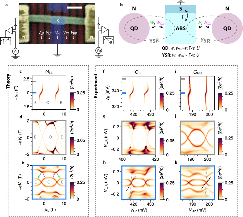
Fig. 1a shows a scanning electron microscope image of the reported device. It consists of an InSb nanowire (green) placed on top of a series of bottom gates Badawy.2019 . The middle part of the nanowire is covered by a thin Al shell (blue), forming a superconductor-semiconductor hybrid whose electrochemical potential is controlled by a plunger gate (). On both sides of the hybrid segment, QDs are formed in the nanowire using three gates each. The electrochemical potential of each QD is controlled by a plunger gate ( and for the left and right QDs, respectively), and the couplings between the QDs and the hybrid are controlled by tunnel gates ( and for the left and right QDs, respectively). A normal lead is attached to each QD, separated by another gate-defined tunnel barrier. The superconducting lead is kept grounded at all times. In addition, the two normal leads are connected to off-chip multiplexed resonators for fast RF reflectometry measurements Hornibrook.2014 , using the setup described in Ref. wang2022parametric . Each lead is voltage biased independently with respect to the grounded Al, with voltages and on the left and right leads, respectively. The currents ( and on the left and right leads), the local conductances (, ), and the non-local conductances (, ) are measured simultaneously. When the full conductance matrix is measured, we correct for line resistance as described in the Methods section. Further fabrication and setup details can be found in our previous publications Heedt.2021 ; Borsoi.2021 ; Mazur.2022 . The experiment is conducted in a dilution refrigerator with a base temperature of . A magnetic field of is applied along the nanowire axis, inducing a Zeeman splitting of approximately in the QDs (Fig. ED1).
2 YSR states in quantum dots
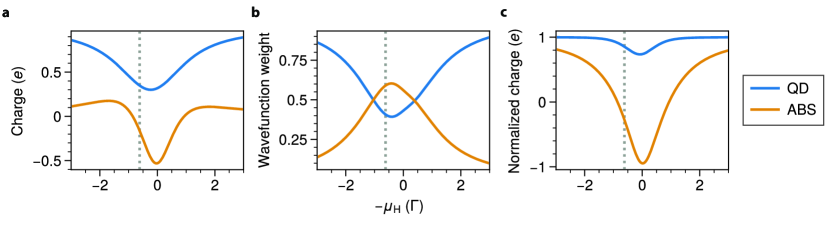
We model our system using a three-site model in which the hybrid is considered as a single Andreev bound state (ABS) in the atomic limit Bauer.2007 ; meng2009self tunnel-coupled to two QDs (see schematics in Fig. 1b) Tsintzis.2022 . The QDs have charging energy , Zeeman splitting , and chemical potentials for the left and right QD, respectively. The ABS has an induced gap , which in the atomic limit Bauer.2007 ; meng2009self can be identified with its tunnel coupling to the bulk superconductor. Its charging energy is negligible due to the screening of the grounded Al film. It also has Zeeman splitting , which is smaller than that of the QDs due to metallization of the ABS Reeg.2018 . We ensure so that the ground state of the ABS is always a BCS singlet. The electron-hole composition of the ABS depends on its chemical potential .
In our model, the QDs are coupled to the ABS by spin-conserving and spin-flipping tunneling due to spin-orbit interaction, with amplitudes and , respectively Tsintzis.2022 . The hybridization between QDs and the ABS becomes significant when . As a consequence, the QDs become proximitized and form YSR states Grove-Rasmussen.2018 ; Liu.2023 , which we distinguish from ABSs because of their large charging energy Bauer.2007 ; meng2009self ; GroveRasmussen.2009 ; Chang.2013 ; kirsanskas2015YuShibaRusinov ; Jellinggaard.2016 . We refer readers to the Supplementary Information and the parallel work of Ref. Liu.2023 for theory models of the strong coupling regime investigated in this work.
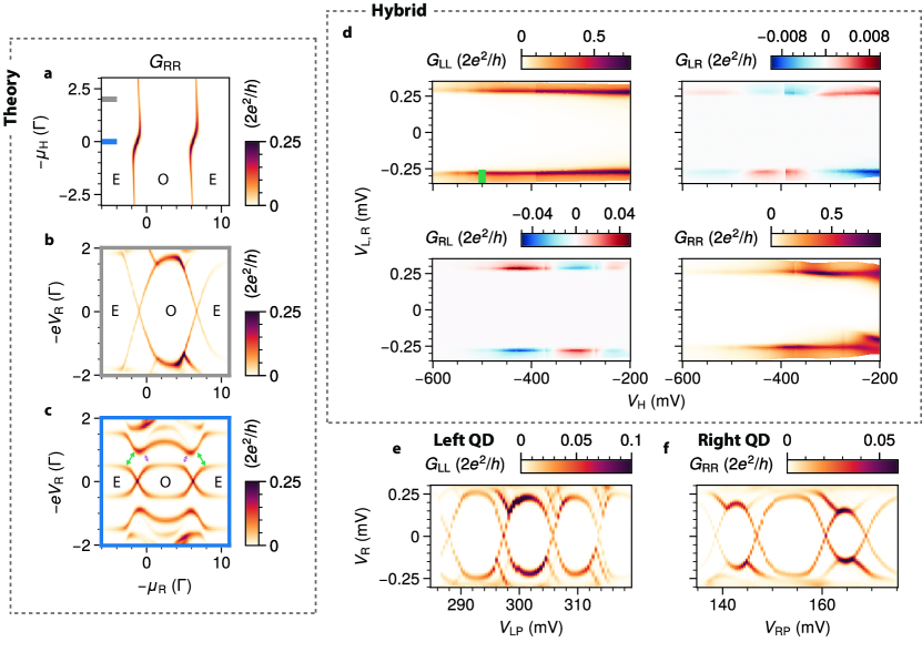
To understand the nature of the YSR states formed in proximitized QDs, we first examine the coupling between a single QD and an ABS in the hybrid segment, following Ref. Grove-Rasmussen.2018 . Fig. 1c shows the theoretical zero-bias conductance of a QD-ABS charge stability diagram (CSD), while the second QD is off-resonance. The two vertical features indicate parity transitions of the system, largely corresponding to the consecutive filling of a single orbital of the QD by two electrons. The S-shaped conductance features result from renormalization of the QD energy via hybridization with the ABS. The ABS reaches its energy minimum at charge neutrality, i.e., , where its excitation is equal-parts electron and hole. The hybridization with the QD is also maximal here due to their minimal energy separation, evident in the enhanced zero-bias conductance as local Andreev reflection becomes stronger Grove-Rasmussen.2018 ; Liu.2023 . The QD spectra in panels d and e further reveal its hybridization with the ABS. When the latter is away from charge neutrality, the QD spectrum as a function of (Fig. 1d) exhibits straight features reminiscent of Coulomb diamonds. As the ABS approaches (Fig. 1e), such features evolve into an eye-shaped spectrum typical of YSR states Pillet.2010 ; Lee.2014 ; Jellinggaard.2016 ; Scherbl2020 ; Scherbl2022 . The arrows indicate avoided crossings in the excited states of the spectrum produced by spin-conserving (green) and spin-flipping (pink) tunneling between the ABS and the QD levels Liu.2023 .
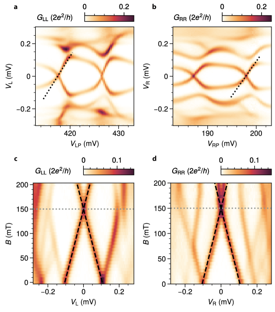
The hybrid segment of our device features multiple discrete ABSs well-separated from each other in (Fig. ED2). We operate in a range containing a single ABS level. In Fig. 1f, we show the zero-bias conductance measured with the left lead as a function of and . is fixed to keep the right QD off-resonance. We observe the QD-ABS charge stability diagram features described in panel c, indicating the presence of an ABS reaching its energy minimum at . The QD-ABS hybridization is further confirmed by the QD spectrum being in agreement with the model when the ABS is away from (Fig. 1g) and at its energy minimum (Fig. 1h).
The YSR zero-energy excitations in Fig. 1h are our building blocks of a Kitaev chain. Compared to a non-proximitized QD zero-energy crossing, these YSR crossings have noticeably weaker energy dispersion as a function of gate (see dashed lines in panel h). To quantify this observation, we can estimate the lever arm of the YSR excitation at charge degeneracy using its gate-dispersion slope: . In contrast to the above-gap QD lever arm of in our devices (Fig. ED3a), this subgap lever arm reduces to (Fig. ED3b) when the ABS is detuned from its charge neutrality. Tuning the ABS to its energy minimum further reduces the lever arm to (Fig. 1h). This signals a strong reduction in the effective charge of the fermionic excitation, attributable to charging energy renormalization, QD-ABS hybridization, and electron-hole superposition Schindele.2014 ; gramich2017Andreev , as detailed in Fig. ED4.
The right QD shows similar behavior when coupled to the same ABS (Fig. 1i–k). However, when the ABS is away from charge neutrality, the subgap conductance is not significantly suppressed (Fig. 1i) and the QD spectrum still shows typical YSR features (Fig. 1h), albeit with a small superconducting coupling. This could be due to residual proximity resulting from direct coupling between the QD and the superconducting film since does not affect it appreciably (Fig. ED5).
3 Coupled YSR states
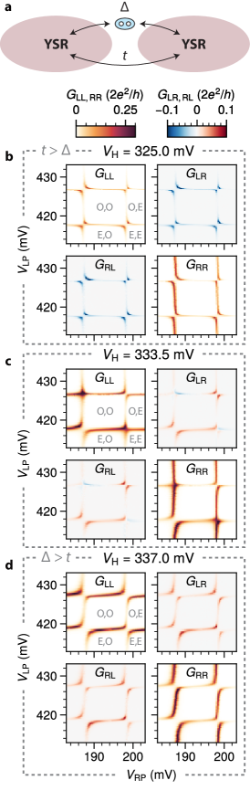
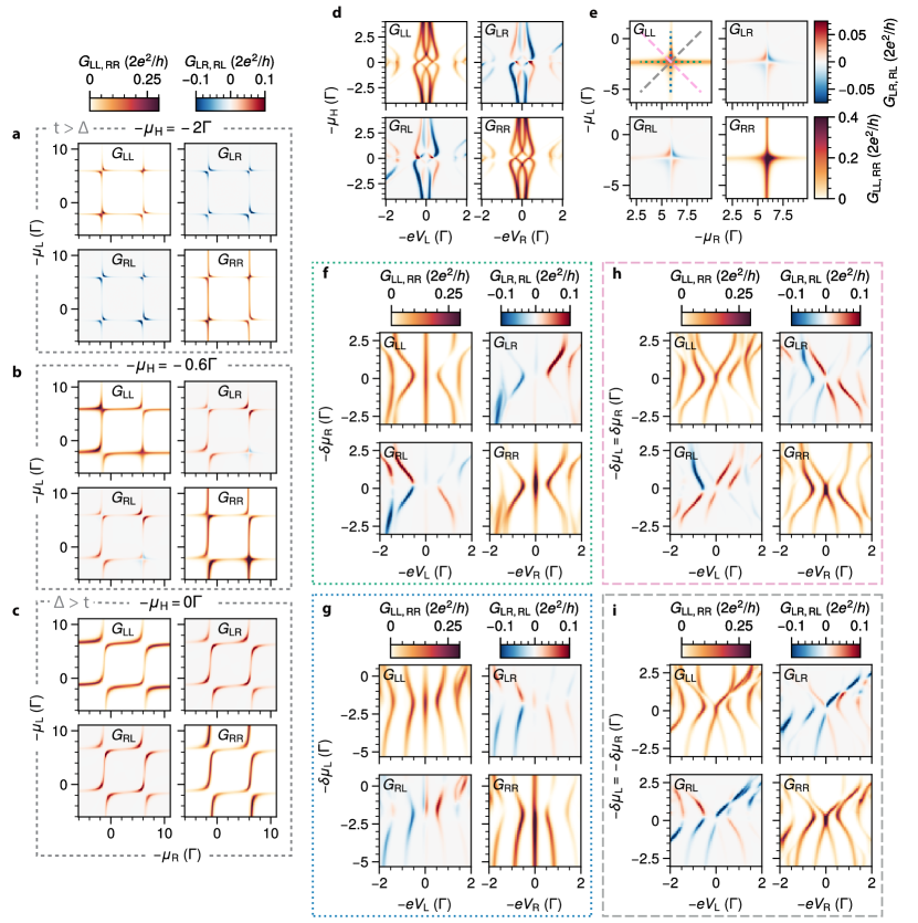
Recent theoretical Liu.2022 ; Tsintzis.2022 and experimental Wang.2022 ; Dvir.2023 ; Bordin.2022 works have shown that an ABS can mediate elastic co-tunneling (ECT) and crossed Andreev reflection (CAR) between QDs. These two processes implement the hopping and pairing terms of the original Kitaev chain model Kitaev.2001 ; Sau.2012 . To form PMM states in a two-site chain, the amplitudes of both terms must be equal Leijnse.2012 . Such control can be achieved by tuning the electrochemical potential of the ABS in the hybrid nanowire Liu.2022 ; Tsintzis.2022 ; Dvir.2023 ; Bordin.2022 .
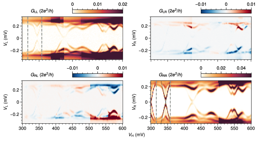
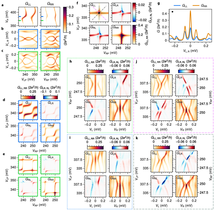
Similar effective ECT and CAR couplings, with respective amplitudes and , also emerge between YSR states (Fig. 2a) formed by strongly coupling QDs to the same ABS Trocha2015 ; Scherbl2019 ; Liu.2023 . To observe them, we turn to the CSD of two such YSR states, akin to those explored in Refs. EstradaSaldaa2020 ; Krtssy2021 . In Fig. 2b, we show the zero-bias conductance matrix measured as a function and when the ABS is tuned away from its energy minimum. All elements of the conductance matrix show prominent resonances arising from the two charge transitions of each QD. The type of avoided crossings observed in the CSD serves as an indication of the coupled-YSR system’s ground state Tsintzis.2022 ; Dvir.2023 . Avoided crossings along a negative diagonal, as seen in all four resonances in Fig. 2b, show hybridization between states with the same total charge. This is the ground state of the system when . This observation is further confirmed by the negative non-local conductance that is characteristic of ECT Dvir.2023 .
Increasing the value of leads to a change in the CSD, shown in Fig. 2c. Here, the bottom-left and the top-right resonances show avoided crossings along a positive diagonal associated with . In the top-left and bottom-right, the resonance lines cross each other, indicating a PMM sweet spot, with . Finally, bringing the ABS close to its energy minimum by a further increase of tunes all of the quadrants of the CSD to the regime (Fig. 2d). The theoretical model reproduces the observed evolution of the CSDs (Fig. ED6a–c).
4 Gate control of CAR and ECT
ABS-mediated ECT and CAR couplings between QDs are controlled by the chemical potential of ABS Liu.2022 ; Bordin.2022 . At the energy minimum of the ABS, its excitation is equally electron- and hole-like, both parts interfering constructively to enhance CAR and destructively to quench ECT. Finite values of lead to an imbalance between the electron and hole parts of the ABS, decreasing the value of the CAR coupling while enhancing ECT. This control over the ECT and CAR amplitudes guarantees a PMM sweet spot when the two QDs are coupled via a single ABS Liu.2022 ; Bordin.2022 ; Tsintzis.2022 . To demonstrate that this description can be extended to YSR states coupled via an ABS, we study how the couplings and vary as the electrochemical potential of the ABS changes.
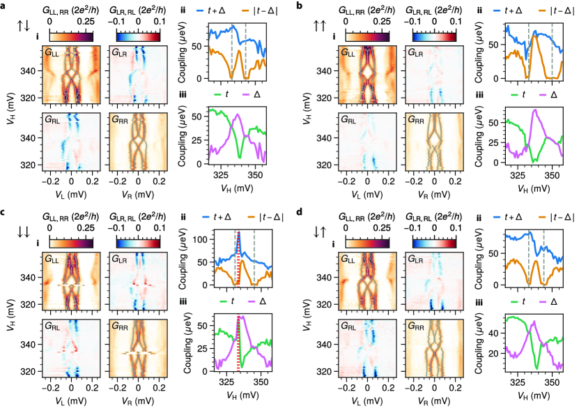
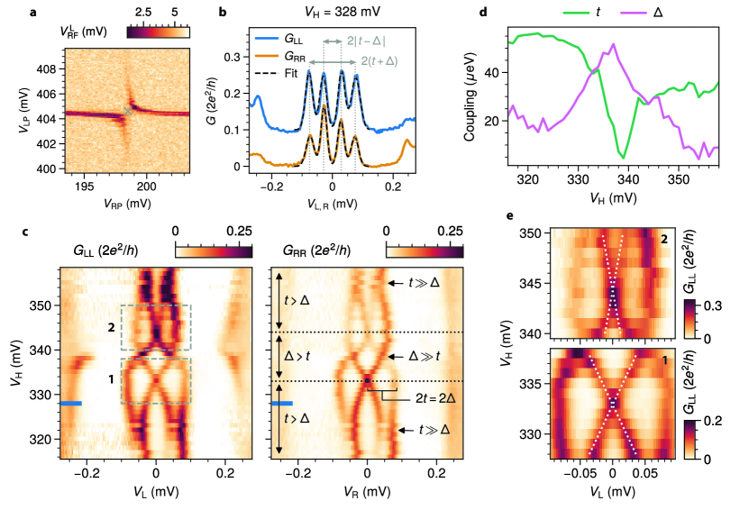
The magnitudes of and can be extracted by measuring the excitation spectrum of the system at , when spectral splitting is determined by the couplings alone. We limit the discussion here to the bottom-right crossing of Fig. 2, noting that the other crossings exhibit qualitatively similar behavior (Fig. ED7). At each fixed value of , we measure a CSD (Fig. 3a) and set the QD gates to the center of an avoided crossing. There, the subgap spectrum exhibits two sets of electron-hole symmetric peaks at energies and (Fig. 3b), as detailed in Methods. By fitting the measured spectrum with two pairs of Gaussians symmetric around , we extract the energy of the excited states and calculate and . We repeat this procedure for different values of and collect the spectra in Fig. 3c, where each line was measured as described above.
Fig. 3d shows the extracted values of ECT and CAR amplitudes. At and , the outer peaks almost merge with the inner ones, indicating . Inspecting the corresponding CSDs (see Fig. 2b for an example, all the CSDs are available in the online repository), we can see that ECT is dominant and, therefore, . Upon varying , the two peaks split into four well-separated peaks, signaling that CAR is increasing although ECT still prevails. At and , the two inner peaks merge into a single zero-bias peak. These are two sweet spots where . In between them, CAR dominates, as the CSDs can confirm (see Fig. 2d). Around , the outer peaks merge again, this time indicating . This feature is the peak in and dip in seen in Fig. 3d, because of the aforementioned interference effects Liu.2022 ; Bordin.2022 . Finally, Fig. ED6d shows that the same spectral features are reproduced by the theoretical model.
The zero-energy crossings in Fig. 3e allow us to characterize the robustness of the PMM sweet spots to charge fluctuations affecting the ABS and, consequently, and , causing a splitting of the zero-energy states. Indeed, we observe that each zero energy state splits with a linear dependence on as predicted by theory, indicating the lack of protection against deviations from the condition known for a two-site Kitaev chain Leijnse.2012 . We extract a slope of and for the two crossings, comparable to what we measured in Ref. Dvir.2023 .
5 Majorana sweet spot
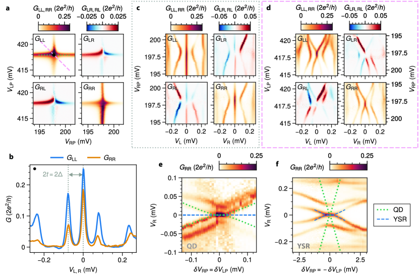
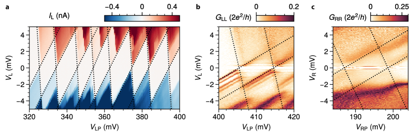
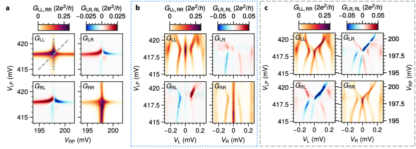
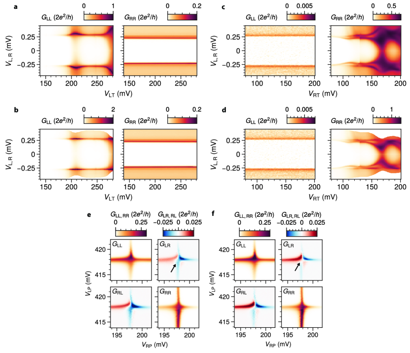
Finally, we measure the spectrum and stability of the PMM states against perturbation of the QDs. We tune our device to the sweet spot at , where . In Fig. 4a, we show the full conductance matrix of the CSD at the sweet spot. As expected, the resonance lines cross each other and non-local conductance alternates between positive and negative values. The spectrum measured at the sweet spot in the center of the CSD (Fig. 4b) shows, on both sides of the device, a zero-bias conductance peak clearly separated from the excited states. As a result of the much stronger coupling between YSR states, the first excited states reside at energies of , three times larger than in our previous report Dvir.2023 and significantly above the electron temperature.
One of the hallmarks of PMM states is their stability against local perturbations. In Fig. 4c, we measure the spectrum of the QDs varying while keeping the left QD on resonance. The observed zero-bias conductance peak persists within the range of the investigated charge degeneracy. Tuning while keeping the right QD on resonance (Fig. ED8b) shows the same qualitative features. The same behavior can be reproducibly observed with other QD and ABS orbitals, as shown in Fig. ED9.
If the electrochemical potentials of both QDs are detuned from the sweet spot, PMM states are expected to split quadratically. This is verified in Fig. 4d, where we measure the spectrum while detuning both QDs along the antidiagonal path shown in Fig. 4a. The spectrum taken along the diagonal path is shown in Fig. ED8c. Numerical simulations reproducing these measurements are reported in Fig. ED6e–i. For comparison, we plot the quadratic dispersion measurements of the QD-based vs YSR-based PMMs side by side in panels e and f. The curvature of the energy-gate dispersion close to the sweet spot is directly proportional to the dephasing rate resulting from charge noise affecting both QDs Aasen.2016 ; Knapp.2018 ; Mishmash.2020 ; Boross.2022 and is therefore a measure of the Majorana states’ robustness against it. Comparing the overlaid curves in Fig. 4e and f, we find the gate dispersion curvature reported in this work to be a factor of lower than the non-proximitized case (details in Materials and Methods). This striking reduction can be fully explained by the decreased lever arm of the YSR states, and the increased , since the curvature expected from the theory model is (see Materials and Methods).
To illustrate the effect of reduced charge dispersion on the coherence of a potential poor man’s Majorana qubit, we calculate the dephasing rates using realistic charge noise estimations and data presented above (see Supplementary Information). While perturbation of QDs’ potentials is expected to be the dominant mechanism of energy splitting and thus dephasing for non-proximitized PMMs, the drastic reduction in gate dispersion of YSR-based PMMs makes it negligible compared to dephasing caused by deviations from the condition. The estimated is now limited by noise affecting the couplings and , nearly an order of magnitude higher than the charge-noise-limited extracted from data in our previous report Dvir.2023 . Importantly, the expected dephasing time is now also much longer than the adiabatic limit , which sets an upper bound on how fast Majorana states can be manipulated without populating the excited states Aasen.2016 ; Boross.2023 .
6 Conclusion
In conclusion, we have demonstrated the formation of YSR states by hybridizing QDs with a common ABS. The coupling between these YSR states can be controlled by varying the electrochemical potential of the ABS, thus realizing a fully tunable two-site Kitaev chain. The resulting PMM states have two significant improvements over those in a non-proximitized QD chain. First, the stronger coupling between the YSR states triples the gap between the PMM and excited states, protecting the former from finite temperature excitations Knapp.2018 and enabling faster adiabatic operations Aasen.2016 ; Boross.2023 . Second, the reduced charge dispersion of the YSR states enhances the robustness of the PMMs against charge noise affecting both QDs by more than 100. Thanks to these, even a two-site Kitaev chain realized using YSR states should suffice for a prototypical Majorana qubit and verification of non-abelian properties with fusion and braiding experiments. Despite the present lack of protection against tunnel-coupling noise, the expected coherence of Majorana qubits made from PMM states is increased by close to an order of magnitude compared to the first report Dvir.2023 . In the future, increasing the number of sites can mitigate noise affecting the tunnel-coupling rates. Estimations using parameters of the YSR-based PMMs suggest that a Majorana qubit realized with Kitaev chains as short as 3 to 5 sites could already achieve dephasing times comparable to those predicted for continuous nanowires Sau.2012 ; Knapp.2018 .
7 Data availability and code availability
Raw data presented in this work, the data processing/plotting code, and code used for the theory calculations are available at https://zenodo.org/records/10013728.
8 Acknowledgements
This work has been supported by the Dutch Organization for Scientific Research (NWO) and Microsoft Corporation Station Q. We thank John M. Hornibrook and David J. Reilly for providing the frequency multiplexing chips. We thank Martin Leijnse, Ville Maisi, Pasquale Scarlino, Athanasios Tsintzis, Rubén Seoane Souto, Karsten Flensberg, Srijit Goswami, Sebastiaan L. D. ten Haaf, Qingzhen Wang, Ivan Kulesh, and Yining Zhang for helpful discussions.
9 Author contributions
DvD, FZ, AB, GPM, NvL, and JCW fabricated the device. FZ, DvD, DX, BR, and TD performed the electrical measurements. TD and GW designed the experiment. FZ, DvD, GW, and TD analyzed the data. FZ, DvD, TD, GW, and LPK prepared the manuscript with input from all authors. TD and LPK supervised the project. CXL and AMB developed the theoretical model with input from MW. G.B., S.G., and E.P.A.M.B. performed InSb nanowire growth.
10 Competing interests
The authors declare no competing interests.
References
- \bibcommenthead
- (1) Kitaev, A.Y.: Unpaired Majorana fermions in quantum wires. Physics-Uspekhi 44(10S), 131 (2001). https://doi.org/10.1070/1063-7869/44/10s/s29
- (2) Sau, J.D., Sarma, S.D.: Realizing a robust practical Majorana chain in a quantum-dot-superconductor linear array. Nature Communications 3(1), 964 (2012). https://doi.org/10.1038/ncomms1966
- (3) Leijnse, M., Flensberg, K.: Parity qubits and poor man’s Majorana bound states in double quantum dots. Physical Review B 86(13), 134528 (2012). https://doi.org/10.1103/PhysRevB.86.134528
- (4) Liu, C.-X., Pan, H., Setiawan, F., Wimmer, M., Sau, J.D.: Fusion protocol for Majorana modes in coupled quantum dots. Physical Review B 108(8), 085437 (2023). https://doi.org/%****␣article_new_14062023.bbl␣Line␣100␣****10.1103/PhysRevB.108.085437
- (5) Boross, P., Pályi, A.: Braiding-based quantum control of a Majorana qubit built from quantum dots. arXiv (2023). https://doi.org/10.48550/arXiv.2305.08464
- (6) Tsintzis, A., Souto, R.S., Flensberg, K., Danon, J., Leijnse, M.: Roadmap towards Majorana qubits and nonabelian physics in quantum dot-based minimal Kitaev chains. arXiv (2023). https://doi.org/10.48550/arXiv.2306.16289
- (7) Pino, D.M., Souto, R.S., Aguado, R.: Minimal Kitaev-transmon qubit based on double quantum dots. arXiv (2023). https://doi.org/10.48550/arXiv.2309.12313
- (8) Dvir, T., Wang, G., van Loo, N., Liu, C.-X., Mazur, G.P., Bordin, A., ten Haaf, S.L.D., Wang, J.-Y., van Driel, D., Zatelli, F., Li, X., Malinowski, F.K., Gazibegovic, S., Badawy, G., Bakkers, E.P.A.M., Wimmer, M., Kouwenhoven, L.P.: Realization of a minimal Kitaev chain in coupled quantum dots. Nature 614(7948), 445–450 (2023). https://doi.org/10.1038/s41586-022-05585-1
- (9) Koch, J., Yu, T.M., Gambetta, J., Houck, A.A., Schuster, D.I., Majer, J., Blais, A., Devoret, M.H., Girvin, S.M., Schoelkopf, R.J.: Charge-insensitive qubit design derived from the Cooper pair box. Physical Review A 76(4), 042319 (2007). https://doi.org/10.1103/PhysRevA.76.042319
- (10) Schreier, J.A., Houck, A.A., Koch, J., Schuster, D.I., Johnson, B.R., Chow, J.M., Gambetta, J.M., Majer, J., Frunzio, L., Devoret, M.H., Girvin, S.M., Schoelkopf, R.J.: Suppressing charge noise decoherence in superconducting charge qubits. Physical Review B 77(18), 180502 (2008). https://doi.org/10.1103/PhysRevB.77.180502
- (11) Yu, L.: Bound state in superconductors with paramagnetic impurities. Acta Phys. Sin. 21, 75–91 (1965)
- (12) Shiba, H.: Classical Spins in Superconductors. Progress of Theoretical Physics 40(3), 435–451 (1968). https://doi.org/10.1143/PTP.40.435
- (13) Rusinov, A.: Superconductivity near a paramagnetic impurity. JETP Lett. 9 (1969)
- (14) Buitelaar, M.R., Nussbaumer, T., Schönenberger, C.: Quantum dot in the Kondo regime coupled to superconductors. Physical Review Letters 89(25), 256801 (2002). https://doi.org/10.1103/PhysRevLett.89.256801
- (15) Bauer, J., Oguri, A., Hewson, A.C.: Spectral properties of locally correlated electrons in a Bardeen–Cooper–Schrieffer superconductor. Journal of Physics: Condensed Matter 19(48), 486211 (2007). https://doi.org/10.1088/0953-8984/19/48/486211
- (16) Meng, T., Florens, S., Simon, P.: Self-consistent description of Andreev bound states in Josephson quantum dot devices. Physical Review B 79(22), 224521 (2009). https://doi.org/10.1103/PhysRevB.79.224521
- (17) Grove-Rasmussen, K., Jørgensen, H.I., Andersen, B.M., Paaske, J., Jespersen, T.S., Nygård, J., Flensberg, K., Lindelof, P.E.: Superconductivity-enhanced bias spectroscopy in carbon nanotube quantum dots. Physical Review B 79(13), 134518 (2009). https://doi.org/10.1103/PhysRevB.79.134518
- (18) Chang, W., Manucharyan, V.E., Jespersen, T.S., Nygård, J., Marcus, C.M.: Tunneling spectroscopy of quasiparticle bound states in a spinful Josephson junction. Physical Review Letters 110(21), 217005 (2013). https://doi.org/10.1103/PhysRevLett.110.217005
- (19) Jellinggaard, A., Grove-Rasmussen, K., Madsen, M.H., Nygård, J.: Tuning Yu-Shiba-Rusinov states in a quantum dot. Physical Review B 94(6), 064520 (2016). https://doi.org/10.1103/PhysRevB.94.064520
- (20) Grove-Rasmussen, K., Steffensen, G., Jellinggaard, A., Madsen, M.H., Žitko, R., Paaske, J., Nygård, J.: Yu–Shiba–Rusinov screening of spins in double quantum dots. Nature Communications 9(1), 2376 (2018). https://doi.org/10.1038/s41467-018-04683-x
- (21) Fulga, I.C., Haim, A., Akhmerov, A.R., Oreg, Y.: Adaptive tuning of Majorana fermions in a quantum dot chain. New Journal of Physics 15(4), 045020 (2013). https://doi.org/10.1088/1367-2630/15/4/045020
- (22) Nadj-Perge, S., Drozdov, I.K., Bernevig, B.A., Yazdani, A.: Proposal for realizing Majorana fermions in chains of magnetic atoms on a superconductor. Physical Review B 88(2), 020407 (2013). https://doi.org/%****␣article_new_14062023.bbl␣Line␣400␣****10.1103/PhysRevB.88.020407
- (23) Pientka, F., Peng, Y., Glazman, L., von Oppen, F.: Topological superconducting phase and Majorana bound states in Shiba chains. Physica Scripta 2015(T164), 014008 (2015). https://doi.org/10.1088/0031-8949/2015/T164/014008
- (24) Schecter, M., Flensberg, K., Christensen, M.H., Andersen, B.M., Paaske, J.: Self-organized topological superconductivity in a Yu-Shiba-Rusinov chain. Physical Review B 93(14), 140503 (2016). https://doi.org/10.1103/PhysRevB.93.140503
- (25) Liu, C.-X., Wang, G., Dvir, T., Wimmer, M.: Tunable superconducting coupling of quantum dots via Andreev bound states in semiconductor-superconductor nanowires. Physical Review Letters 129(26), 267701 (2022). https://doi.org/10.1103/PhysRevLett.129.267701
- (26) Tsintzis, A., Souto, R.S., Leijnse, M.: Creating and detecting poor man’s Majorana bound states in interacting quantum dots. Physical Review B 106(20), 201404 (2022). https://doi.org/10.1103/PhysRevB.106.l201404
- (27) Nadj-Perge, S., Drozdov, I.K., Li, J., Chen, H., Jeon, S., Seo, J., MacDonald, A.H., Bernevig, B.A., Yazdani, A.: Observation of Majorana fermions in ferromagnetic atomic chains on a superconductor. Science 346(6209), 602–607 (2014). https://doi.org/10.1126/science.1259327
- (28) Ruby, M., Pientka, F., Peng, Y., von Oppen, F., Heinrich, B.W., Franke, K.J.: End states and subgap structure in proximity-coupled chains of magnetic adatoms. Physical Review Letters 115(19), 197204 (2015). https://doi.org/10.1103/PhysRevLett.115.197204
- (29) Jeon, S., Xie, Y., Li, J., Wang, Z., Bernevig, B.A., Yazdani, A.: Distinguishing a Majorana zero mode using spin-resolved measurements. Science 358(6364), 772–776 (2017). https://doi.org/10.1126/science.aan3670
- (30) Schneider, L., Beck, P., Posske, T., Crawford, D., Mascot, E., Rachel, S., Wiesendanger, R., Wiebe, J.: Topological Shiba bands in artificial spin chains on superconductors. Nature Physics 17(8), 943–948 (2021). https://doi.org/10.1038/s41567-021-01234-y
- (31) Schneider, L., Beck, P., Neuhaus-Steinmetz, J., Rózsa, L., Posske, T., Wiebe, J., Wiesendanger, R.: Precursors of Majorana modes and their length-dependent energy oscillations probed at both ends of atomic Shiba chains. Nature Nanotechnology 17(4), 384–389 (2022). https://doi.org/10.1038/s41565-022-01078-4
- (32) ten Haaf, S.L.D., Wang, Q., Bozkurt, A.M., Liu, C.-X., Kulesh, I., Kim, P., Xiao, D., Thomas, C., Manfra, M.J., Dvir, T., Wimmer, M., Goswami, S.: Realizing Majorana bound states through interacting quantum dots in a two-dimensional electron gas. arXiv (2023)
- (33) Badawy, G., Gazibegovic, S., Borsoi, F., Heedt, S., Wang, C.-A., Koelling, S., Verheijen, M.A., Kouwenhoven, L.P., Bakkers, E.P.A.M.: High Mobility Stemless InSb Nanowires. Nano Letters 19(6), 3575–3582 (2019). https://doi.org/10.1021/acs.nanolett.9b00545
- (34) Hornibrook, J.M., Colless, J.I., Mahoney, A.C., Croot, X.G., Blanvillain, S., Lu, H., Gossard, A.C., Reilly, D.J.: Frequency multiplexing for readout of spin qubits. Applied Physics Letters 104(10), 103108 (2014). https://doi.org/10.1063/1.4868107
- (35) Wang, J.-Y., van Loo, N., Mazur, G.P., Levajac, V., Malinowski, F.K., Lemang, M., Borsoi, F., Badawy, G., Gazibegovic, S., Bakkers, E.P.A.M., Quintero-Pérez, M., Heedt, S., Kouwenhoven, L.P.: Parametric exploration of zero-energy modes in three-terminal InSb-Al nanowire devices. Physical Review B 106(7), 075306 (2022). https://doi.org/10.1103/PhysRevB.106.075306
- (36) Heedt, S., Quintero-Pérez, M., Borsoi, F., Fursina, A., Loo, N.v., Mazur, G.P., Nowak, M.P., Ammerlaan, M., Li, K., Korneychuk, S., Shen, J., Poll, M.A.Y.v.d., Badawy, G., Gazibegovic, S., Jong, N.d., Aseev, P., Hoogdalem, K.v., Bakkers, E.P.A.M., Kouwenhoven, L.P.: Shadow-wall lithography of ballistic superconductor–semiconductor quantum devices. Nature Communications 12(1), 4914 (2021). https://doi.org/10.1038/s41467-021-25100-w
- (37) Borsoi, F., Mazur, G.P., van Loo, N., Nowak, M.P., Bourdet, L., Li, K., Korneychuk, S., Fursina, A., Wang, J., Levajac, V., Memisevic, E., Badawy, G., Gazibegovic, S., Hoogdalem, K.v., Bakkers, E.P.A.M., Kouwenhoven, L.P., Heedt, S., Quintero‐Pérez, M.: Single‐shot fabrication of semiconducting–superconducting nanowire devices. Advanced Functional Materials 31(34), 2102388 (2021). https://doi.org/10.1002/adfm.202102388
- (38) Mazur, G.P., van Loo, N., Wang, J.-Y., Dvir, T., Wang, G., Khindanov, A., Korneychuk, S., Borsoi, F., Dekker, R.C., Badawy, G., Vinke, P., Gazibegovic, S., Bakkers, E.P.A.M., Pérez, M.Q.-, Heedt, S., Kouwenhoven, L.P.: Spin-Mixing Enhanced Proximity Effect in Aluminum-Based Superconductor–Semiconductor Hybrids. Advanced Materials 34(33), 2202034 (2022). https://doi.org/10.1002/adma.202202034
- (39) Reeg, C., Loss, D., Klinovaja, J.: Metallization of a Rashba wire by a superconducting layer in the strong-proximity regime. Physical Review B 97(16), 165425 (2018). https://doi.org/10.1103/PhysRevB.97.165425
- (40) Liu, C.-X., Bozkurt, A.M., Zatelli, F., ten Haaf, S.L.D., Dvir, T., Wimmer, M.: Enhancing the excitation gap of a quantum-dot-based Kitaev chain. arXiv (2023). https://doi.org/10.48550/arXiv.2310.09106
- (41) Kiršanskas, G., Goldstein, M., Flensberg, K., Glazman, L.I., Paaske, J.: Yu-Shiba-Rusinov states in phase-biased superconductor–quantum dot–superconductor junctions. Physical Review B 92(23), 235422 (2015). https://doi.org/10.1103/PhysRevB.92.235422
- (42) Pillet, J.-D., Quay, C.H.L., Morfin, P., Bena, C., Yeyati, A.L., Joyez, P.: Andreev bound states in supercurrent-carrying carbon nanotubes revealed. Nature Physics 6(12), 965–969 (2010). https://doi.org/10.1038/nphys1811
- (43) Lee, E.J.H., Jiang, X., Houzet, M., Aguado, R., Lieber, C.M., Franceschi, S.D.: Spin-resolved Andreev levels and parity crossings in hybrid superconductor–semiconductor nanostructures. Nature Nanotechnology 9(1), 79–84 (2014). https://doi.org/10.1038/nnano.2013.267
- (44) Scherübl, Z., Fülöp, G., Moca, C.P., Gramich, J., Baumgartner, A., Makk, P., Elalaily, T., Schönenberger, C., Nygård, J., Zaránd, G., Csonka, S.: Large spatial extension of the zero-energy Yu-Shiba-Rusinov state in a magnetic field. Nature Communications 11(1) (2020). https://doi.org/10.1038/s41467-020-15322-9
- (45) Scherübl, Z., Fülöp, G., Gramich, J., Pályi, A., Schönenberger, C., Nygård, J., Csonka, S.: From cooper pair splitting to nonlocal spectroscopy of a Shiba state. Physical Review Research 4(2) (2022). https://doi.org/10.1103/PhysRevResearch.4.023143
- (46) Schindele, J., Baumgartner, A., Maurand, R., Weiss, M., Schönenberger, C.: Nonlocal spectroscopy of Andreev bound states. Physical Review B 89(4), 045422 (2014). https://doi.org/10.1103/PhysRevB.89.045422
- (47) Gramich, J., Baumgartner, A., Schönenberger, C.: Andreev bound states probed in three-terminal quantum dots. Physical Review B 96(19), 1–14 (2017). https://doi.org/10.1103/PhysRevB.96.195418
- (48) Wang, G., Dvir, T., Mazur, G.P., Liu, C.-X., van Loo, N., ten Haaf, S.L.D., Bordin, A., Gazibegovic, S., Badawy, G., Bakkers, E.P.A.M., Wimmer, M., Kouwenhoven, L.P.: Singlet and triplet Cooper pair splitting in hybrid superconducting nanowires. Nature 612(7940), 448–453 (2022). https://doi.org/10.1038/s41586-022-05352-2
- (49) Bordin, A., Wang, G., Liu, C.-X., ten Haaf, S.L.D., van Loo, N., Mazur, G.P., Xu, D., van Driel, D., Zatelli, F., Gazibegovic, S., Badawy, G., Bakkers, E.P.A.M., Wimmer, M., Kouwenhoven, L.P., Dvir, T.: Tunable crossed Andreev reflection and elastic cotunneling in hybrid nanowires. Physical Review X 13(3), 031031 (2023). https://doi.org/10.1103/PhysRevX.13.031031
- (50) Trocha, P., Weymann, I.: Spin-resolved Andreev transport through double-quantum-dot cooper pair splitters. Physical Review B 91(23) (2015). https://doi.org/10.1103/PhysRevB.91.235424
- (51) Scherübl, Z., Pályi, A., Csonka, S.: Transport signatures of an Andreev molecule in a quantum dot–superconductor–quantum dot setup. Beilstein Journal of Nanotechnology 10, 363–378 (2019). https://doi.org/10.3762/bjnano.10.36
- (52) Saldaña, J.C.E., Vekris, A., Žitko, R., Steffensen, G., Krogstrup, P., Paaske, J., Grove-Rasmussen, K., Nygård, J.: Two-impurity Yu-Shiba-Rusinov states in coupled quantum dots. Physical Review B 102(19) (2020). https://doi.org/10.1103/PhysRevB.102.195143
- (53) Kürtössy, O., Scherübl, Z., Fülöp, G., Lukács, I.E., Kanne, T., Nygård, J., Makk, P., Csonka, S.: Andreev molecule in parallel InAs nanowires. Nano Letters 21(19), 7929–7937 (2021). https://doi.org/10.1021/acs.nanolett.1c01956
- (54) Aasen, D., Hell, M., Mishmash, R.V., Higginbotham, A., Danon, J., Leijnse, M., Jespersen, T.S., Folk, J.A., Marcus, C.M., Flensberg, K., Alicea, J.: Milestones toward Majorana-based quantum computing. Physical Review X 6(3), 031016 (2016). https://doi.org/10.1103/PhysRevX.6.031016
- (55) Knapp, C., Karzig, T., Lutchyn, R.M., Nayak, C.: Dephasing of Majorana-based qubits. Physical Review B 97(12), 125404 (2018). https://doi.org/10.1103/PhysRevB.97.125404
- (56) Mishmash, R.V., Bauer, B., von Oppen, F., Alicea, J.: Dephasing and leakage dynamics of noisy Majorana-based qubits: Topological versus Andreev. Physical Review B 101(7), 075404 (2020). https://doi.org/10.1103/PhysRevB.101.075404
- (57) Boross, P., Pályi, A.: Dephasing of Majorana qubits due to quasistatic disorder. Physical Review B 105(3), 035413 (2022). https://doi.org/10.1103/PhysRevB.105.035413
- (58) Martinez, E.A., Pöschl, A., Hansen, E.B., van de Poll, M.A.Y., Vaitiekėnas, S., Higginbotham, A.P., Casparis, L.: Measurement circuit effects in three-terminal electrical transport measurements (2021). https://doi.org/10.48550/arXiv.2104.02671
- (59) Petersson, K.D., Petta, J.R., Lu, H., Gossard, A.C.: Quantum coherence in a one-electron semiconductor charge qubit. Physical Review Letters 105(24), 246804 (2010). https://doi.org/10.1103/PhysRevLett.105.246804
- (60) Dial, O.E., Shulman, M.D., Harvey, S.P., Bluhm, H., Umansky, V., Yacoby, A.: Charge noise spectroscopy using coherent exchange oscillations in a singlet-triplet qubit. Physical Review Letters 110(14), 146804 (2013). https://doi.org/10.1103/PhysRevLett.110.146804
- (61) Scarlino, P., Ungerer, J.H., van Woerkom, D.J., Mancini, M., Stano, P., Müller, C., Landig, A.J., Koski, J.V., Reichl, C., Wegscheider, W., Ihn, T., Ensslin, K., Wallraff, A.: In situ tuning of the electric-dipole strength of a double-dot charge qubit: Charge-noise protection and ultrastrong coupling. Physical Review X 12(3), 031004 (2022). https://doi.org/10.1103/PhysRevX.12.031004
- (62) Connors, E.J., Nelson, J.J., Edge, L.F., Nichol, J.M.: Charge-noise spectroscopy of Si/SiGe quantum dots via dynamically-decoupled exchange oscillations. Nature Communications 13(1), 940 (2022). https://doi.org/10.1038/s41467-022-28519-x
- (63) Burkard, G., Ladd, T.D., Pan, A., Nichol, J.M., Petta, J.R.: Semiconductor spin qubits. Reviews of Modern Physics 95(2), 025003 (2023). https://doi.org/10.1103/RevModPhys.95.025003
- (64) Rainis, D., Loss, D.: Majorana qubit decoherence by quasiparticle poisoning. Physical Review B 85(17), 174533 (2012). https://doi.org/10.1103/PhysRevB.85.174533
- (65) Hofmann, A., Karlewski, C., Heimes, A., Reichl, C., Wegscheider, W., Schön, G., Ensslin, K., Ihn, T., Maisi, V.F.: Phonon spectral density in a GaAs/AlGaAs double quantum dot. Physical Review Research 2(3), 033230 (2020). https://doi.org/10.1103/PhysRevResearch.2.033230
- (66) Ranni, A., Haldar, S., Havir, H., Lehmann, S., Scarlino, P., Baumgartner, A., Schönenberger, C., Thelander, C., Dick, K.A., Potts, P.P., Maisi, V.F.: Dephasing in a crystal-phase defined double quantum dot charge qubit strongly coupled to a high-impedance resonator. arXiv (2023). https://doi.org/10.48550/arXiv.2308.14887
11 Materials and Methods
11.1 Device fabrication
The InSb/Al hybrid nanowire device presented in this work was fabricated using the shadow-wall lithography technique Heedt.2021 ; Borsoi.2021 .
A substrate is patterned with Ti/Pd gates. of AlOx and of HfOx are deposited by ALD as gate dielectric. HSQ shadow-walls are then patterned. Nanowires are deposited and pushed next to the shadow-walls using an optical micro-manipulator. An Al shell is deposited at alternating angles of and with respect to the substrate, followed by a capping layer of of AlOx. Normal leads in ohmic contact with the nanowire are fabricated by Ar milling and evaporation of Cr/Au.
Additional details about the substrate fabrication and the Al deposition are described in Ref. Mazur.2022 .
11.2 Transport measurements and data processing
The measurements are done in a dilution refrigerator with a base temperature of . A magnetic field of is applied along the nanowire axis except in Fig. ED1c,d.
The three-terminal setup used to measure the device is illustrated in Fig. 1a. The SC lead is always kept grounded. The two normal leads can be voltage-biased independently. When a bias is applied to one side, the other one is kept grounded. The currents and are measured separately. Digital multimeters and lock-in amplifiers are used to read the voltage outputs of the current meters. AC excitations of RMS are applied on each side with different frequencies ( on the left and on the right), except for Fig. ED2 and Fig. ED5d–f, where excitations of RMS were used.
Off-chip multiplexed resonators Hornibrook.2014 connected to the two normal leads are used for fast RF reflectometry measurements. This measurement scheme was employed to speed up the tune-up of the device, for Fig. 3, and for Fig. ED7, as explained in Fig. 3a. Additional details about the reflectometry setup are described in Ref. wang2022parametric .
11.3 Spinless PMM spectrum
The low-energy spectrum of the coupled YSR system arising from the model described in Supplementary Information can be reduced to that of a spinless PMM model Leijnse.2012 ; Liu.2022 ; Tsintzis.2022 ; Liu.2023 ; Tsintzis.2023 .
In this simplified model, the non negative energy eigenvalues are Leijnse.2012
where , and are the chemical potentials of the two sites, and , are the couplings. The spectrum is symmetric around zero energy because of particle-hole symmetry. If , the eigenvalues reduce to and . These are the excitation energies that we use to extract and from the measured spectra in Fig. 3.
The gate dispersion lines plotted in Fig. 4e,f are calculated using the lowest excitation energy. When we obtain
where is the lever arm converting voltage to chemical potential and is the simultaneous detuning of each gate away from the sweet spot. For the PMM realized with QDs, we have used and Dvir.2023 . For the PMM realized with YSR states we have used (Fig. ED1) and (Fig. 4b). Finally, the quadratic splitting of PMM states can be derived by expanding the expression above for small , which gives
11.4 Series resistance correction
The effect of series resistance in the fridge line and other parts of the circuit on transport measurements of a three-terminal device of our type is described in Ref. Martinez2021 , as well as how to correct for it. In our setup, the resistance of the voltage source is and that of the current meter is . Additional series resistance comes from the fridge lines and the ohmic contacts. Correcting for the voltage fall over these resistors in series to the device requires knowledge of the exact resistance values, which we presently cannot obtain before the next sample exchange. Therefore, we make use of the fact that the bulk Al superconducting gap in local conductance measurements should stay constant across all gate values to arrive at an estimation of the total series resistance in each fridge line.
In Fig. ED10a,c it is possible to observe that the superconducting gap appears enlarged when there is finite subgap conductance, indicating unaccounted-for series resistance. To estimate it, we correct the measurement shown in Fig. ED10a for different trial values of the series resistance. We extract the energies of the coherence peaks and calculate their variance. Finally, we choose the value that minimizes the variance as the optimal series resistance. We find an optimal value of , in addition to the resistance of the voltage source and current meter. The corrected measurement is shown in Fig. ED10b. All the data processing steps are available in the online repository. In Fig. ED10c,d we show that the same series resistance value also corrects an analogous measurement on the right side. In the regimes relevant to this work, the voltage divider effect caused by the series resistance does not strongly affect local conductance. On the other hand, it can be more pronounced for non-local conductance, as discussed in Fig. ED10e,f. Using the extracted resistance value, we apply the correction method described in Ref. Martinez2021 to the data presented in Fig. 2, Fig. 3, Fig. 4, Fig. ED2, Fig. ED5d, Fig. ED7, Fig. ED8, Fig. ED9d–k, and Fig. ED10b,d,f, where the full conductance matrix is measured.
11.5 Device tune-up
The device is controlled with seven bottom gates (Fig. 1a). To perform tunnel spectroscopy of the hybrid segment in Fig. ED2 and Fig. ED5, we use and to form a tunnel barrier and apply a large positive voltage to , , and the outer gates. is used to control the electrochemical potential in the hybrid segment, where discrete states are confined because of the tunnel barriers. QDs are formed by reducing the voltage on the outer gates. This creates additional tunnel barriers next to the normal leads, thus shaping a confining potential. and control the electrochemical potential of the QDs. Finally, the coupling between the QDs and the ABS can be controlled using and . By increasing their voltage, we can achieve the strong coupling regime between the QDs and the ABS in the hybrid as explained in Fig. 1. For all the measurements presented in the main text, the gates defining the tunnel barriers were maintained at the same value.
12 Supplementary Information
12.1 Theoretical model
The physical system of double QDs connected by a hybrid segment in the middle can be well described by a three-site model as below
| (1) |
Here is the Hamiltonian for the QDs () or the ABS () in the hybrid, is the occupancy number of the QD orbital or normal state in the hybrid with spin , is the chemical potential energy, is the induced Zeeman energy, is the charging energy, and is the induced superconducting gap. is the tunnel Hamiltonian between the QDs and the ABS, where and are the amplitudes for the spin-conserving and spin-flipping single electron tunneling processes. The parameters used for the numerical simulations performed in this work, in unit of , the induced gap on the ABS, are: , for Zeeman energy, , for charging energy, , , , for tunneling amplitudes, and for induced gaps on the QDs. Here the magnitude of the Zeeman energy on the ABS is weaker than that in the QDs owing to the factor renormalization in the hybrid. Furthermore, an extra pairing gap is added on the right QD to explain the residual Andreev conductance when the ABS is far from its energy minimum, as shown in the measurement in Fig. 1. The sweet spot investigated in Fig. ED6e–i corresponds to , , and . Finally, in Fig. ED4, we calculate the electron and hole character of an excitation between two states of different parity as
| (2) |
where is the even state and the odd one.
In the experimental device, conductance spectroscopy of the hybrid system is measured in a three-terminal junction with two normal leads and one grounded superconducting lead. To numerically simulate the transport measurement, we attach two additional normal leads to the two QDs, respectively. The lead Hamiltonians are
| (3) |
where is the annihilation operator of a free electron with momentum and spin in lead-, is the kinetic energy, and is the lead chemical potential. The tunnel Hamiltonian between leads and the QDs is
| (4) |
where is the tunneling amplitude between QD- and lead-, and is assumed to be spin-diagonal and independent of . A more useful physical quantity to characterize the lead coupling strength is with being the density of states at the Fermi energy of the normal lead. Based on the model Hamiltonians introduced above, current and conductance matrices can be numerically calculated by solving a rate equation for the reduced density matrix of the hybrid system. We set the temperature and tunneling strength to be the same for both normal leads. Finally, when simulating the local Andreev conductance of a QD-ABS system, we are actually considering a two-terminal junction by removing the quantum dot and the normal lead on the other side.
12.2 Estimation of dephasing rates
A minimal Majorana qubit consists of two subsystems, each hosting one pair of Majoranas: , and . It is possible to encode a qubit in the subspace of either even or odd global fermion parity. Without loss of generality, we focus on the even subspace. We define qubit states , with the fermion parity of each subsystem being odd, and , each being even. The qubit Pauli operator is then identified as and the effective Hamiltonian is Aasen.2016 ; Boross.2022 ; Tsintzis.2023
| (5) |
where is the excitation energy of each subsystem and .
An ideal Majorana qubit has . Uncontrolled fluctuations of lead to qubit dephasing Aasen.2016 ; Knapp.2018 ; Mishmash.2020 ; Boross.2022 . If the typical amplitude of fluctuation is , the dephasing rate is Koch.2007 ; Aasen.2016 . In the following estimations, we assume the two subsystems are similar and omit details of the statistical distribution of the noise, so that . Thus, we use the typical energy fluctuations of one pair of PMM to estimate the dephasing rates of a qubit.
Energy splitting of a pair of PMM can occur due to two reasons: the degeneracy splits quadratically when the QDs are detuned simultaneously () and linearly when the ECT and CAR couplings are perturbed from the sweet spot () Leijnse.2012 . Other types of noise, e.g., magnetic fluctuations, enter the Hamiltonian parametrically via these two mechanisms. In the main text, we have characterized the sensitivity of the degeneracy to each of them by intentionally tuning gate voltages away from the sweet spots. These gate dispersion results allow us to estimate the dephasing rate given typical noise amplitudes found in QD qubit devices. Concretely, we consider random fluctuations of the gate voltages controlling the electrochemical potential of the QDs (, ) and ABS (), the former causing on-site potential fluctuation and the latter that of the tunneling amplitudes.
We first focus on charge noise affecting the QDs. In Fig. 4f, we have measured the quadratic splitting of the PMM when the electrochemical potential of both QDs is detuned from the sweet spot. Given the vanishing first derivative of the gate dipersion, we extracted a second derivative of , two orders of magnitude smaller than the one measured in our previous report, Dvir.2023 . In previous measurements of charge fluctuations of a QD Petersson.2010 ; Dial.2013 ; Scarlino.2022 ; Connors.2022 ; Burkard.2023 , equivalent voltage noise on the gates is typically found to be (after accounting for the gate lever arm). A worst-case estimation of maximally (anti)correlated gate noise on both QDs predicts a resulting energy fluctuation of , yielding for the YSR-based PMM states in this work and for our previous work. These correspond to dephasing rates of and for the two cases, a direct consequence of the two orders of magnitude of gate dispersion suppression.
We now turn to charge noise affecting the ABS and thereby the couplings between QDs, and . Given the charge sensitivity of the hybrid ABS and its key effect on modulating the tunneling amplitudes, we assume the primary source of variation to be charge fluctuations of the ABS. In Fig. 3e, we have estimated the noise sensitivity of two PMM sweet spots against perturbation on . We found to , comparable to our previous work Dvir.2023 . Although the exact sensitivity depends on microscopic details, we note that the superconducting lead, in general, strongly screens charge fluctuations. This explains the small lever arm for an ABS in the hybrid segment, which is that of a normal QD (see Fig. ED2 and Fig. ED3a). By considering the worst sensitivity and the same fluctuations as before, we estimate typical splittings of and a dephasing rate of .
Comparing the dephasing rates, we find that on-site QD charge fluctuations likely dominated dephasing of PMM qubits made from non-proximitzed QD states. With the introduction of YSR-based Kitaev chain and its strongly suppressed gate dispersion, the QD charge fluctuation will likely no longer be the main source of dephasing. Instead, tunneling amplitude variations, not suppressed by the formation of YSR states, becomes the more probable primary dephasing mechanism. While reducing sensitivity to tunneling amplitude fluctuations is beyond the scope of this paper, we remark here that a possible solution is to increase the number of sites of the Kitaev chain to at least 3 Sau.2012 .
Finally, we comment on a few additional details not addressed by the discussions above. We estimated energy fluctuations only using equivalent gate fluctuations converted from previous charge noise measurements. This does not describe other sources of decoherence including that due to quasiparticles Rainis.2012 ; Knapp.2018 and electron-phonon coupling Knapp.2018 . We do not expect our estimations to be drastically altered if these effects are included, given the low electron temperature and that electron-phonon dephasing rates measured in charge qubits realized in III/V semiconductors are on the order of Hofmann.2020 ; Ranni.2023 , comparable to our estimated dephasing rates due to tunneling-rate variations. Ultimately, a realistic quantitative noise model would require the measurement of the noise spectrum and dephasing times. Despite all these simplifications, the dephasing rate estimations indicate that there should be a reasonable time window where it is possible to adiabatically manipulate PMM states before they decohere significantly. This is a necessary condition to demonstrate qubit, fusion, and braiding protocols based on PMM states Liu.2022.Fusion ; Boross.2023 ; Tsintzis.2023 . In the future, longer Kitaev chains are expected to increase the dephasing time, since the energy splitting is predicted to decrease exponentially with the number of sites Sau.2012 .
13 Extended Data