Fidelity and variability in the interlayer electronic structure of the kagome superconductor \ceCsV3Sb5
Abstract
The \ceAV3Sb5 (A = K, Rb, Cs) kagome materials host an interplay of emergent phenomena including superconductivity, charge density wave states, and non-trivial electronic structure topology. The band structures of these materials exhibit a rich variety of features like Dirac crossings, saddle points associated with van Hove singularities, and flat bands prompting significant investigations into the in-plane electronic behavior. However, recent findings including the charge density wave ordering and effects due to pressure or chemical doping point to the importance of understanding interactions between kagome layers. Probing this c-axis electronic structure via experimental methods remains challenging due to limitations of the crystals and, therefore, rigorous computational approaches are necessary to study the interlayer interactions. Here we use first-principles approaches to study the electronic structure of \ceCsV3Sb5 with emphasis on the kz dispersion. We find that the inclusion of nonlocal and dynamical many-body correlation has a substantial impact on the interlayer band structure. We present new band behavior that additionally supports the integration of symmetry in accurately plotting electronic structures and influences further analysis like the calculation of topological invariants.
I Introduction
First-principles electronic structure calculations are critical for the identification and characterization of topological materials given the limited and complex experimental tools designed to confirm non-trivial electronic structure topology.[1, 2] While bulk band structure features like band crossings or flat bands can point to non-trivial topology, confirmation requires additional techniques. There are three common computational or theoretical methods relying on the bulk band structure to classify topological materials: 1) adiabatically evolving the Hamiltonian to match the band structure of a material with known topology, 2) computing the surface electronic structure to directly detect topological surface states, and 3) calculating a topological invariant. This final method employs the underlying symmetries and features of the bulk band structure to produce an index describing the topology.[3]
A invariant () is used to distinguish between trivial ( = 0) and non-trivial ( = 1) time-reversal invariant systems with a bulk electronic gap by specifying whether topological surface states are expected to reside in this gap.[4, 5, 6] For systems that additionally possess inversion symmetry, Fu and Kane developed a protocol for calculating invariants that relies on the parity (inversion) of the Bloch wave functions defined at specific k-points that are invariant under time-reversal symmetry. In a 3D Brillouin zone, there are eight of these k-points known as time-reversal invariant momenta (TRIM) points. In the Fu-Kane protocol, the product of band parities across all bands below the gap is calculated at individual TRIM points. Subsequently, a product across all the TRIM point products is taken and the invariant is calculated.[7]
While this method was originally developed for insulators or materials with band gaps, this type of analysis does not depend on band filling and, therefore, can be applied to metallic systems with partial band occupancy.[8, 9, 10] However, to extend this calculation to metals, the band structure must have a continuous gap throughout the Brillouin zone (BZ) located near the Fermi level. This requirement ensures that the parity products at each of the TRIM points consistently include the same bands. This method was previously applied to metals featuring kagome nets to support their non-trivial classification.[11, 12]
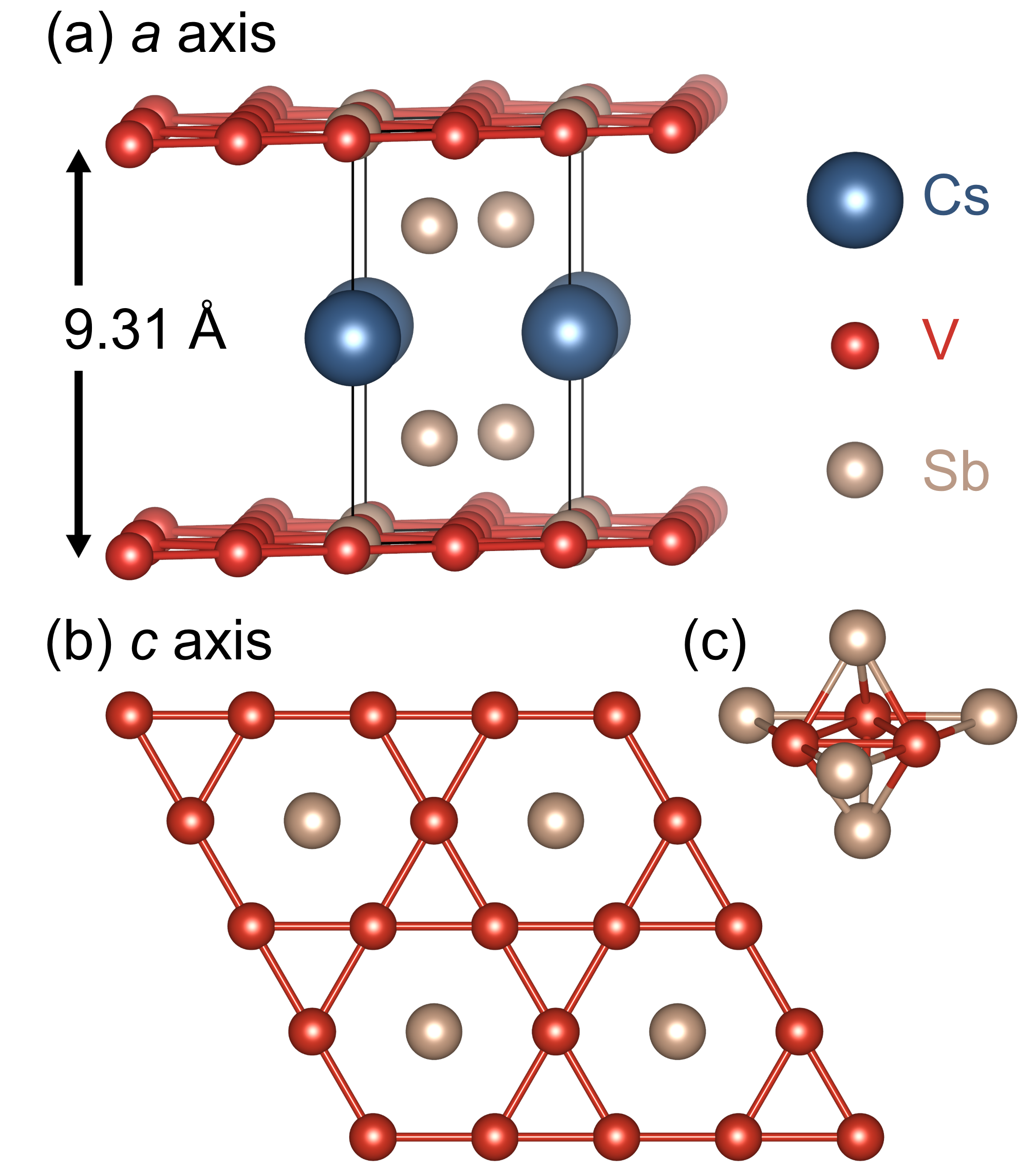
The kagome net of corner-sharing triangles (Figure 1) has drawn significant interest as a platform for a variety of instabilities and emergent phenomena like spin liquid states, superconductivity, charge density waves, and topological surface states.[13, 14, 15] Recently, materials within the AV3Sb5 (A = K, Rb, Cs) kagome family were categorized as topological metals following the Fu-Kane method.[11, 12] The presence of two continuous gaps throughout the BZ near EF allowed for the calculation of multiple invariants, both of which indicated non-trivial topology suggesting that \ceCsV3Sb5 exhibits topological surface states analogous to a topological insulator. This original analysis relied on a band structure that was obtained via a structural relaxation with the PBE functional [16] and D3 correction with the addition of spin-orbit coupling (SOC) in the self-consistent calculation. The D3 correction is an empirical van der Waals total energy correction that was identified as a necessary parameter to more closely match experimental lattice parameters (specifically along the c-axis) during relaxation.[17, 18]
Here, we present electronic structure analysis of \ceCsV3Sb5, with special consideration of anisotropic nonlocal correlation along the kz or inter-kagome-plane direction. Within the framework of density functional theory (DFT), we find that including certain computational parameters during a structural relaxation gives rise to a symmetry-allowed band crossing previously not identified between and A as highlighted in Figure 2. Yet, ultimately, this study suggests that it is critical to include nonlocal and dynamical many-body correlation through the application of the GW approximation to obtain accurate interlayer band behavior. The resulting electronic structure shows significant shifts of the bands and the absence of the symmetry-allowed crossing seen in standard DFT band structures. This seemingly minor detail in the electronic structure impacts the calculation of invariants in this material and points to a larger issue of correct band identification or tracking when plotting band structures.
II Methods
First-principles calculations were performed using the Vienna Ab initio Simulation Package (VASP) version 5.4.4. Pseudopotentials following the projector-augmented wave method were selected with the following valence configurations: Cs (5s25p66s1), V (3s23p64s23d3), Sb (5s25p3). An 11 11 5 -centered k-point mesh was automatically generated by VASP and the plane-wave energy cutoff was set to 500 eV. Geometric optimization of the experimental structure (ICSD 31841) was performed with all parameters in the description (eg. SOC, D3, TS, etc.) unless otherwise stated and all degrees of freedom (atomic positions and cell shape/volume) were allowed to relax until forces were converged within 107 eV/Å. All calculations had an energy convergence better than 108 eV. A k-point path for the band structure was generated using the AFLOW online tool and the density of the path was set 50 k-points per path segment (for example between and A) to ensure high resolution of band features in the final plot.[19] Irreducible representations were obtained using the Irvsp program that interfaces with VASP outputs.[20]
GW calculations implemented in VASP were performed on the experimental (unrelaxed) structure and employed the PBE electronic structure as a starting point. Both single-shot G0W0 and partially self-consistent eigenvalue GW0 (ev GW0) calculations were performed. GW potentials were selected based on the VASP recommendations with the following valence configurations: Cs (5s25p66s1), V (3s23p64s23d3), Sb (4d105s25p3). The total number of bands was set to 4000 and the number of frequency points was set to 100. Given the high computational cost of GW calculations, a smaller 4 4 2 k-point grid was used. This setup yields quasiparticle energies converged to within 50 meV. For the GW0 calculation, seven steps were necessary for convergence, however, all results detailed in this study were taken after ten steps. Since the orbitals are not updated in the ev GW0 self-consistency scheme, the interpolation of bands between and A in the GW output should match that seen in standard DFT even as the eigenvalues are updated. To visualize the resulting band behavior, eigenvalues were matched to the ordering of states in DFT outputs. The interpolation of bands between and A was preserved from the unrelaxed PBE band structure, yet it was scaled such that the endpoint energies (at and A) correspond to the updated eigenvalues from the GW calculations. Further details are provided in the Appendix.
III Results
III.1 General features of the band structure
The electronic structure of \ceCsV3Sb5 hosts a variety of features associated with unique physical phenomena. Many computational efforts have focused on the Dirac crossings [21] and van Hove singularities [22] characteristic of the kagome electronic structure. Specifically, there is significant interest in the near-Fermi-level saddle points in the band structure that correspond to van Hove singularities or divergences in the density of states (DOS). Due to the high DOS, interactions can become pronounced when a saddle point becomes populated and can nest across the Fermi surface. In \ceCsV3Sb5, multiple saddle points residing at the M-point give rise to competing instabilities depending on band filling.[23, 22]
Yet, while the intra-layer interactions draw focus, the interlayer electronic behavior is understudied.[24] Among kagome materials, the 135 family is highly two-dimensional as seen in the stacking of the kagome layers (Figure 1). While these materials are not considered traditional 2D materials given the presence of A-site ions between the layers, previous electronic structure work concluded that van der Waals interactions were necessary to reproduce the experimental c-axis lattice parameter during structural relaxation. These interactions are most relevant along the interlayer or kz direction represented along the -A and K-H paths within the Brillouin zone. The near-Fermi level bands along these paths are dominated by Sb pz-orbitals unlike the V character bands found elsewhere in the BZ.[25]
III.2 Band crossing along -A
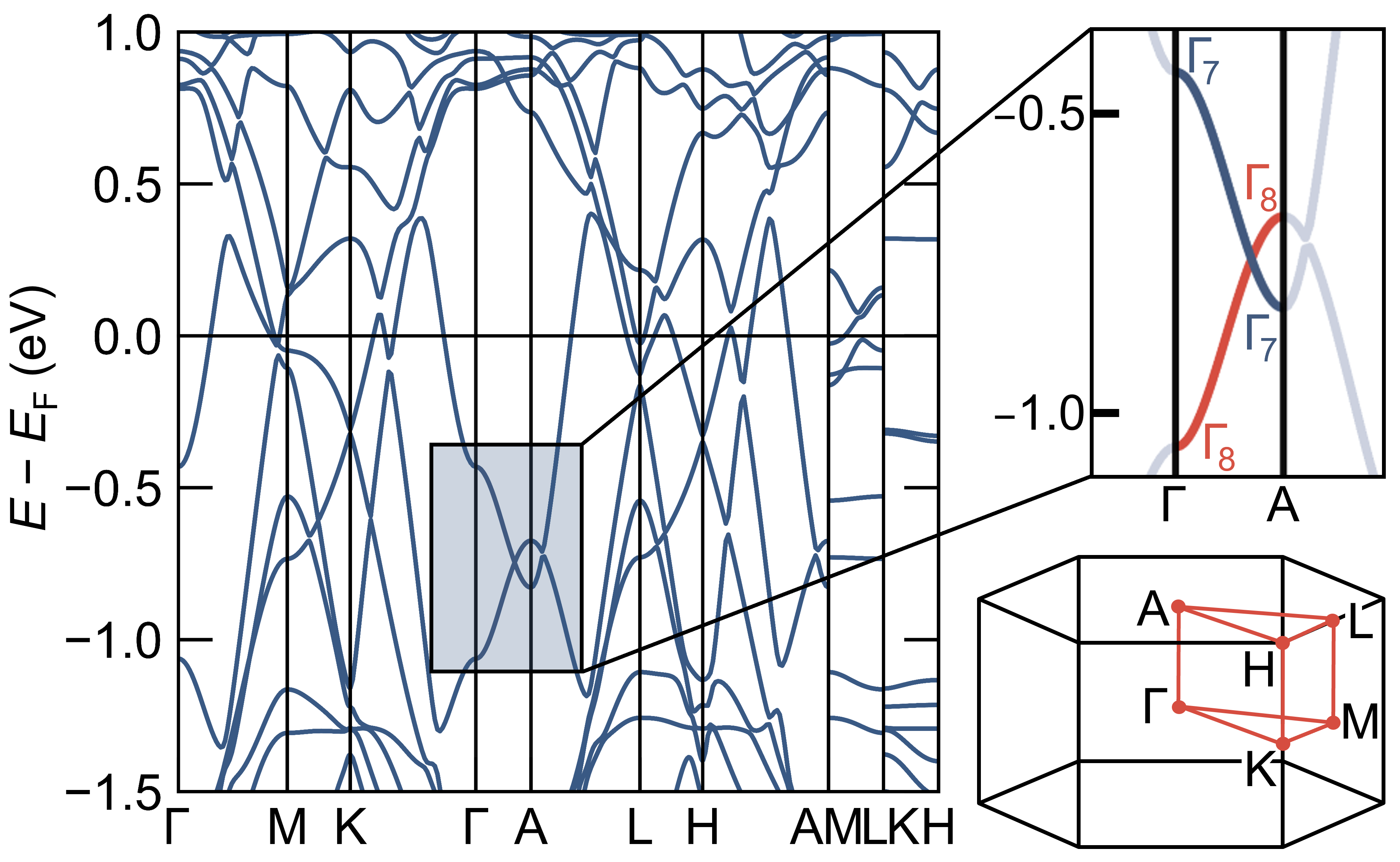
When comparing published band structures for this material, there is a large degree of variability with respect to the band behavior between and A, specifically around 0.75 eV below the Fermi energy. These band structures can be categorized into three main groups depending on the interaction of the two bands in this energy range: 1) fully gapped bands [23, 26, 27], 2) seemingly touching bands with a minor gap [12, 28], and 3) fully crossed bands with crossings between and A and between A and L [29, 30]. We similarly obtain these variations of electronic structures depending on the parameters included in the calculation and the methods employed for plotting. To understand the nature of and potentially validate these crossings, the symmetry or the irreducible representations (irreps) of the bands at specific k-points needs to be analyzed. When bands possess the same symmetry or irrep, the associated electronic states mix or hybridize and form a gap. Only when bands have different irreps can a symmetry-allowed crossing occur.[31]
Irreps additionally change with the inclusion of SOC since a spinor representation (as opposed to a vector representation) is required to capture the spin symmetry. Within the Brillouin zone of \ceCsV3Sb5, most of the paths connecting k-points have C2v symmetry which has only one spinor irrep. Since bands cannot have differing irreps along these paths, there will not be any symmetry-allowed crossings in these areas. However, the paths along -A and K-H have C6v symmetry with multiple spinor irreps allowing for crossings. It is important to note that “symmetry-allowed crossing” does not refer to symmetry-enforced crossings arising from nonsymmorphic symmetries. While the crossings of interest are dictated or “enforced” by the differing symmetries of the bands, we avoid this terminology since it already has a specific definition within topological band theory.[32, 33]
When band symmetry is included in the previously optimized calculations for \ceCsV3Sb5 (relaxed with PBE + D3 followed by PBE + D3 + SOC ground state calculation in [12]), multiple band crossings are observed along -A and K-H. Since the band behavior between and A conflict with previous reports, those crossings are the focus of this study. Based on symmetry considerations, the two bands around 0.75 eV below the Fermi energy cross between and A but are gapped beyond A since they possess the same spinor irrep beyond that k-point. Although these bands are significantly below the Fermi level, they contribute to the characterization of this material and they provide insight into the interlayer electronic behavior.
To identify the origin of this crossing, a series of calculations were performed to track the evolution of the band structure and the relaxed physical structure as summarized in Figure 3. From here on, when referring to electronic structure calculations unless indicated otherwise, this includes a structural relaxation, a self-consistent calculation, followed by band structure and density of states (DOS) calculations in which the Fermi level for the band structure is taken from the DOS calculation given the more accurate sampling of k-points (for more detailed discussion see methods section). Each step in this procedure includes all listed parameters.
When the electronic structure is calculated without the D3 corrections, no band crossing between and A is observed in the energy range of interest. Specifically, the PBE band structure shows clearly gapped bands and the PBE + SOC band structure shows a small gap consistent with irrep analysis. These results indicate that some contribution from the D3 van der Waals correction is responsible for the crossing. To deconvolute whether this contribution is structural i.e. from the relaxation or electronic, the same calculations were performed using the experimental structure without any relaxation. The structurally unrelaxed calculations show the band crossing in the absence of D3, suggesting that the contribution from this correction is structural. In other words, the experimental geometry exhibits an electronic structure with the crossing along -A and the D3 correction maintains this crossing since the relaxed structure most closely matches experimental lattice parameters.
III.3 Comparison of band disperson corrections
It is well documented that DFT methods over-delocalize electrons leading to overly disperse bands.[34, 35] These errors are potentially most pronounced for band dispersions along the out-of-plane direction within quasi-two-dimensional materials like the \ceAV3Sb5 kagomes compounds. Within the Brillouin zone (Figure 2), this direction is represented by the -A, K-H, and M-L paths meaning that these paths are more likely affected by over-dispersion. Since the crossing of interest is along -A, any correction of the band dispersion (i.e. decreasing the bandwidth) could open a gap between the two bands.
To probe the conditions under which a gap might open between the bands and, thereby assess the robustness of this crossing, we compare a variety of commonly applied DFT approaches that address anisotropic nonlocal exchange and correlation at various levels. Again, all parameters or techniques were benchmarked against experimental or unrelaxed results to parse the electronic and structural contributions. Within electronic structure theory, there are a variety of methods to deal with localized electrons including: 1) adding a Hubbard U correction to specific orbitals, 2) adding an energetic correction term, 3) switching to a different exchange-correlation functional, and 4) turning to more advanced methods that more accurately treat band dispersions. While the following results do not constitute an exhaustive selection of all methods impacting band dispersion, a representative set of calculations within all of these categories were performed to provide generalized results as summarized in Figure 3. Methods were selected based on their computational accessibility and the specificity of the correction to the interlayer band dispersion.
Hubbard U corrections are commonly used because they provide a targeted method for dealing with electron over-delocalization usually in d- and f-orbitals in a tunable and computationally inexpensive way.[36, 37, 38, 39] In the context of \ceCsV3Sb5, primarily Sb p-orbitals contribute to the near EF bands at the Brillouin zone center. While p-orbitals typically do not suffer from the same over-delocalization issues in DFT, adding a variable U to these orbitals is a valuable exercise for tracking the behavior of the crossing as a function of the bandwidths of the involved bands. As the value of the U is increased, the deviations along the a- and c-axes become progressively more positive signifying an expansion of the unit cell during relaxation. In the presence of the D3 van der Waals correction, calculations with a Hubbard U from 1 eV to 6 eV exhibit a crossing. Without the D3 correction, these calculations show fully gapped bands with high lattice parameter deviations along the c-axis.
Since \ceCsV3Sb5 is considered a quasi-two-dimensional material given the separation of the kagome layers, van der Waals corrections beyond the D3 term could provide more accurate band dispersions corresponding to localized electrons along the kz direction. These van der Waals terms are total energy corrections that are added to the calculated Kohn-Sham DFT (KS-DFT) energy and, therefore, do not impact the fundamental electronic structure. The computational efficiency of adding these corrections and the relative success in matching experimental lattice parameters make these terms a popular method for addressing van der Waals systems.[40, 41] However, moving to less empirical van der Waals corrections like the Tkatchenko-Sheffler (TS) correction [42] does not yield an improvement in the relaxed lattice parameters. In fact, the c-axis lattice parameter is significantly shorter compared to the experimental value.
Changing the exchange-correlation functional can be a more rigorous method for incorporating dispersion changes within the electronic structure calculation. For example, nonlocal van der Waals density functionals can approximate dispersion interactions by including a nonlocal correlation functional.[43, 44, 45, 46] However, for \ceCsV3Sb5 the selected van der Waals functionals (vdW-DF, optB86b-vdW, SCAN + rVV10) do not perform better than PBE with the D3 total energy correction in reproducing the experimental lattice parameters. Yet, using PBEsol [47], a modification of the PBE functional optimized for extended solids, yielded a relaxed structure with lattice parameters within 2% deviation from the experimental values without the addition of any explicit van der Waals correction.
All of these corrections and methods were additionally compared to unrelaxed calculations (not shown in Figure 3) to deconvolute the structural and electronic contributions. Under all tested computational parameters, a crossing is observed between the Sb bands along -A, pointing to the importance of the structural relaxation in controlling the presence of this crossing.
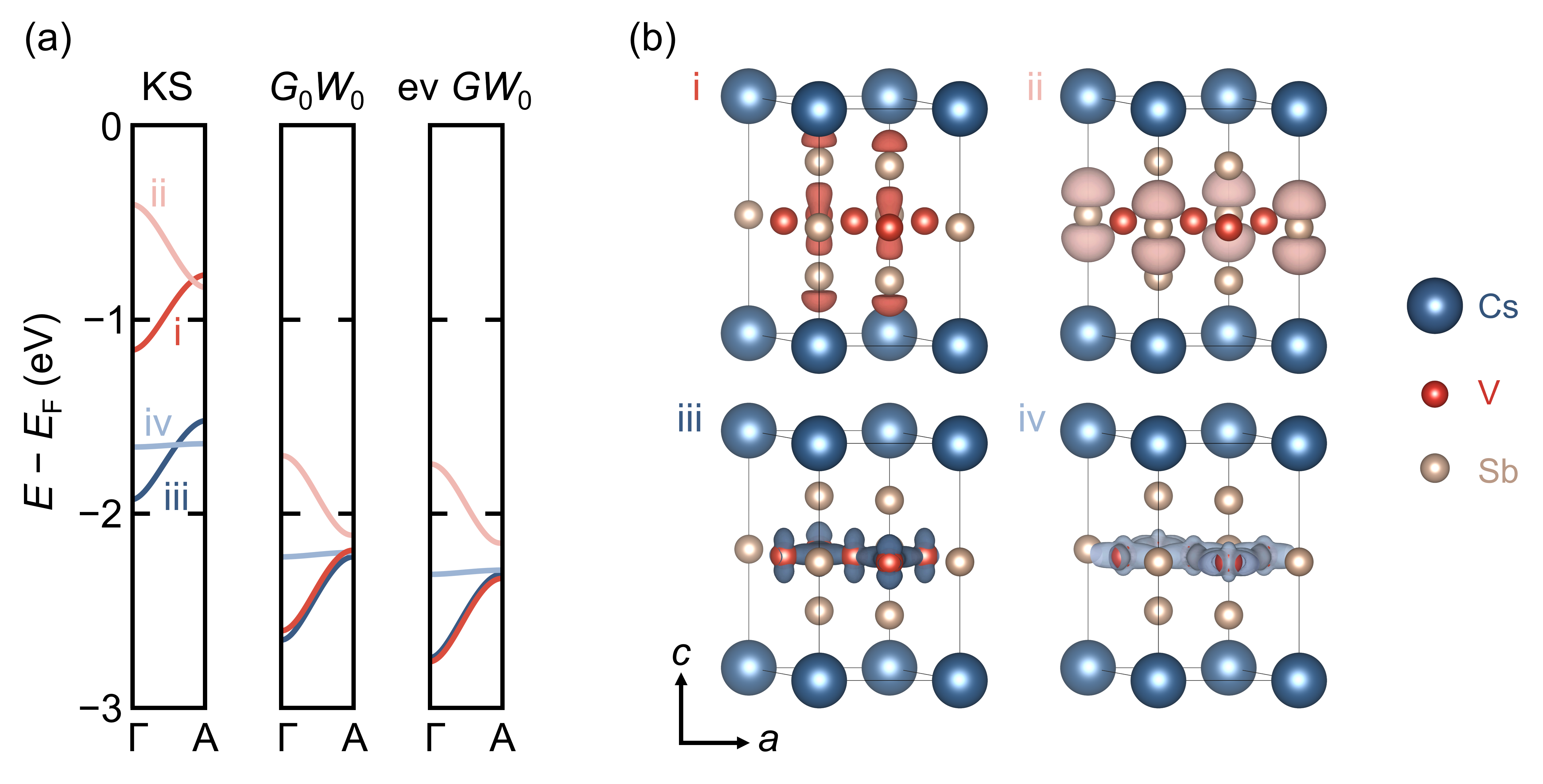
Moving outside of the framework of DFT or coupling DFT results with additional methods can also provide a more accurate picture of the electronic structure. For example, using the GW approximation for the electronic self-energy can appropriately narrow bands by more accurately capturing electron exchange and correlation, however, at higher computational cost. The GW approximation relies on a quasiparticle (QP) picture of the system in which electrons are “dressed” with positively-charged polarization clouds due to the Coulomb repulsion of other electrons. These quasiparticles, which can be described using single-particle Green’s functions (G), interact weakly via a dynamically screened Coulomb potential (W). Typically, GW calculations provide good estimates of the band energies and dispersions when comparing electronic structures from theory and experiment. Since GW calculations capture correlations stemming from dynamical and non-local density fluctuations, these calculations are well-suited for systems in which van der Waals forces play a role. For \ceCsV3Sb5, these types of interactions likely dominate the interlayer electronic behavior, meaning that the GW approximation provides inherent advantages over static mean field methods like KS-DFT.
GW calculations were performed on the experimental structure without SOC and compared to a range of DFT results using the LDA, PBE, SCAN, and nonlocal van der Waals density functionals (vdW-DF, optB86b, SCAN + rVV10).[43, 44, 45, 46, 48] Single-shot G0W0 and partially self-consistent eigenvalue GW0 yield similar band behavior as shown in Figure 4, indicating that single shot calculations will give a relatively consistent picture of the band structure. Based on the partially self-consistent eigenvalue GW0 results, the band dispersions are fairly consistent with a maximum of 12% deviation in the dispersions of the Sb bands. A similar investigation of V bands around 1.7 eV below the Fermi level yield a significantly higher deviation of up to 48%.
While the dispersions of the revelant bands remain relatively consistent when moving to GW calculations, all bands experience significant energy shifts and re-ordering especially below the Fermi level as indicated in Figure 4. In particular, the two Sb bands shift downward by more than 1 eV, combining these bands with lower-lying less-dispersive V bands that experience less than 1 eV shifts downward. This shift induces a reordering of bands as some V bands now lie between the two Sb bands. Quantifying the quasiparticle energy shifts at and A shows larger shifts of around 1.6 eV and 1.3 eV for pz bands associated with Sb outside the kagome layer and within the kagome layer, respectively and smaller shifts of 0.80 eV and 0.65 eV for V dz2 and V dxy/x2y2 bands, respectively. Orbital contributions are attributed based on band-decomposed charge densities depicted in Figure 4b and published electronic structures with orbital projections.[25, 24] The relative energy shifts of bands with varying degrees of interlayer character ultimately results in bands that are fully gapped between and A.
IV Discussion
Within standard DFT, various band dispersion correction terms and methods lead to a similar conclusion: when the structure matches or is comparable to the experimental structure, the associated band structure will feature a symmetry-allowed crossing along -A. This conclusion is evident in calculations where structural relaxations are performed; when there is a small deviation between the relaxed and experimental lattice parameters, a crossing is observed. Unrelaxed calculations reinforce this result by showing a crossing that is robust to a variety of electronic corrections and terms. Additionally, the dispersions of the Sb bands that introduce the crossing are maintained across a variety of functionals and in GW calculations. Yet, in moving to quasiparticle energies, significant energetic shifts are observed. These shifts are more pronounced for bands with higher degrees of interlayer orbital character. For example, the purely intra-layer V dxy/x2y2 bands experience the smallest shift in quasiparticle versus Kohn-Sham energies, whereas the out-of-plane Sb pz band experiences the largest shift. Since the in-plane Sb band does not shift as much as the out-of-plane Sb, a gap is expected to open between these bands (note the separation between bands i and ii in Figure 4).
Based on DFT calculations, the presence of this symmetry-allowed crossing and its robustness with a variety of band dispersion corrections suggests a reevaluation of the electronic structure of \ceCsV3Sb5 specifically along the kz direction. GW calculations provide further insights into the interlayer electronic structure, revealing the absence of this crossing due to significant energetic shifts of bands below the Fermi level. Additionally, these results show interlayer interactions mediated through the V and out-of-plane Sb atoms indicated by the almost degenerate i and iii bands shown in Figure 4. The hybridization of these states suggests more interlayer phenomena at play than indicated in previous electronic structures.
Given the two-dimensionality of this kagome system, it is particularly important to study the interlayer electronic behavior as has been demonstrated computationally and experimentally with effects due to pressure and chemical doping and charge-density wave ordering.[26, 29, 30, 49] All of these phenomena show dramatic changes along the c- or kz-axes pointing to the critical role of understanding interlayer interactions. Rigorous electronic structure calculations capturing the kz dispersion are further necessary since experimental verification of theses bands via ARPES remains challenging. The highly two-dimensional single crystals make it difficult to obtain a clean surface required for the technique along the relevant axis.
Additionally, the -A crossing (or lack thereof) has greater implications in the topological characterization of this system via invariant calculations. A crossing implies the absence of a continuous gap necessary for Fu-Kane calculations across a band manifold. In the case of \ceCsV3Sb5, there is an additional continuous gap throughout the Brillouin zone that interacts with the Fermi level that yields a non-trivial invariant. Since the Fu-Kane method involves taking the product of parity eigenvalues, the ordering of bands below the continuous gap does not affect the overall result meaning that the calculation for this particular gap is unchanged from previous reports even with the band re-ordering along -A seen in the GW results.[12] Ultimately, the presence or absence of this symmetry-allowed crossing does not change the non-trivial classification even though it potentially reduces the number of continuous gaps. However, in other systems that do not have additional continuous gaps, subtle crossings that are not identified until irreps are considered could have more severe consequences on topological invariant calculations.
This study motivates revisiting the protocol for defining invariants in metallic systems. Since the Fu-Kane method was originally intended for insulators, the presence of a gap and, subsequently, a separable band manifold is guaranteed by the system. [7] However, when moving to metals, this condition of separable bands becomes a prerequisite step before continuing with the calculation. From this study of \ceCsV3Sb5, we find that visual identification of a near-Fermi level gap that extends throughout the entire Brillouin zone is not always sufficient fulfillment of this prerequisite. Our results highlight the importance of confirming a gap via irreps prior to performing analysis in metals.
Finally, broader lessons regarding the interpretation of band structures can be learned from this study of \ceCsV3Sb5. For example, recognizing that most band structure outputs do not include band symmetries and can, therefore, misidentify “continuous” bands advocates the integration of irrep analysis when depicting and understanding band structures. This lack of proper band tracking is reinforced if other computational parameters like k-point density along the Brillouin zone path are not high enough to resolve small features. These issues are crucial when attempting to calculate topological invariants based on bulk band structures but are also widely applicable to any system in which an accurate picture of the electronic structure is necessary.
V Conclusion
Using first-principles calculations, we have identified new band behavior along the interlayer direction in \ceCsV3Sb5. Given the two-dimensional nature of this system, capturing the electronic structure along the c- or kz-direction is experimentally and computationally difficult. In this study, we survey a variety of computational methods to address nonlocal exchange and correlation at different scales. Density functional theory calculations show a symmetry-allowed crossing along the kz-dispersion that arises due to the structural contribution of dispersion corrections and methods employed during relaxation to more closely match experimental lattice parameters. This crossing is revealed upon irrep analysis of the bands. Yet, in turning towards dynamical nonlocal correlation via GW calculations, this crossing is absent due to relative energy shifts of bands with varying interlayer character. The resulting kz electronic structure points to increased interactions occurring out of the kagome plane and serves as a baseline band structure for further studies of inter-kagome-layer phenomena.
VI Acknowledgments
We thank J. W. Harter, L. Balents, M. G. Vergniory, and I. Robredo for helpful discussions and feedback. This work was supported by the National Science Foundation (NSF) through Enabling Quantum Leap: Convergent Accelerated Discovery Foundries for Quantum Materials Science, Engineering and Information (Q-AMASE-i): Quantum Foundry at UC Santa Barbara (DMR 1906325). Additionally, we thank NSF CAREER award DMR 1945098. We also acknowledge the use of computational facilities administered by the Center for Scientific Computing at UC Santa Barbara supported by NSF CNS 1725797 and NSF DMR 2308708.
*
Appendix A Plotting electronic structures
Since typical band structure data include the k-points and energies of each band, portions of this data need to be rearranged to reflect the true band identity confirmed by irreps. For example, if two bands cross between k-point 1 and k-point 2, the output may incorrectly identify all lower energies as a continuous band and similarly all higher energies as another continuous band. In other words, the lower energy band before the crossing will be spuriously connected to the lower energy band after the crossing. However, looking at the irreps at k-point 1 and k-point 2 will indicate there is a crossing because the irreps switch between the two k-points. This weakness in the output can be corrected by identifying the point at which the crossing occurs and reconnecting the bands to match the irrep results. This practice can be seen in Figure 2 where the bands between and A have been reconnected and colored to match the irreps.
The GW band structures in Figure 4 were constructed based on the unrelaxed PBE band structure. Once the bands were reconnected based on irreps, each band was rescaled and repositioned according to the renormalization computed in the G0W0 and GW0 calculations at and at A. As such, bands from the GW output may suffer from the same misidentification across crossings, however since only the energies and not the orbitals are updated in the employed partially self-consistent scheme, the GW energies can be properly matched based on the ordering of bands from the original PBE band structure.
References
- Xiao and Yan [2021] J. Xiao and B. Yan, First-principles calculations for topological quantum materials, Nat. Rev. Phys. 3, 283 (2021).
- Bradlyn et al. [2017] B. Bradlyn, L. Elcoro, J. Cano, M. G. Vergniory, Z. Wang, C. Felser, M. I. Aroyo, and B. A. Bernevig, Topological quantum chemistry, Nature 547, 298 (2017).
- Bansil et al. [2016] A. Bansil, H. Lin, and T. Das, Colloquium: Topological band theory, Rev. Mod. Phys. 88 (2016).
- Kane and Mele [2005] C. L. Kane and E. J. Mele, Z2 Topological Order and the Quantum Spin Hall Effect, Phys. Rev. Lett. 95 (2005).
- Fu et al. [2007] L. Fu, C. L. Kane, and E. J. Mele, Topological Insulators in Three Dimensions, Phys. Rev. Lett. 98 (2007).
- Moore and Balents [2007] J. E. Moore and L. Balents, Topological invariants of time-reversal-invariant band structures, Phys. Rev. B 75 (2007).
- Fu and Kane [2007] L. Fu and C. L. Kane, Topological insulators with inversion symmetry, Phys. Rev. B 76, 045302 (2007).
- Schoop et al. [2015] L. M. Schoop, L. S. Xie, R. Chen, Q. D. Gibson, S. H. Lapidus, I. Kimchi, M. Hirschberger, N. Haldolaarachchige, M. N. Ali, C. A. Belvin, T. Liang, J. B. Neaton, N. P. Ong, A. Vishwanath, and R. J. Cava, Dirac metal to topological metal transition at a structural phase change in Au2Pb and prediction of Z2 topology for the superconductor, Phys. Rev. B 91, 214517 (2015).
- Qian et al. [2022] J. Qian, Z. Shen, X. Wei, and W. Li, Z2 nontrivial topology of rare-earth binary oxide superconductor LaO, Phys. Rev. B 105 (2022).
- Nayak et al. [2017] J. Nayak, S.-C. Wu, N. Kumar, C. Shekhar, S. Singh, J. Fink, E. E. D. Rienks, G. H. Fecher, S. S. P. Parkin, B. Yan, and C. Felser, Multiple dirac cones at the surface of the topological metal LaBi, Nat. Commun. 8 (2017).
- Ortiz et al. [2021] B. R. Ortiz, P. M. Sarte, E. M. Kenney, M. J. Graf, S. M. L. Teicher, R. Seshadri, and S. D. Wilson, Superconductivity in the Z2 kagome metal KV3Sb5, Phys. Rev. Mater. 5, 034801 (2021).
- Ortiz et al. [2020] B. R. Ortiz, S. M. Teicher, Y. Hu, J. L. Zuo, P. M. Sarte, E. C. Schueller, A. M. Abeykoon, M. J. Krogstad, S. Rosenkranz, R. Osborn, R. Seshadri, L. Balents, J. He, and S. D. Wilson, CsV3Sb5 : A Z2 Topological Kagome Metal with a Superconducting Ground State, Phys. Rev. Lett. 125, 247002 (2020).
- Yan et al. [2011] S. Yan, D. A. Huse, and S. R. White, Spin-Liquid Ground State of the S = 1/2 Kagome Heisenberg Antiferromagnet, Science 332, 1173 (2011).
- Ko et al. [2009] W.-H. Ko, P. A. Lee, and X.-G. Wen, Doped kagome system as exotic superconductor, Phys. Rev. B 79 (2009).
- Guo and Franz [2009] H.-M. Guo and M. Franz, Topological insulator on the kagome lattice, Phys. Rev. B 80 (2009).
- Perdew et al. [1996] J. P. Perdew, K. Burke, and M. Ernzerhof, Generalized Gradient Approximation Made Simple, Phys. Rev. Lett. 77, 3865 (1996).
- Grimme et al. [2010] S. Grimme, J. Antony, S. Ehrlich, and H. Krieg, A consistent and accurate ab initio parametrization of density functional dispersion correction (DFT-D) for the 94 elements H-Pu, J. Chem. Phys. 132, 154104 (2010).
- Grimme et al. [2011] S. Grimme, S. Ehrlich, and L. Goerigk, Effect of the damping function in dispersion corrected density functional theory, J. Comput. Chem. 32, 1456 (2011).
- Curtarolo et al. [2012] S. Curtarolo, W. Setyawan, G. L. Hart, M. Jahnatek, R. V. Chepulskii, R. H. Taylor, S. Wang, J. Xue, K. Yang, O. Levy, M. J. Mehl, H. T. Stokes, D. O. Demchenko, and D. Morgan, AFLOW: An automatic framework for high-throughput materials discovery, Comput. Mater. Sci. 58, 218 (2012).
- Gao et al. [2021] J. Gao, Q. Wu, C. Persson, and Z. Wang, Irvsp: To obtain irreducible representations of electronic states in the VASP, Comput. Phys. Commun. 261, 107760 (2021).
- Hao et al. [2022] Z. Hao, Y. Cai, Y. Liu, Y. Wang, X. Sui, X.-M. Ma, Z. Shen, Z. Jiang, Y. Yang, W. Liu, Q. Jiang, Z. Liu, M. Ye, D. Shen, Y. Liu, S. Cui, J. Chen, L. Wang, C. Liu, J. Lin, J. Wang, B. Huang, J.-W. Mei, and C. Chen, Dirac nodal lines and nodal loops in the topological kagome superconductor CsV3Sb5, Phys. Rev. B 106 (2022).
- Hu et al. [2022] Y. Hu, S. M. Teicher, B. R. Ortiz, Y. Luo, S. Peng, L. Huai, J. Ma, N. C. Plumb, S. D. Wilson, J. He, and M. Shi, Topological surface states and flat bands in the kagome superconductor CsV3Sb5, Sci. Bull. 67, 495 (2022).
- Kang et al. [2022] M. Kang, S. Fang, J.-K. Kim, B. R. Ortiz, S. H. Ryu, J. Kim, J. Yoo, G. Sangiovanni, D. D. Sante, B.-G. Park, C. Jozwiak, A. Bostwick, E. Rotenberg, E. Kaxiras, S. D. Wilson, J.-H. Park, and R. Comin, Twofold van Hove singularity and origin of charge order in topological kagome superconductor CsV3Sb5, Nat. Phys. 18, 301 (2022).
- Tsirlin et al. [2022] A. Tsirlin, P. Fertey, B. R. Ortiz, B. Klis, V. Merkl, M. Dressel, S. Wilson, and E. Uykur, Role of Sb in the superconducting kagome metal CsV3Sb5 revealed by its anisotropic compression, SciPost Phys. 12 (2022).
- Li et al. [2022] C. Li, X. Wu, H. Liu, C. Polley, Q. Guo, Y. Wang, X. Han, M. Dendzik, M. H. Berntsen, B. Thiagarajan, Y. Shi, A. P. Schnyder, and O. Tjernberg, Coexistence of two intertwined charge density waves in a kagome system, Phys. Rev. Res. 4 (2022).
- Oey et al. [2022] Y. M. Oey, B. R. Ortiz, F. Kaboudvand, J. Frassineti, E. Garcia, R. Cong, S. Sanna, V. F. Mitrović, R. Seshadri, and S. D. Wilson, Fermi level tuning and double-dome superconductivity in the kagome metal CsV3Sb5-xSnx, Phys. Rev. Mater. 6 (2022).
- Huang et al. [2022] X. Huang, C. Guo, C. Putzke, M. Gutierrez-Amigo, Y. Sun, M. G. Vergniory, I. Errea, D. Chen, C. Felser, and P. J. W. Moll, Three-dimensional Fermi surfaces from charge order in layered CsV3Sb5, Phys. Rev. B 106 (2022).
- Uykur et al. [2021] E. Uykur, B. R. Ortiz, O. Iakutkina, M. Wenzel, S. D. Wilson, M. Dressel, and A. A. Tsirlin, Low-energy optical properties of the nonmagnetic kagome metal CsV3Sb5, Phys. Rev. B 104 (2021).
- Chen et al. [2021] K. Chen, N. Wang, Q. Yin, Y. Gu, K. Jiang, Z. Tu, C. Gong, Y. Uwatoko, J. Sun, H. Lei, J. Hu, and J.-G. Cheng, Double Superconducting Dome and Triple Enhancement of Tc in the Kagome Superconductor CsV3Sb5 under High Pressure, Phys. Rev. Lett. 126 (2021).
- Yu et al. [2022] F. Yu, X. Zhu, X. Wen, Z. Gui, Z. Li, Y. Han, T. Wu, Z. Wang, Z. Xiang, Z. Qiao, J. Ying, and X. Chen, Pressure-Induced Dimensional Crossover in a Kagome Superconductor, Phys. Rev. Lett. 128 (2022).
- Dresselhaus et al. [2008] M. S. Dresselhaus, G. Dresselhaus, and A. Jorio, Group Theory: Application to the Physics of Condensed Matter (Springer-Verlag Berlin Heidelberg, 2008) pp. 305–336.
- Zhao and Schnyder [2016] Y. X. Zhao and A. P. Schnyder, Nonsymmorphic symmetry-required band crossings in topological semimetals, Phys. Rev. B 94 (2016).
- Hirschmann et al. [2021] M. M. Hirschmann, A. Leonhardt, B. Kilic, D. H. Fabini, and A. P. Schnyder, Symmetry-enforced band crossings in tetragonal materials: Dirac and Weyl degeneracies on points, lines, and planes, Phys. Rev. Mater. 5 (2021).
- Sholl and Steckel [2009] D. S. Sholl and J. A. Steckel, Density Functional Theory: A Practical Introduction (Wiley, 2009) pp. 209–233.
- Martin [2004] R. R. Martin, Electronic Structure: Best Theory and Practical Methods (Cambridge University Press, 2004) pp. 152–171.
- Anisimov et al. [1991] V. I. Anisimov, J. Zaanen, and O. K. Andersen, Band theory and Mott insulators: Hubbard U instead of Stoner I, Phys. Rev. B 44, 943 (1991).
- Cococcioni and de Gironcoli [2005] M. Cococcioni and S. de Gironcoli, Linear response approach to the calculation of the effective interaction parameters in the LDA + U method, Phys. Rev. B 71 (2005).
- Kulik [2015] H. J. Kulik, Perspective: Treating electron over-delocalization with the DFT+U method, J. Chem. Phys. 142, 240901 (2015).
- Dudarev et al. [1998] S. L. Dudarev, G. A. Botton, S. Y. Savrasov, C. J. Humphreys, and A. P. Sutton, Electron-energy-loss spectra and the structural stability of nickel oxide: An LSDA+U study, Phys. Rev. B 57, 1505 (1998).
- Reckien et al. [2012] W. Reckien, F. Janetzko, M. F. Peintinger, and T. Bredow, Implementation of empirical dispersion corrections to density functional theory for periodic systems, J. Comput. Chem. 33, 2023 (2012).
- Grimme et al. [2016] S. Grimme, A. Hansen, J. G. Brandenburg, and C. Bannwarth, Dispersion-Corrected Mean-Field Electronic Structure Methods, Chem. Rev. 116, 5105 (2016).
- Tkatchenko and Scheffler [2009] A. Tkatchenko and M. Scheffler, Accurate Molecular Van Der Waals Interactions from Ground-State Electron Density and Free-Atom Reference Data, Phys. Rev. Lett. 102 (2009).
- Román-Pérez and Soler [2009] G. Román-Pérez and J. M. Soler, Efficient Implementation of a van der Waals Density Functional: Application to Double-Wall Carbon Nanotubes, Phys. Rev. Lett. 103 (2009).
- Dion et al. [2004] M. Dion, H. Rydberg, E. Schröder, D. C. Langreth, and B. I. Lundqvist, Van der Waals Density Functional for General Geometries, Phys. Rev. Lett. 92 (2004).
- Peng et al. [2016] H. Peng, Z.-H. Yang, J. P. Perdew, and J. Sun, Versatile van der Waals Density Functional Based on a Meta-Generalized Gradient Approximation, Phys. Rev. X 6 (2016).
- Klimeš et al. [2011] J. Klimeš, D. R. Bowler, and A. Michaelides, Van der Waals density functionals applied to solids, Phys. Rev. B 83 (2011).
- Perdew et al. [2008] J. P. Perdew, A. Ruzsinszky, G. I. Csonka, O. A. Vydrov, G. E. Scuseria, L. A. Constantin, X. Zhou, and K. Burke, Restoring the Density-Gradient Expansion for Exchange in Solids and Surfaces, Phys. Rev. Lett. 100 (2008).
- Sun et al. [2015] J. Sun, A. Ruzsinszky, and J. Perdew, Strongly Constrained and Appropriately Normed Semilocal Density Functional, Phys. Rev. Lett. 115 (2015).
- Kautzsch et al. [2023] L. Kautzsch, B. R. Ortiz, K. Mallayya, J. Plumb, G. Pokharel, J. P. C. Ruff, Z. Islam, E.-A. Kim, R. Seshadri, and S. D. Wilson, Structural evolution of the kagome superconductors AV3Sb5 (A = K, Rb, and Cs) through charge density wave order, Phys. Rev. Mater. 7 (2023).