From 3D to 5D tracking: SMX ASIC-based Double-Sided Micro-Strip detectors for comprehensive space, time, and energy measurements
Abstract
We present the recent development of a lightweight detector capable of accurate spatial, timing, and amplitude resolution of charged particles. The technology is based on double-sided double-metal p+ – n – n+ micro-strip silicon sensors, ultra-light long aluminum-polyimide micro-cables for the analogue signal transfer, and a custom-developed SMX read-out ASIC capable of measurement of the time () and amplitude. Dense detector integration enables a material budget . A sophisticated powering and grounding scheme keeps the noise under control.
In addition to its primary application in Silicon Tracking System of the future CBM experiment in Darmstadt, our detector will be utilized in other research applications.
1 Introduction: Silicon Tracking System of the CBM experiment
The Silicon Tracking System (STS) of the Compressed Baryonic Mater (CBM) experiment is the core application and main motivation for the detector technology described in this paper.
CBM is a fixed-target heavy-ion experiment of the future Facility for Antiproton and Ion Research (FAIR) complex in Darmstadt, Germany; it is dedicated to study the strongly interacting matter under extreme conditions [1].
The CBM detector is a single-arm forward spectrometer capable of collecting data in a free-streaming mode to process the unprecedented beam-target interaction rates of up to . The detector will utilise the heavy-ion and proton beams from the SIS-100 accelerator at energies of up to and [2].
STS is the core tracking detector of CBM. Its 8 tracking stations (876 detector modules, total silicon area about ) will be placed downstream of the target in the aperture of the superconductive dipole. The primary goals of the STS are tracking of charged particles ( tracks in the Au+Au central collision), momentum determination with and secondary vertex reconstruction. For these tasks STS requires a position resolution better than in the bending plane, a good time resolution (in the order of ) and a material budget within per tracking station [3, 4, 5, 6].
2 Micro-strip Silicon module: the fundamental functioning block of STS
A key component of the STS detector module is the custom STS-MUCH-XYTER (SMX) Application-Specific Integrated Circuit (ASIC) developed for the front-end electronics of the STS and Muon Chamber (MUCH) detectors of CBM. It features 128 channels each capable of simultaneous measurement of the signal amplitude and time with 5-bit ADC (dynamic range for the STS and for MUCH modes) and 14-bit TDC () in a free-streaming mode [7].
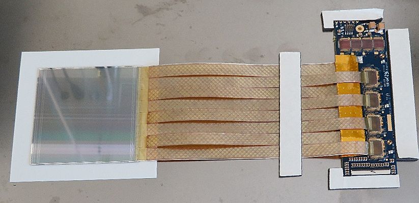
An STS detector module consists of a thick, wide p+ – n – n+ double-sided double-metal (DSDM) silicon microstrip sensor of four versions: , , and long. The sensors are manufactured by Hamamatsu Photonics [8] using high-resistance silicon wafers: typical dark current is at [9, 10, 11]. All sensors underwent an automatised optical inspection [12]. There are strips with a pitch of on each side; the p-side strips are inclined with respect to the side edge at an angle of . The AC readout pads are located in two rows on the top and bottom of the sensor. Each sensor is connected to two front-end boards (FEBs), each containing eight SMX ASICs, via 32 custom ultra-lightweight aluminium-polyimide microcables up to long with the contribution to the material budget per module [13]. A picture of the module during its assembling at GSI Detector Laboratory is shown in figure 1. More details concerning the module structure, construction, calibration and operation can be found in ref. [14].
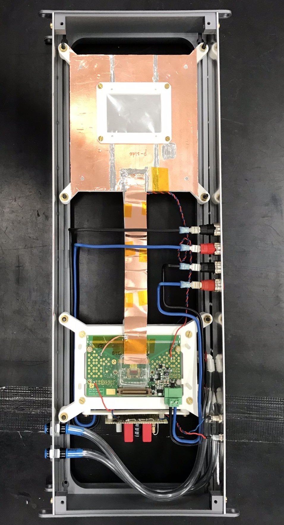
Several versions of the detector Front-End Boards (FEB) were used during the setup developments: from the single-ASIC FEB-C (visible as a part of the prototype module in figure 2, left) to the present date FEB8 (part of the E16 STS module in figure 1). An alternative implementation of the SMX-based silicon micro-strip detector with few alternative FEB form-factors was done for the Strasse tracker [15].
To achieve the expected noise level during operation, the STS module implements a sophisticated ground and powering scheme. This is an important feature addressed in ref. [16]. The HV and ground stability issues are also studied in ref. [17].
The Data Acquisition (DAQ) system of the STS detector together with other CBM subsystems feature radiation hard GBTx and Versatile Link based readout: details on the system architecture, protocol and particular implementations are provided in refs. [18] and [19]. An alternative DAQ chain with commercial off-the-shelf components based on the GBTx-EMU is described in ref. [20]
3 Present and future detector applications
A few dozens of prototype and pre-series modules has been assembled since 2018 [14]. They were involved in multiple laboratory studies and beam tests, primarily with protons at COSY synchrotron (see dedicated chapters of refs. [21, 22]) and heavy-ion collisions in mCBM at SIS18 [23].
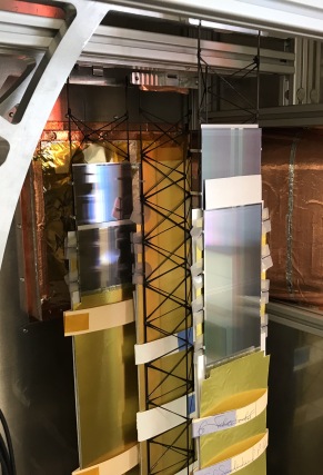
The mSTS detector is a fully-integrated functional STS prototype featuring eleven DSDM silicon strip modules of different sensor sizes (see figure 2, center); it is a part of the mCBM test setup [25]. The mSTS detector was first proposed in 2017 as a part of the installation of the FAIR Phase 0 mCBM experiment which aim to prove the free-streaming DAQ and online reconstruction concept of CBM using high rate nucleus-nucleus collisions at SIS18 synchrotron. Since that time the mSTS setup went through two successful beam campaigns in 2018–2019 and 2020–2022 [26].
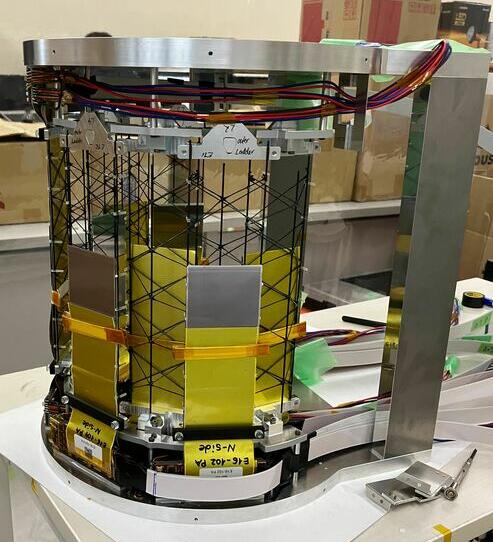
The E16 experiment at J-PARC aims to study in-medium modification of the vector mesons , , and , decaying via channel, with a high-intensity proton beam interacting with a C target and Cu targets at rates up to . It went through three commissioning runs in 2020–2021. Recently, the silicon strip detector was upgraded by replacing older silicon sensors with new ten STS modules built with sensors (see figure 2, right) [27]; it features the GBTx-EMU based DAQ chain [28].
4 Spatial resolution
High spacial resolution and detection efficiency are prime objectives of the tracking detectors. According to simulations performed in ref. [29], and single-hit efficiency were obtained. Preliminary analysis of the mSTS data supports these estimates.
5 Timing and rate capabilities
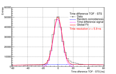
Timing performance of the STS detector modules was measured in several beam tests with relativistic particles. Time resolution of was obtained with a proton beam of at COSY synchrotron (see figure 3, left) [22]. Comparable results were obtained with the mCBM data using the prototype Time-of-Flight detector (TOF) as a reference (see figure 3, right) [23].
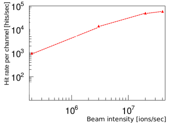
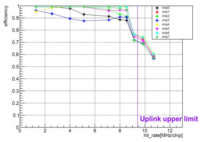
Several independent studies were conducted to establish the signal rate capabilities of the STS modules: beam tests with mSTS so far showed rate capabilities up to (figure 4, left); meantime, E16 team showed stable hit transmission up to with the digitally periodically generated SMX hits (figure 4, right).
6 Energy measurements
Energy loss by a relativistic charge particle penetrating a thin detector follows Landau-Vavilov distribution [30, 31]. The width factors and , and most probable value are usually used to describe the width and the position of Landau-Vavilov distribution; they both depend on the thickness and material of the detector [32]. With the mean energy loss of a minimum ionizing particle (MIP) being we estimate [32], [33], and [34] for MIP in silicon. With the mean energy for electron-hole pair production in silicon [33], the most-probable charge deposition is .
Taking into account the Poisson distribution for the electron-hole creation and a Fano factor for silicon [35], we can finally estimate a typical variation of the charge deposit in the detector:
| (6.1) |
The SMX chip allows us to measure the charge deposited in the micro-strip silicon sensor with its slow channel and 5-bit flash ADC: thus, assuming only perpendicular tracks resulting in uniquely one-strip clusters and dynamic range of the charge uncertainty resulting from the amplitude discretization is about:
| (6.2) |
which is smaller than uncertainty resulting from the conservative estimate of the effective noise charge (ENC) of from ref. [14]:
| (6.3) |
Comparing equations 6.2 and 6.3 to equation 6.1 one can see that the measurement precision is dominated by the nature of the interaction rather than by the read-out electronics.
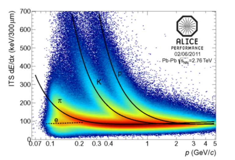
Particle Identification (PID) using the charged particle energy deposition per unit length of detector material (specific energy loss) is a widely used approach in particle and nuclear physics. Heavy-ion experiments typically use information about the continuous energy loss in their gaseous trackers [36, 37]. To some extent, this approach is also applicable to silicon tracking detectors, as has been shown with data from the CMS Tracker [38] and ALICE ITS (see figure 5, left) [37, 39].
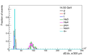
Independent measurements of the energy deposit in multiple tracking stations require averaging. As the arithmetic mean does not reduce the uncertainty, CMS Tracker team uses , while ALICE ITC team uses a truncated mean. We obtained the best results using the median energy value; the bands of the median energy deposits for various particles are shown in figure 5, right.
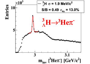
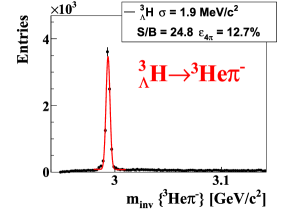
Applying a simple threshold of on the median charge deposited in STS detectors results in almost complete separation of double-charged particles from single-charged particles in the STS [41]. According to CBM simulations, in the case of hyper tritium decay it helped to increase the signal purity by a factor of 50, as shown in Fig.6: the main contamination in this channel are misidentified protons and deuterons, which are overlapped with helium isotopes in TOF detector data [40].
Acknowledgments
This research would not be possible without the contribution made by the engineers and technical staff of the GSI Detector Laboratory, Module Assembling Team: C. Simons, R. Visinka, O. Bertini, K. Schuenemann and O. Suddia. We are grateful to our colleagues at the Karlsruhe Institute of Technology, who have contributed to the production of the modules: T. Blank, H. Herzenstiel, B. Leyrer. Finally, we thank R. Kappel, I. Keshelashvili, and F. Nickels for their valuable inputs.
References
- [1] K. Agarwal, The compressed baryonic matter (CBM) experiment at FAIR – physics, status and prospects, Physica Scripta (2023) .
- [2] M. Durante, P. Indelicato, B. Jonson, V. Koch, K. Langanke, U.-G. Meißner et al., All the fun of the FAIR: fundamental physics at the facility for antiproton and ion research, Physica Scripta 94 (2019) 033001.
- [3] A. Lymanets, The silicon tracking system of the CBM experiment at FAIR, Ukrainian Journal of Physics 64 (2019) 607.
- [4] E. Lavrik, The silicon tracking system of the CBM experiment at FAIR, Journal of Physics: Conference Series 1390 (2019) 012114.
- [5] H. Schmidt, The silicon tracking system of the CBM experiment at FAIR, Nuclear Instruments and Methods in Physics Research Section A: Accelerators, Spectrometers, Detectors and Associated Equipment 936 (2019) 630.
- [6] A. Rodriguez Rodriguez, The silicon tracking system of CBM: towards tests with heavy ion collisions, in 2019 IEEE Nuclear Science Symposium and Medical Imaging Conference (NSS/MIC), IEEE, oct, 2019, DOI.
- [7] K. Kasinski, A. Rodriguez-Rodriguez, J. Lehnert, W. Zubrzycka, R. Szczygiel, P. Otfinowski et al., Characterization of the STS/MUCH-XYTER2, a 128-channel time and amplitude measurement IC for gas and silicon microstrip sensors, Nuclear Instruments and Methods in Physics Research Section A: Accelerators, Spectrometers, Detectors and Associated Equipment 908 (2018) 225.
- [8] “Hamamatsu Photonics https://www.hamamatsu.com/.”
- [9] I. Momot, M. Teklishyn, A. Lymanets, O. Bertini and J. Heuser, Investigation into the charge collection efficiency of prototype microstrip sensors for the CBM silicon tracking system, Journal of Physics: Conference Series 1024 (2018) 012004.
- [10] I. Momot, Characterization and radiation hardness studies of the silicon microstrip sensors for the CBM experiment, Ph.D. thesis, Goethe U., Frankfurt (main), 2019.
- [11] I. Panasenko, Development of Electrical Quality Assurance Procedures and Methods for the Silicon Tracking System of the CBM Experiment, Ph.D. thesis, Eberhard Karls Universität Tübingen, 2022.
- [12] E. Lavrik, M. Shiroya, H. Schmidt, A. Toia and J. Heuser, Optical inspection of the silicon micro-strip sensors for the CBM experiment employing artificial intelligence, Nuclear Instruments and Methods in Physics Research Section A: Accelerators, Spectrometers, Detectors and Associated Equipment 1021 (2022) 165932.
- [13] M. Protsenko, The technology for the production of radiation detector modules, Ph.D. thesis, Kharkiv National University of Radioelectronics, 2017.
- [14] A.R. Rodríguez, O.M. Rodríguez, J. Lehnert, A. Toia, M. Teklishyn, A. Lymanets et al., Functional characterization of modules for the silicon tracking system of the CBM experiment, Nuclear Instruments and Methods in Physics Research Section A: Accelerators, Spectrometers, Detectors and Associated Equipment 1058 (2024) 168813.
- [15] A. Frotscher, The (p,3p) two-proton removal from neutron-rich nuclei and the development of the STRASSE tracker, Ph.D. thesis, Technische Universität Darmstadt, Darmstadt, November, 2021. https://doi.org/10.26083/tuprints-00019806.
- [16] P. Koczon, C.J. Schmidt, U. Frankenfeld, R. Kapell, J. Lehnert, A. Lymanets et al., The powering concept of the Silicon Tracking System for CBM@FAIR, PoS 370 (2020) 063.
- [17] O. Kshyvanskyi, Evaluation of the prototypes of the detector modules for theCBM Silicon Tracking System, Master’s thesis, Taras Shevchenko National University of Kyiv, 2022.
- [18] J. Lehnert, A. Byszuk, D. Emschermann, K. Kasinski, W. Müller, C. Schmidt et al., GBT based readout in the CBM experiment, Journal of Instrumentation 12 (2017) C02061.
- [19] CBM Collaboration, Technical Design Report for the CBM Online Systems – Part I, DAQ and FLES Entry Stage, GSI Helmholtzzentrum fuer Schwerionenforschung, GSI, Darmstadt (2023), 10.15120/GSI-2023-00739.
- [20] W. Zabołotny, D. Emschermann, M. Gumiński, M. Kruszewski, J. Lehnert, P. Miedzik et al., SMX and front-end board tester for CBM readout chain, Journal of Instrumentation 17 (2022) C04030.
- [21] A.R. Rodriguez, The CBM Silicon Tracking System front-end electronics: from bare ASIC to detector characterization, commissioning and performance, doctoralthesis, Goethe U., Frankfurt (main), 2020.
- [22] P. Pfistner, Development of Electrical Quality Assurance Procedures and Methods for the Silicon Tracking System of the CBM Experiment, Ph.D. thesis, Karlsruher Instituts für Technologie, 2021.
- [23] O. Maragoto Rodriguez, Characterization and commissioning of the front-end electronics for the Silicon Tracking System of the CBM experiment, Ph.D. thesis, Goethe U., Frankfurt (main), 2023.
- [24] “J-PARC E16 experiment https://ribf.riken.jp/~yokkaich/E16/E16-index.html.”
- [25] CBM Collaboration, mCBM@SIS18, Darmstadt : CBM Collaboration (2017) GSI 58 S. (2017).
- [26] GSI Helmholtzzentrum für Schwerionenforschung, Darmstadt and FAIR GmbH, Darmstadt, ed., GSI-FAIR Scientific Report 2022, vol. GSI Report 2023-1, GSI Helmholtzzentrum fuer Schwerionenforschung, GSI, Darmstadt (2023), 10.15120/GSI-2023-00462.
- [27] K. Aoki, D. Arimizu, S. Ashikaga, W.-C. Chang, T. Chujo, K. Ebata et al., Experimental Study of In-medium Spectral Change of Vector Mesons at J-PARC, Few-Body Systems 64 (2023) .
- [28] K. Yamaguchi, Development of Readout Circuit for Silicon Strip Detector for Track Detection in J-PARC E16 Experiment, Master’s thesis, Kyoto University, 2022.
- [29] H. Malygina and V. Friese, A precision device needs precise simulation: Software description of the CBM Silicon Tracking System, Journal of Physics: Conference Series 898 (2017) 042022.
- [30] L.D. Landau, On the energy loss of fast particles by ionization, J. Phys. 8 (1944) 201.
- [31] P.V. Vavilov, Ionization losses of high-energy heavy particles, Sov. Phys. JETP 5 (1957) 749.
- [32] R.L. Workman, V.D. Burkert, V. Crede, E. Klempt, U. Thoma, L. Tiator et al., Review of particle physics, Progress of Theoretical and Experimental Physics 2022 (2022) .
- [33] S. Meroli, D. Passeri and L. Servoli, Energy loss measurement for charged particles in very thin silicon layers, Journal of Instrumentation 6 (2011) P06013.
- [34] O. Blunck and S. Leisegang, Zum energieverlust schneller elektronen in dünnen schichten, Zeitschrift für Physik 128 (1950) 500.
- [35] D. Rodrigues, K. Andersson, M. Cababie, A. Donadon, A. Botti, G. Cancelo et al., Absolute measurement of the fano factor using a skipper-CCD, Nuclear Instruments and Methods in Physics Research Section A: Accelerators, Spectrometers, Detectors and Associated Equipment 1010 (2021) 165511.
- [36] M. Shao, O. Barannikova, X. Dong, Y. Fisyak, L. Ruan, P. Sorensen et al., Extensive particle identification with TPC and TOF at the STAR experiment, Nuclear Instruments and Methods in Physics Research Section A: Accelerators, Spectrometers, Detectors and Associated Equipment 558 (2006) 419.
- [37] M. Ivanov, Identified charged hadron production measured with ALICE at the LHC, Nuclear Physics A 904-905 (2013) 162c.
- [38] L. Quertenmont, Particle identification with ionization energy loss in the CMS silicon strip tracker, Nuclear Physics B - Proceedings Supplements 215 (2011) 95.
- [39] L. Milano, Measurement of identified charged hadron spectra with the ALICE experiment at the LHC, Journal of Physics: Conference Series 316 (2011) 012019.
- [40] GSI Helmholtzzentrum Für Schwerionenforschung GmbH, ed., GSI-FAIR Scientific Report 2017, Darmstadt : GSI Helmholtzzentrum für Schwerionenforschung 453 p. (2018). doi:10.15120/GSI-2017-01856 (2018) .
- [41] O. Derenovskaya, V. Ivanov, I. Vassiliev and Y. Russov, Heavy fragments identification using energy loss method in the STS detector of the CBM experiment, EPJ Web of Conferences 226 (2020) 03005.