The optical absorption in indirect semiconductor to semimetal PtSe2 arises from direct transitions
Abstract
is a van der Waals material transiting from an indirect semiconductor to a semimetal with increasing thickness. Its absorption threshold has been conjectured to originate from interband indirect transitions. By quantitative comparison between wideband optical absorption () of high-quality exfoliated crystals and ab-initio simulations, we prove instead that the optical absorption arises only from direct transitions. This understanding allows us to shed new light on the semiconductor to semimetal transition and to explore the effect of stacking and excitons on optical absorption.
I Introduction
Two-dimensional materials are promising candidates for the future of high-speed optoelectronics, owing to their large electronic mobilities, strong light-matter coupling, and intrinsically low carrier densities [1, 2]. The near-infrared telecommunication band () is particularly relevant to optoelectronic applications in information technology. However, only a few 2D materials can operate in this range, specifically the family of noble transition metal dichalcogenides [3, 4]. Indeed, unlike other TMDs, NTMDs exhibit a widely tunable bandgap with layer number, giving the possibility to target a desired wavelength range. Among them, Platinum Diselenide () has raised significant interest due to its air stability, and to the availability of scalable methods to produce high-quality grown films [5, 6, 7]. features an indirect bandgap above in its monolayer form and undergoes a transition to a semimetal as its thickness increases [8, 9, 10]. Yet, the light absorption mechanism on which photodetection processes rely is largely misunderstood.
Such issues are not uncommon when dealing with newly discovered materials. In the 1990s, there was intense debate regarding the nature of the optical bandgap of carbon nanotubes, which was eventually resolved by the demonstration of its excitonic origin [11]. In , the low-energy absorption tail has been presumed to originate from indirect interband transitions [8, 12, 13, 14, 15, 16, 17, 18, 19, 20, 21, 22] – as it is the case for bulk indirect semiconductors (e.g., Silicon) – and some research have hypothesized the involvement of bounds excitons in its optical absorption peaks [23, 24, 25].
In this letter, we demonstrate instead that the optical absorption of in the near-infrared to visible (NIR-vis) range is driven by single-electron direct optical transitions, irrespective of the material semimetallic or semiconducting nature. Our conclusion is supported by a body of consistent experimental and theoretical evidence. The mechanism of optical absorption is elucidated through quantitative agreement between micro-absorption spectroscopy of intrinsic exfoliated layer-defined flakes with DFT-based (density functional theory) optical absorption calculation, over the NIR-vis spectral range (). Alternative explanations are ruled out by studying the dependence of optical absorption with temperature and material quality. Moreover, understanding NIR-vis optical absorption enables the determination of the number of layers for which transits from a semiconductor to a semimetal – crucial for photodetection applications. It also allows us to investigate the impact of layer stacking and bound excitons on optical absorption.
II Sample preparation
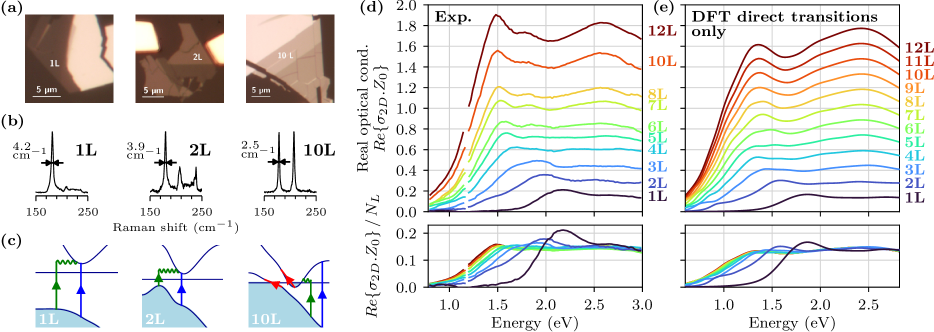
samples are peeled from crystals grown by chemical vapor transport (HQ graphene) using Au-assisted mechanical exfoliation [26, 27], and transferred onto fused silica substrates (Fig. 1a (SM-LABEL:SM-sec:AuAssistExfo). The monolayer to multilayers flakes feature the characteristic Raman signature of the 1T phase [28] (Fig. 1b). The Raman peaks have record narrow linewidths, testifying of the high crystallinity of the exfoliated material. These samples are subjected to a detailed Raman study in reference [29].
III Optical spectroscopy
We use a high-accuracy VIR-vis () micro-absorption setup at room temperature to study the exfoliated flakes (SM-LABEL:SM-sec:microAbsorption). The acquisition of both reflectance and transmittance enables the determination of the complex two-dimensional optical conductivity (SM-LABEL:SM-sec:optConductCalculation). For thin films, its real component (Fig. 1d) is simply the optical absorption in vacuum [30]. We identify the number of layers by using the linear scaling of the real 2D optical conductivity with layer count in the blue end of the electromagnetic spectrum (, Fig. 1d). This attribution is consistent with atomic force microscopy thickness measurements (in combination with Raman spectroscopy, SM-LABEL:SM-sec:AFM). Optical spectra feature a plateau on the blue side, and show a slowly decaying tail on the infrared side. Two dominant peaks can be distinguished (at and for the thick samples), which redshift with increasing thickness. This effect is common in 2D semiconductors [31], but is particularly pronounced in , due to its strong interlayer interaction. The tail decay extends over an energy range – much larger than thermal energy – which cannot be attributed to thermal broadening of the main absorption peak. Interestingly, as the material transits from an indirect semiconductor to semimetal with increasing thickness – within the 3L - 10L range [9, 32, 33, 34, 35, 36] – no semimetallic signature emerges in the infrared end of the absorption spectrum.
IV Optical absorption mechanisms
Several mechanisms can be responsible for the NIR-vis optical absorption: intraband transitions, indirect interband transitions, and direct interband transitions (Fig. 1c) [37].
Owing to the indirect nature of the bandgap, and to the slow decay of the low-energy absorption tail, previous works studying optical absorption conjectured that indirect optical transitions are responsible for infrared absorption [8, 12, 13, 14, 15, 16, 17, 18, 19, 20, 21, 22], and extracted indirect bandgaps using the Tauc model for indirect bandgap semiconductors [38].
In the semimetal , free-electron signatures are in the range [39, 22, 40], and at optical frequencies, the absorption driven by intraband transitions can be neglected compared to the one due to direct transitions. Likewise, in well-down indirect semiconductor silicon and germanium, optical absorption at high energy is dominated by direct transitions, and orders of magnitude smaller indirect transitions are only revealed below the direct optical bandgap [41].
We therefore compare the experimental spectra with the optical absorption deduced from DFT simulation, only considering direct optical transitions (Fig. 1e). DFT computation relies on the GGA-IPA method (SM-LABEL:SM-sec:DFT) for an AA-stacked structure. There is remarkable quantitative agreement between the absorption magnitudes of the simulation and the experiment, and the profile lineshapes feature similar absorption peaks and low-energy absorption tails. This striking correspondence supports that the direct transition mechanism dominates the optical response.
V Band nesting and absorption peaks
We now turn our discussion to the origin of optical absorption specific features, starting with the main absorption peaks. Several works [23, 24, 25] attributed these peaks to bound excitons. By analyzing the simulated optical absorption in detail, we shall see that these peaks originate instead from band nested direct transitions. We focus on the simplest cases of monolayer and bilayer .
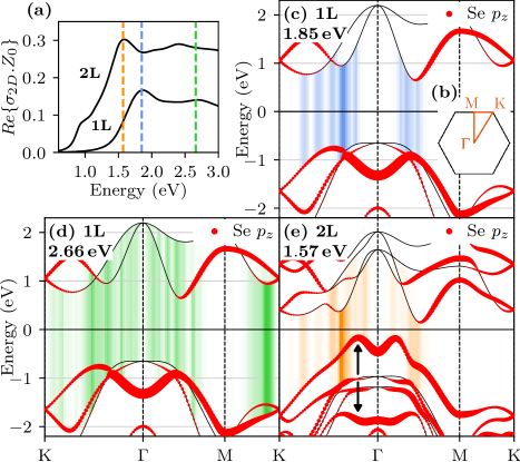
The DFT-computed optical absorption (Fig. 2a) is decomposed on each available direct transition of the band diagram, for a given energy (SM-LABEL:SM-sec:contributionDiagr). The main absorption peaks arise from optical transitions located in the center of the irreducible Brillouin zone (Fig. 2a, b, c, e). For these transitions, the coupled bands are locally parallel, leading to local enhancements in the joint density of state (SM-LABEL:SM-sec:absorptionPeaksJDOS), and consequently in optical absorption peaks – a situation known as the band nesting effect [42]. In a similar fashion, the second absorption peak originates from band nesting in between the M and K points (Fig. 2d). The main absorption peak is mainly arising from optically active transitions from the symmetric selenium orbital to the platinum orbital (SM-LABEL:SM-sec:orbitals). The second peak principally originates from transitions based on the Se and Pt orbitals coupling.
When stacking two monolayers, the interlayer coupling results in a lift of the bands degeneracy. The interlayer hybridization is particularly strong for states composed of an important selenium orbital component (Fig. 2d, e, SM-LABEL:SM-sec:orbitals). Consequently, an upshifted (and downshifted) valence band emerges in the bilayer band diagram (dark arrows Fig. 2e), causing a bandgap reduction. We observe that this upmost valence band is however not involved in the main absorption peak. It instead plays an important role in the low-energy optical absorption.
VI The low-energy absorption tail
The slowly decaying near-infrared absorption tail of has been interpreted as originating from indirect interband absorption. We now provide the experimental evidence that such a mechanism is not involved. Inspecting the computed optical absorption allows to explain the tail profile, only relying on direct optical transitions.
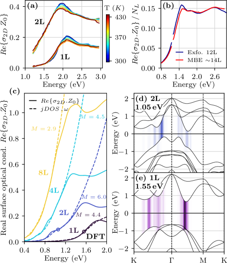
In the case of indirect optical transitions, the momentum mismatch between the two coupled states can be provided either by the phonon bath or by defects in the material. We observe that a -increase does not broaden the absorption tail of the 2L sample, and marginally affects the one of the 1L sample (Fig. 3a, SM-LABEL:SM-sec:thermalDiffRelf), ruling out phonon-assisted indirect transition mechanism. We also compare an exfoliated flake and a thin film grown by molecular beam epitaxy [43]. Both feature different Raman linewidths [29], and should therefore have different types and densities of defects. They however present almost identical absorption tails (Fig. 3b), discarding the hypothesis of a defect-assisted transition mechanism.
Since indirect transitions are experimentally ruled out, we come back to the direct optical transition interpretation guided by the insights provided by DFT. We start by confronting the real 2D optical conductivity with the joint density of states multiplied by frequency (Fig. 3c). They coincide over the absorption tail spectral range, which extends on a large energy range , so that we can write . This form is expected if the involved optical transitions feature a constant light-matter coupling, that we identify here as (SM-LABEL:SM-sec:OptCondDerivation) – suggesting that specific transitions, involving analogous pairs of states, are responsible for the tail absorption. We indeed identify these transitions by inspecting the contributions to optical absorption of 1L and 2L (Fig. 3c and d). They occur between the upmost -based valence band and a conduction band bearing Pt orbital component. For the bilayer sample, a small shoulder appears at which is not as prominent in the (Fig. 3c). It indicates a change in the light-matter coupling , most likely due to the onset of Se to Pt orbital coupling (SM-LABEL:SM-sec:contributionDiagr and LABEL:SM-sec:orbitals). Due to band degeneracy lift when stacking individual layers, the number of optical transitions involved in the absorption tail increases with the layers count (SM Fig. LABEL:SM-fig:absBroadening). Consequently, the monolayer sample exhibits resonant transitions only below its main peak, while the resonant transitions in 2L extend below (Figs 2c, e, SMLABEL:SM-fig:contributions2LTail and 3e). This explains the steeper absorption decrease of 1L (Fig. 1d bottom), which in turn leads to a stronger sensitivity to temperature-induced broadening (Fig. 3a).
VII DFT bandgap correction
While DFT is a tool providing valuable information about the strength and electronic wavefunctions involved in optical transitions, its bandgaps estimates have limited accuracy. We circumvent this problem by using the measured optical absorption to rescale the DFT calculations. In doing so, we determine the indirect bandgap energies and deduce the indirect semiconductor to semimetal transition.
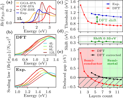
DFT simulations are known to introduce a rigid energy shift of the conduction bands with respect to the valence bands due to misestimation of many-body interactions, leaving the bands profiles essentially unperturbed [44] (SM Fig. LABEL:SM-fig:Bands1LGGAGW). We represent in Fig. 4a the optical absorption of 1L obtained with DFT models beyond GGA-IPA to capture many-body effects. However all the simulations present energy shifts with respect to the experimental results (Fig. 4a), motivating the correction of this shift.
To do so, we choose to use the lowest energy optical signature: the absorption tail. This feature has been previously used to extract bandgaps using Tauc plots. We now rely on the knowledge that this tail results from direct transitions, and derive a scaling law for the bulk limit. Close to the lowest energy direct transition , the energy bands are locally quadratic in momentum and the light-matter coupling can be considered as constant, raising (SM-LABEL:SM-sec:scalingLaw). Applying this law to the DFT-computed and experimental absorption tails, we extract threshold energies by extrapolating the linear slopes to the x-intercept, down to 4L thickness (Fig. 4b and c). Note that as the material is thinned down, 2D electronic confinement leads to the discretization of the z-momentum. Hence the scaling law only applies for thick enough materials (in practice 4L). The inferred threshold values for experimental and simulated data feature a nearly constant energy shift (Fig. 4d). We consequently upshift the DFT indirect bandgap predictions by this value.
With this correction, the transition from indirect semiconductor to semimetallic state occurs around 7 layers, in contrast with initial ab-initio calculations which predicted to be semiconducting up to 2-3 layers [10, 45] (Fig. 4e). Experimental electronic transport and scanning tunneling spectroscopy measurements reported transitions observed between 3 and 10 layers [9, 32, 33, 34, 35, 36]. These estimations present a large spread, which could be explained by the presence of spurious conduction due to defects or the lack of accuracy in the determination of the number of layers. In our work, by employing optical absorption spectroscopy we precisely establish the number of layers, and the use of an indirect method for determining the electronic bandgap makes it insensitive to the presence of defects. A 7-layers semiconductor to semi-metal transition opens the possibility to fine tune the electronic bandgap down to very low values – close to the transition, the bandgap shifts by only – of particular interest for middle and far infrared optoelectronics.
VIII Layer stacking and bound excitons
The optical absorption mechanism demonstrated in our study is supported by robust sample-to-sample reproducibility (SM Fig. LABEL:SM-fig:conductivityRealImagExperimental). Mono and bilayers are however notable exceptions (Fig. 5a, c).
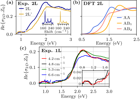
The nature of the interlayer coupling strongly affects 2D materials optical absorption [46], and in particular those of bilayer . The Raman spectral signature allows to sort bilayers in two categories [29], labeled 2L and 2L’ (Fig. 5a). With respect to 2L samples, the 2L’ ones display a blue-shifted main peak, do not have an energy shoulder at , and exhibit a low intensity absorption peak at . These three features are shared with monolayer (Fig. 5c), suggesting that the 2L’ samples have a reduced interlayer coupling. If AA stacking is the most stable configuration of , AB stacking has been predicted to be stable as well [47, 45] and has been found to be a common defect of grown films [43, 48, 49]. Comparing the simulated optical absorption of AA and of two types of AB stacking (Fig. 5b, SM-LABEL:SM-sec:ABStacking), we find that the AB stacked spectra present a characteristic blueshift, and do not have the characteristic shoulder of the AA stacked spectrum. The optical absorption of 2L supports therefore an AA stacked configuration, while the one of 2L’ is likely caused by AB stacking.
We now turn to the monolayers: the sample of worst crystalline quality, featuring a Raman mode linewidth above [29], presents a reduced main peak amplitude with respect to the best samples. This is not surprising as this peak results from band nesting effect, a singularity of the band structure that can particularly be altered by the presence of disorder – even more since it is affected by many-body interactions (GW-BSE in Fig. 4a).
Beyond redistribution of oscillator strength caused by many-body effects, one can wonder if bound excitons might be observed in . We perform a photoluminescence experiment at room temperature within the visible range (SM-LABEL:SM-sec:PL). The measured signal is very weak, and no distinctive excitonic signatures can be identified. Inspecting the optical absorption of monolayer , an unexpected feature is nonetheless observed at lower energy: the high-quality samples, of Raman mode linewidth below , exhibit a absorption peak at (Fig. 5c, SM-LABEL:SM-sec:1LPeak). This peak is located below the absorption tail, in the optical gap, and might well originate from a bound exciton. Future work is needed with high-quality encapsulated samples at low temperature to investigate further its origin.
IX Conclusion
In conclusion, we have shown that the NIR-vis optical absorption – peaks and low-energy tail – of indirect bandgap thin layered arises from single-electron direct optical transitions. As a consequence, we could infer its semiconductor to semimetal transition at 7 layers. This direct and tunable optical absorption paves the way to efficient and ultrafast optoelectronics in the telecom band. Furthermore, the now available high-quality exfoliated down to the monolayer allows to explore many-body effects, such as a potential monolayer exciton at .
X Acknowledgements
We thank Y. Chassagneux and F. Rapisarda for experimental help. The authors acknowledge the financial support from the European Union’s Horizon 2020 program under grant agreement no. 785219, no. 881603 (Core2 and 3 Graphene Flagship) and no. 964735 (FET-OPEN EXTREME-IR), as well as from ANR-2018-CE08-018-05 (BIRDS), ANR-2021-CE24-0025 (ELuSeM), and Thales Systèmes Aéroportés (CIFRE grant No. 2016/1294). This work was granted access to the HPC resources of MesoPSL financed by the Region Ile de France and the project EquipMeso (reference ANR-10-EQPX-29-01) of the program Investissements d’Avenir supervised by the Agence Nationale pour la Recherche.
XI Authors contributions
MT, RLG, CV and EB designed the experiments with the help of PM. MT conducted the sample fabrication with the help of RLG, JP and MR. MT performed the optical spectroscopy measurements and analysis. SA and MA performed the DFT simulations and atomic orbital projection with the help of RF and FC. SA, MA, and MT computed the optical properties. MT computed the atomic orbital couplings. MT and ED performed the Raman spectroscopy. ED and PL grew the MBE thin film. MT, SA, RLG, BP, FC, CV, RF and EB developed the theoretical interpretation. MT and EB wrote the manuscript with contributions from the coauthors.
XII Data availability
Data are publicly available at 10.5281/zenodo.10138281.
References
- Schmidt et al. [2015] H. Schmidt, F. Giustiniano, and G. Eda, Chemical Society Reviews 44, 7715 (2015).
- Mak and Shan [2016] K. F. Mak and J. Shan, Nature Photonics 10, 216 (2016).
- Wang et al. [2022] Y. Wang, L. Zhou, M. Zhong, Y. Liu, S. Xiao, and J. He, Nano Research 15, 3675 (2022).
- Goff et al. [2021] R. L. Goff, M. Rosticher, Y. Peng, Z. Liu, T. Taniguchi, K. Watanabe, J.-M. Berroir, E. Bocquillon, G. Fève, C. Voisin, J. Chazelas, B. Plaçais, and E. Baudin, 2D Materials 8, 035035 (2021).
- Wang et al. [2015] Y. Wang, L. Li, W. Yao, S. Song, J. T. Sun, J. Pan, X. Ren, C. Li, E. Okunishi, Y.-Q. Wang, E. Wang, Y. Shao, et al., Nano Letters 15, 4013 (2015).
- Wang et al. [2021] G. Wang, Z. Wang, N. McEvoy, P. Fan, and W. J. Blau, Advanced Materials 33, 2004070 (2021).
- Bonell et al. [2021] F. Bonell, A. Marty, C. Vergnaud, V. Consonni, H. Okuno, A. Ouerghi, H. Boukari, and M. Jamet, 2D Materials 9, 015015 (2021).
- Zhao et al. [2017] Y. Zhao, J. Qiao, Z. Yu, P. Yu, K. Xu, S. P. Lau, W. Zhou, Z. Liu, X. Wang, W. Ji, and Y. Chai, Advanced Materials 29, 1604230 (2017).
- Ciarrocchi et al. [2018] A. Ciarrocchi, A. Avsar, D. Ovchinnikov, and A. Kis, Nature Communications 9, 919 (2018).
- Villaos et al. [2019] R. A. B. Villaos, C. P. Crisostomo, Z.-Q. Huang, S.-M. Huang, A. A. B. Padama, M. A. Albao, H. Lin, and F.-C. Chuang, npj 2D Materials and Applications 3, 2 (2019).
- Wang et al. [2005] F. Wang, G. Dukovic, L. E. Brus, and T. F. Heinz, Science 308, 838 (2005).
- Xie et al. [2019] J. Xie, D. Zhang, X.-Q. Yan, M. Ren, X. Zhao, F. Liu, R. Sun, X. Li, Z. Li, S. Chen, Z.-B. Liu, and J.-G. Tian, 2D Materials 6, 035011 (2019).
- Chen et al. [2019] X. Chen, S. Zhang, L. Wang, Y.-F. Huang, H. Liu, J. Huang, N. Dong, W. Liu, I. M. Kislyakov, J. M. Nunzi, L. Zhang, and J. Wang, Photon. Res. 7, 1416 (2019).
- Shi et al. [2019] J. Shi, Y. Huan, M. Hong, R. Xu, P. Yang, Z. Zhang, X. Zou, and Y. Zhang, ACS Nano 13, 8442 (2019).
- Zhao et al. [2019] X. Zhao, F. Liu, D. Liu, X.-Q. Yan, C. Huo, W. Hui, J. Xie, Q. Ye, C. Guo, Y. Yao, Z.-B. Liu, and J.-G. Tian, Applied Physics Letters 115, 263102 (2019).
- Wang et al. [2019] L. Wang, S. Zhang, N. McEvoy, Y.-y. Sun, J. Huang, Y. Xie, N. Dong, X. Zhang, I. M. Kislyakov, J.-M. Nunzi, L. Zhang, and J. Wang, Laser & Photonics Reviews 13, 1900052 (2019).
- Gulo et al. [2020] D. P. Gulo, H. Yeh, W.-H. Chang, and H.-L. Liu, Scientific Reports 10, 19003 (2020).
- Fu et al. [2020] J. Fu, W. Xu, X. Chen, S. Zhang, W. Zhang, P. Suo, X. Lin, J. Wang, Z. Jin, W. Liu, and G. Ma, The Journal of Physical Chemistry C 124, 10719 (2020).
- Ermolaev et al. [2021] G. A. Ermolaev, K. V. Voronin, M. K. Tatmyshevskiy, A. B. Mazitov, A. S. Slavich, D. I. Yakubovsky, A. P. Tselin, M. S. Mironov, R. I. Romanov, A. M. Markeev, I. A. Kruglov, S. M. Novikov, A. A. Vyshnevyy, A. V. Arsenin, and V. S. Volkov, Nanomaterials 11, 3269 (2021).
- Chung et al. [2021] C.-C. Chung, H. Yeh, P.-H. Wu, C.-C. Lin, C.-S. Li, T.-T. Yeh, Y. Chou, C.-Y. Wei, C.-Y. Wen, Y.-C. Chou, C.-W. Luo, C.-I. Wu, M.-Y. Li, L.-J. Li, W.-H. Chang, and C.-W. Chen, ACS Nano 15, 4627 (2021).
- Zheng et al. [2022] Z. Zheng, Z. Peng, Z. Yu, H. Lan, S. Wang, M. Zhang, L. Li, H. Liang, and H. Su, Results in Physics 42, 106012 (2022).
- Su et al. [2023] H. Su, Z. Zheng, Z. Yu, S. Feng, H. Lan, S. Wang, M. Zhang, L. Li, and H. Liang, Nanomaterials 13, 795 (2023).
- He et al. [2020] J. He, W. Jiang, X. Zhu, R. Zhang, J. Wang, M. Zhu, S. Wang, Y. Zheng, and L. Chen, Phys. Chem. Chem. Phys. 22, 26383 (2020).
- He et al. [2022] J. He, X. Zhu, W. Liu, E. Hu, J. Wang, and R. Zhang, Nano Research 15, 6613 (2022).
- Bae et al. [2021] S. Bae, S. Nah, D. Lee, M. Sajjad, N. Singh, K. M. Kang, S. Kim, G.-J. Kim, J. Kim, H. Baik, K. Lee, and S. Sim, Small 17, 2103400 (2021).
- Desai et al. [2016] S. B. Desai, S. R. Madhvapathy, M. Amani, D. Kiriya, M. Hettick, M. Tosun, Y. Zhou, M. Dubey, J. W. Ager III, D. Chrzan, and A. Javey, Advanced Materials 28, 4053 (2016).
- Heyl et al. [2020] M. Heyl, D. Burmeister, T. Schultz, S. Pallasch, G. Ligorio, N. Koch, and E. J. W. List-Kratochvil, physica status solidi (RRL) – Rapid Research Letters 14, 2000408 (2020).
- O’Brien et al. [2016] M. O’Brien, N. McEvoy, C. Motta, J.-Y. Zheng, N. C. Berner, J. Kotakoski, K. Elibol, T. J. Pennycook, J. C. Meyer, C. Yim, M. Abid, T. Hallam, J. F. Donegan, S. Sanvito, and G. S. Duesberg, 2D Materials 3, 021004 (2016).
- Tharrault et al. [2023] M. Tharrault, E. Desgué, D. Carisetti, B. Plaçais, C. Voisin, P. Legagneux, and E. Baudin, Raman spectroscopy of monolayer to bulk ptse2 exfoliated crystals (2023), arXiv:2307.15520 [cond-mat.mtrl-sci] .
- Li and Heinz [2018] Y. Li and T. F. Heinz, 2D Materials 5, 025021 (2018).
- Zhao et al. [2013] W. Zhao, Z. Ghorannevis, L. Chu, M. Toh, C. Kloc, P.-H. Tan, and G. Eda, ACS Nano 7, 791 (2013).
- Yim et al. [2018] C. Yim, V. Passi, M. C. Lemme, G. S. Duesberg, C. Ó Coileáin, E. Pallecchi, D. Fadil, and N. McEvoy, npj 2D Materials and Applications 2, 5 (2018).
- Ansari et al. [2019] L. Ansari, S. Monaghan, N. McEvoy, C. Ó. Coileáin, C. P. Cullen, J. Lin, R. Siris, T. Stimpel-Lindner, K. F. Burke, G. Mirabelli, R. Duffy, E. Caruso, R. E. Nagle, G. S. Duesberg, P. K. Hurley, and F. Gity, npj 2D Materials and Applications 3, 33 (2019).
- Das et al. [2021] T. Das, E. Yang, J. E. Seo, J. H. Kim, E. Park, M. Kim, D. Seo, J. Y. Kwak, and J. Chang, ACS Applied Materials & Interfaces 13, 1861 (2021).
- Zhang et al. [2021] L. Zhang, T. Yang, M. F. Sahdan, Arramel, W. Xu, K. Xing, Y. P. Feng, W. Zhang, Z. Wang, and A. T. S. Wee, Advanced Electronic Materials 7, 2100559 (2021).
- Li et al. [2021] J. Li, S. Kolekar, M. Ghorbani-Asl, T. Lehnert, J. Biskupek, U. Kaiser, A. V. Krasheninnikov, and M. Batzill, ACS Nano 15, 13249 (2021).
- Yu and Cardona [2010] P. Y. Yu and M. Cardona, Optical properties, in Fundamentals of Semiconductors: Physics and Materials Properties (Springer Berlin Heidelberg, Berlin, Heidelberg, 2010).
- Viezbicke et al. [2015] B. D. Viezbicke, S. Patel, B. E. Davis, and D. P. Birnie III, physica status solidi (b) 252, 1700 (2015).
- Ji et al. [2023] J. Ji, Y. Zhou, B. Zhou, E. Desgué, P. Legagneux, P. U. Jepsen, and P. Bøggild, ACS Applied Materials & Interfaces 10.1021/acsami.3c09792 (2023).
- Hemmat et al. [2023] M. Hemmat, S. Ayari, S. Dhillon, et al., Article in preparation (2023).
- Dash and Newman [1955] W. C. Dash and R. Newman, Phys. Rev. 99, 1151 (1955).
- Carvalho et al. [2013] A. Carvalho, R. M. Ribeiro, and A. H. Castro Neto, Phys. Rev. B 88, 115205 (2013).
- Desgué et al. [2023] E. Desgué, P. Legagneux, et al., Article in preparation (2023).
- Hüser et al. [2013] F. Hüser, T. Olsen, and K. S. Thygesen, Phys. Rev. B 87, 235132 (2013).
- Kandemir et al. [2018] A. Kandemir, B. Akbali, Z. Kahraman, S. V. Badalov, M. Ozcan, F. Iyikanat, and H. Sahin, Semiconductor Science and Technology 33, 085002 (2018).
- Liang et al. [2022] J. Liang, D. Yang, J. Wu, J. I. Dadap, K. Watanabe, T. Taniguchi, and Z. Ye, Phys. Rev. X 12, 041005 (2022).
- Fang et al. [2019] L. Fang, W. Liang, Q. Feng, and S.-N. Luo, Journal of Physics: Condensed Matter 31, 455001 (2019).
- Xu et al. [2021] L. Xu, H. Liu, C. Song, X. Li, F. Li, D. Li, L. Wang, X. Bai, and J. Qi, 2D Materials 8, 025014 (2021).
- Ryu et al. [2019] G. H. Ryu, J. Chen, Y. Wen, and J. H. Warner, Chemistry of Materials 31, 9895 (2019).