Cryogenic spin Peltier effect detected by a RuO2-AlOx on-chip microthermometer
Abstract
We report electric detection of the spin Peltier effect (SPE) in a bilayer consisting of a Pt film and a Y3Fe5O12 (YIG) single crystal at the cryogenic temperature as low as 2 K based on a RuO2AlOx on-chip thermometer film. By means of a reactive co-sputtering technique, we successfully fabricated RuO2AlOx films having a large temperature coefficient of resistance (TCR) of at around . By using the RuO2AlOx film as an on-chip temperature sensor for a Pt/YIG device, we observe a SPE-induced temperature change on the order of sub-, the sign of which is reversed with respect to the external magnetic field direction. We found that the SPE signal gradually decreases and converges to zero by increasing up to . The result is attributed to the suppression of magnon excitations due to the Zeeman-gap opening in the magnon dispersion of YIG, whose energy much exceeds the thermal energy at 2 K.
I INTRODUCTION
One of the important features in spintronics is that various phenomena have been found at room temperature in simple stacked structures, leading to their practical device applications Ohno2016ProcIEEE ; Chumak2022IEEETransMagn ; Yang2022Nature ; Maekawa2023JAP . Meanwhile, exploring the spintronic phenomena at low temperatures often resulted in a discovery of new functional properties with both fundamental and practical prospects Fan2014NatMat ; Linder2015NatPhys ; Umeda2018APL ; Yao2018PRB ; Shiomi2019NatPhys ; Jeon2020ACSNano ; Tschirhart2023NatPhys . A typical example is the spin Seebeck effect (SSE), which refers to the generation of a spin current as a result of a temperature gradient in a magnetic material, and has been observed at room temperature in a variety of magnetic materials, including garnet- and spinel-ferrites with high magnetic ordering temperaturesUchida2016ProcIEEE ; Rezende_text ; Kikkawa2023ARCMP . When SSEs are measured at low temperatures in certain systems however, intriguing physics comes to the surface. Major findings include the signal anomalies induced by hybridized magnon-phonon excitationsKikkawa2023ARCMP ; Kikkawa2016PRL ; Cornelissen2017PRB ; Oyanagi2020AIPAdv ; Li2020PRL_Cr2O3 ; Kikkawa2022PRMater , unconventional sign reversal due to competing magnon modes having opposite spin polarizationsGeprags2016NatCommun , observation of a spin-superfluid-mediated nonlocal SSE signalYuan2018SciAdv , and SSEs driven by paramagnetic spinsWu2015PRL ; Oyanagi2023PRB and exotic elementary excitations in quantum spin systemsHirobe2017NatPhys ; Chen2021NatCommun ; Xing2022APL . Furthermore, recently, a nuclear SSE has been observed in an antiferromagnet having strong hyperfine couplingKikkawa2021NatCommun ; Kikkawa2023ARCMP . The signal increases down to ultralow temperatures on the order of , which is distinct from conventional thermoelectric effects in electronic (spin) systemsKikkawa2023ARCMP ; Kikkawa2021NatCommun , and may offer an opportunity for exploring thermoelectric science and technologies at ultralow temperatures, an important environment in quantum information science.
In contrast to the intense research on SSEs, the spin Peltier effect Flipse2014PRL ; Daimon2016NatCommun ; Daimon2017PRB ; Itoh2017PRB ; Yagmur2018JPhysD ; Sola2019SciRep ; Yahiro2020PRB ; Yamazaki2020PRB ; Daimon2020APEX ; Uchida2021Review ; Uchida2021JPSJ ; Takahagi2023APL , the reciprocal of the SSE, remains to be explored at low temperatures below 100 K because of its experimental difficulty. The SPE modulates the temperature of a junction consisting of a metallic film and a magnet in response to a spin currentDaimon2016NatCommun , and has been detected usually by means of lock-in thermography (LIT) Daimon2016NatCommun ; Daimon2017PRB ; Yagmur2018JPhysD ; Daimon2020APEX and thermocouples Flipse2014PRL ; Itoh2017PRB ; Yahiro2020PRB . The LIT measures the infrared intensity emitted from the sample surface based on a combination of the lock-in with temperature imaging technique, whose intensity is in proportion to the fourth power of the absolute temperature (the Stefan–Boltzmann lawYagmur2018JPhysD ; Uchida2021JPSJ ). This results in a typical resolution of 0.1 mK at room temperature Uchida2021JPSJ , which is sufficient to measure a SPE in a prototypical Pt/Y3Fe5O12 (YIG) system at higher temperatures ( room temperature and above) Daimon2016NatCommun ; Daimon2017PRB . However, the LIT may not be applicable for detecting the low-temperature SPE, because its sensitivity is dramatically reduced with decreasing temperature Yagmur2018JPhysD ; Uchida2021JPSJ . Furthermore, a thermocouple micro-sensor with a high resolution of was used to measure a SPE down to 100 K in Ref. Yahiro2020PRB, . However, it was found to be difficult to conduct the measurements below 100 K as the sensitivity of the thermocouple decreases with decreasing . It is therefore important to establish an alternative experimental method for detecting cryogenic SPEsMaekawa2023JAP . An ultimate goal in this direction would be to find cryogenic SPEs driven by nuclear and quantum spins that can be activated even at ultralow temperatures, toward future possible cooling- and heat-pump technologies in such an environment.
In this study, we have explored the SPE at a cryogenic temperature below the liquid-4He temperature in a prototypical Pt/YIG system. There are three crucial requirements for practical realization of such measurement that are (1) the high temperature-resolution of sub--order or better at low temperatures, (2) ability to detect a temperature change of a metallic (Pt) thin film (which implies for contact-mode measurements sufficient thermal coupling and low heat capacity), and (3) reliability under a high magnetic-field environment. To realize the thermometry that meets these requirements, we adopted a RuO2-based micro-thermometer Pobell-textbook ; LakeShore ; Bosch1986Cryogenics ; Li1986Cryogenics ; Batko1995Cryogenics ; Neppert1996Cryogenics ; Affronte1997JLowTempPhys ; Chen2003 ; Chen2009 ; Nelson2015RevSciInstrum (RuO2AlOx composite film in our case). In general, RuO2-based resistors show a high temperature-sensitivity due to their large negative temperature coefficient of resistance. Besides, they show reasonably small magnetoresistance and can be made in a thin-film form. Owing to these advantages, in fact, RuO2-based chip resistors have widely been used as temperature sensors at cryogenic temperatures Pobell-textbook ; LakeShore . We have fabricated RuO2AlOx films by means of a co-sputtering technique and found the optimal fabrication condition by characterizing their electric transport properties. By using a RuO2AlOx film as an on-chip temperature sensor for a Pt-film/YIG-slab system, we successfully measured a SPE-induced temperature change on the order of sub- at . Our results provide an important step toward a complete physical picture of the SPE and establishment of cryogenic spin(calori)tronics Uchida2021Review .
II EXPERIMENTAL PROCEDURE
II.1 Fabrication of RuO2AlOx films
We have fabricated RuO2AlOx composite films as a micro-thermometer by means of d.c. co-sputtering technique from RuO2 (99.9%, 2-inch diameter) and Al (99.999%, 2-inch diameter) targets under Ar and O2 atmosphere. To obtain the most suitable thermometer film for the SPE at low temperatures, a series of co-sputtered RuO2AlOx films on thermally-oxidized Si substrates was first prepared at several d.c. power values for the RuO2 target (, , , , and ) and the fixed d.c. power for the Al target () under a sputtering gas of Ar + 7.83 vol.% O2 at a pressure of 0.13 Pa at room temperature. Here, the values of ArO2 gas amount and the d.c. power of were chosen such that highly-insulating AlOx films are obtained with a reasonable deposition rate () when AlOx is sputtered solely from the Al target. We note that, if the O2 gas amount exceeds an onset value, the d.c. sputtering rate suddenly decreases due to the surface oxidization of the Al target Maniv1980AlOx ; Wallin2008AlOx , whereas if the O2 gas amount is insufficient, the resultant AlOx film may show finite electrical conduction. We found that the introduction of O2 by itself does not play an important role in the temperature variation of the resistance for pure RuO2 films (for details, see APPENDIX A). To keep the sputtering conditions and resultant films’ quality as consistent as possible through repeated deposition cycles, we introduced common pre-sputtering processes just before actual depositions. To remove a possible oxidized top layer of the Al target, it was pre-sputtered at a relatively high power of for 600 s without introducing O2 gas, and then the RuO2 and Al targets were pre-sputtered for 60 s under the actual deposition conditions (i.e., Ar + 7.83 vol.% O2) Comment_maintenance . For electric transport measurements of the RuO2AlOx films, they were patterned into a Hall-bar shape having the length, width, and thickness of , , and , respectively, by co-sputtering RuO2AlOx through a metal mask. The RuO2 content in the RuO2AlOx films under the different RuO2 sputtering power was evaluated through scanning electron microscopy with energy dispersive X-ray analysis (SEM-EDX) and the surface roughness of the films was characterized through atomic force microscopy (AFM).
II.2 Fabrication of SPE device
To investigate the SPE below the liquid-4He temperature, we have prepared devices consisting of a Pt-film/YIG-slab bilayer, where a 100-nm-thick RuO2AlOx film with Au/Ti electrodes is attached on the top surface of the Pt film to detect its SPE-induced temperature change [see the schematic illustrations and the optical microscope image of a typical SPE device shown in Figs. 1(a) – 1(c)]. Three photolithography steps were employed to make the SPE devices, where all the film depositions were performed at room temperature. First, a 5-nm-thick Pt wire with the width of was formed on the (111) surface of a single-crystalline YIG slab with the size of by d.c. magnetron sputtering in a Ar atmosphere under the d.c. power of 20 W. In the next photolithography step, a 70-nm-thick insulating AlOx layer was formed at the area of [ for the device shown in Fig. 1(c)] on top of the Pt/YIG layer to electrically isolate the RuO2AlOx film from the Pt layer. Here, the AlOx deposition was done by r.f. magnetron sputtering from an Al2O3 target (99.99%, 2-inch diameter) under the r.f. power of 150 W and a sputtering gas of Ar + 1.0 vol.% O2 Voigt2004AlOx at a pressure of 0.6 Pa. We later confirmed that the AlOx film shows a high electric resistance on the order of along the out-of-plane direction at room temperature. Subsequently, a 100-nm-thick RuO2AlOx thermometer film was deposited on top of the AlOx layer at the area of [ for the device shown in Fig. 1(c)] through the co-sputtering under the d.c. sputtering power of and . Here, the dimensions and sputtering power for the RuO2AlOx film were chosen such that the resistance of the resulting film is several tens of k at 2 K and its sensitivity monotonically increases with decreasing down to Comment_different-T [as shown in Figs. 3 and 4(d) and discussed in Sec. III.1].
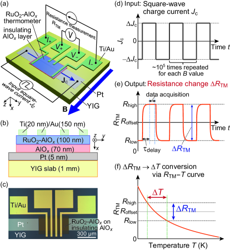
We then proceeded with the final photolithography step for Au(150 nm)/Ti(20 nm) electrodes, where the numbers in parentheses represent the thicknesses of the deposited films. Each Au/Ti electrode wire on the RuO2AlOx film has the - width and is placed at - intervals. To reduce the contact resistance between the RuO2AlOx and Ti films, Ar-ion milling was performed directly before depositing the Au/Ti film. Both the Ti and Au layers were formed by r.f. magnetron sputtering in succession without breaking vacuum. The first lithography process for the Pt layer was done using a single-layer photoresist (AZ5214E) followed by a lift-off process, whereas the second and third processes for the AlOx/RuO2AlOx and Au/Ti layers were done using a double-layered photoresist (LOR-3A and AZ5214E) to provide an undercut structure for a better success rate of the lift off process.
II.3 SPE and SSE measurements
Figure 1(a) shows a schematic illustration of the SPE device and the experimental setup in the present study. The SPE appears as a result of the interfacial spin and energy transfer between magnons in YIG and electron spins in Pt Flipse2014PRL ; Daimon2016NatCommun ; Daimon2017PRB ; Itoh2017PRB . Suppose that the magnetization of the YIG layer is oriented along the direction by the external magnetic field , as shown in Fig. 1(a). With the application of a charge current to the Pt film, the spin Hall effect (SHE)SHE_Hoffman ; SHE_Sinova induces a nonequilibrium spin, or magnetic moment, accumulation at the Pt/YIG interface Flipse2014PRL ; Daimon2016NatCommun ; Daimon2017PRB ; Itoh2017PRB ; Yahiro2020PRB . For (), the accumulated magnetic moment at the interfacial Pt orients along the () direction Schreier2014JPhysD ; Daimon2017PRB , which is antiparallel (parallel) to the direction in Fig. 1(a). Through the interfacial spin-flip scattering, creates or annihilates a magnon in YIG; the number of magnons in YIG increases (decreases) when ()Uchida2021Review ; Maekawa2023JAP . Because of energy conservation, this process is accompanied by a heat flow between the electron in Pt and the magnon in YIGUchida2021Review ; Maekawa2023JAP . The temperature of Pt (YIG) thus decreases (increases) when under and [Fig. 1(a)], whereas the temperature of Pt (YIG) increases (decreases) when by reversing either or in Fig. 1(a)Daimon2016NatCommun ; Daimon2017PRB ; Itoh2017PRB ; Yahiro2020PRB . The SPE-induced temperature change satisfies the following relationship Daimon2016NatCommun ; Daimon2017PRB ; Itoh2017PRB
| (1) |
For the electric SPE detection based on the on-chip thermometer (TM), we utilized the highly-accurate resistance measurement scheme called the Delta mode, a combination of low-noise current source and nanovoltmeter (Keithley Model 6221 and 2182A Itoh2017PRB ; Yahiro2020PRB ). We applied a square-wave charge current with amplitude to the Pt film [Figs. 1(a) and 1(d)] and measured the 4 terminal RuO2AlOx resistance that responds to the change in the polarity, , where () represents the value for and was measured under the sensing current of applied to the RuO2AlOx film [see Figs. 1(a) and 1(e)] Itoh2017PRB . Here, the value is free from the Joule-heating-induced resistance change () that is independent of time, which thereby only contributes to the offset resistance of the RuO2AlOx film shown in Fig. 1(e) Comment_Joule-heating . During the SPE measurement, the magnetic field (with magnitude ) was applied in the film plane and perpendicular to the Pt wire, i.e., in Fig. 1(a), except for the control experiment shown in Fig. 4(b), where . The resistance was recorded after the time delay of [except for the dependence shown in Fig. 4(e)] during the data acquisition time of Comment_frequency , and then was accumulated by repeating the process of the -polarity change times for each point [see Fig. 1(d)] to improve the signal-to-noise ratio. can be converted into the corresponding temperature change by using the sensitivity of the RuO2AlOx film [see Figs. 1(f) and 4(d)].
To compare the dependence of the SPE signal with that of the SSE, we also measured the SSE at using the same device, for which all SPE results presented in this paper were obtained, but in a different experimental run from the SPE measurement. Here, the SSE measurement was done by means of a lock-in detection technique Wu2015PRL ; Kikkawa2022PRMater ; Kikkawa2021NatCommun and the RuO2AlOx layer was used as a resistive heater; an a.c. charge current with the amplitude of and the frequency of was applied to the RuO2-AlOx film, and the second harmonic voltage in the Pt layer induced by a spin current (driven by a heat current due to the Joule heating of the RuO2-AlOx film ) was detected. During the SSE measurement, the external field was applied in the film plane and perpendicular to the Pt wire, i.e., in Fig. 1(a).
III RESULTS AND DISCUSSION
III.1 Electrical conduction in RuO2AlOx films
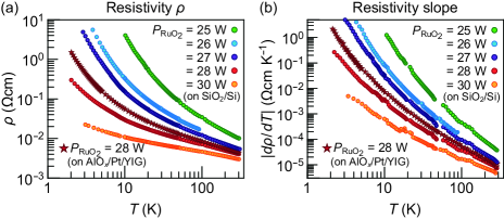
We first characterize the electrical conduction of the RuO2AlOx films on thermally-oxidized Si substrates. Figure 2(a) shows the dependence of the resistivity for the films grown under the several (fixed) sputtering power values for the RuO2 (Al) target (). For all the films, increases with decreasing in the entire temperature range, showing a negative temperature coefficient of resistance (TCR). Both and its slope increase significantly at low temperatures and monotonically by decreasing the RuO2 sputtering power . The overall – curve shifts toward the upper right by decreasing . The result shows that the versus characteristics of the RuO2AlOx films can be controlled simply by changing the sputtering power . SEM-EDX analysis reveals that the RuO2/AlOx ratio decreases by decreasing [Fig. 2(c)], which leads to the increase in the electric transport. We also characterized the RuO2AlOx films by means of AFM and found that a typical root-mean-squared surface roughness is , much smaller than their thickness [see the AFM image of the RuO2AlOx films grown under and (the RuO2 content of 41%) shown in Fig. 2(d)].
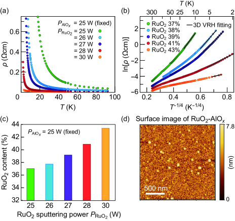
The electrical conduction at sufficiently low temperatures for RuO2-based thermometers has often been analyzed by the variable-range hopping (VRH) model for three dimensional (3D) systems proposed by Mott Pobell-textbook ; Mott1969PhilosMag ; Ambegaokar1971PRB ; Bosch1986Cryogenics ; Li1986Cryogenics ; Batko1995Cryogenics ; Neppert1996Cryogenics ; Affronte1997JLowTempPhys ,
| (2) |
where is the resistivity coefficient and is the characteristic temperature related to the electron localization length . To discuss our result in light of the VRH, we plot versus for the RuO2AlOx films in Fig. 2(b). We found that scales linearly with at low- ranges, and the – data is well fitted by Eq. (2) [see the black solid lines in Fig. 2(b)], suggesting that the low- electrical conduction is indeed governed by the VRH. From the fitting, the values are obtained as , , , , and for the RuO2AlOx films grown under , , , , and , respectively. We note that, at all the ranges adopted for the VRH fitting, the average hopping distance () is larger than the electron localization length () that is the requirement for the VRH model to be valid: Rosenbaum1991PRB ; Lafuerza2013PRB ; Lu2014APL ; Chen2021JPhysD ; Li2022JMaterSci . Besides, the Mott hopping energy (: the Boltzmann constant) obtained for the present films is larger than (or comparable to) the thermal energy , allowing for the electron hopping Rosenbaum1991PRB ; Lafuerza2013PRB ; Lu2014APL ; Chen2021JPhysD ; Li2022JMaterSci . The above argument further confirms the validity of the 3D Mott VRH model to describe the conduction mechanism in the RuO2AlOx films.
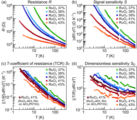
We here discuss the -dependent thermometer characteristics of the RuO2AlOx films. Figure 3 shows the dependence of (a) the resistance , (b) the sensitivity , (c) the temperature coefficient of resistance (TCR) , and (d) the dimensionless sensitivity for the RuO2AlOx films. Here, the sensitivity is an essential quantity when the thermometer is used as an actual temperature-sensor device in its original form. The TCR is the normalized sensitivity by the measured resistance , given that is geometry dependent (i.e., scales with ) LakeShore . The dimensionless sensitivity is a measure often used to compare the performance of the thermometers made of different materials, regardless of their size Harris2021RevSciInstrum ; Scott2022JAP ; LakeShore ; Courts2003AIPConfProc . For the present RuO2AlOx films with low RuO2 content (), the sensitivity takes a high value on the order of below . For such a low- range, however, their resistance values are highly enhanced, and exceed at , which is too high to use such films as thermometers in their original dimensions below the liquid-4He temperature. Besides, their TCR values start to show a saturation behavior by decreasing in such a low- environment. By contrast, the RuO2AlOx film with the RuO2 content of 41% (fabricated under and ) shows a moderate () value of () and the best TCR characteristic of around . We therefore adopt its growth condition for our SPE device. Overall, the , TCR, and values of the present RuO2AlOx films are comparable to those of commercially available Cernox™ zirconium oxy-nitride sensors LakeShore ; Courts2003AIPConfProc , carbon composites Clement1952RevSciInstrum ; Lawless1972RevSciInstrum ; Pobell-textbook , and AuGe films Scott2022JAP commonly used at a similar range.
III.2 Observation of SPE based on RuO2AlOx on-chip thermometer
We are now in a position to demonstrate a cryogenic SPE in the Pt/YIG sample based on the RuO2AlOx on-chip thermometer. Figure 4(a) shows the dependence of the RuO2AlOx resistance change measured at and a low- range of . With the application of the charge current to the Pt film, a clear signal appears with a magnitude saturated at Comment_undulation and its sign changes depending on the direction. The signal disappears either when is essentially zero [gray diamonds in Fig. 4(a)] or when is applied perpendicular to the Pt/YIG interface () [Fig. 4(b)]. We also confirmed that the dependence of is consistent with that of the SSE in the identical Pt/YIG device [see Fig. 4(c)]. These are the representative features of the SPE Daimon2016NatCommun ; Daimon2017PRB ; Itoh2017PRB ; Yagmur2018JPhysD ; Sola2019SciRep ; Yahiro2020PRB ; Yamazaki2020PRB ; Daimon2020APEX ; Uchida2021Review ; Uchida2021JPSJ . Furthermore, the sign of agrees with the SPE-induced temperature changeDaimon2016NatCommun ; Daimon2017PRB . As shown in Fig. 4(a), the measured value is positive for , meaning that the resistance increases (decreases) when (), for which the orientation of the SHE-induced magnetic moment at the interfacial Pt layer is () in Fig. 1(a). According to the negative TCR of the RuO2AlOx film, this implies that the temperature of the Pt film decreases (increases) when () under . This correspondence between the sign of the temperature change and the relative orientation of with respect to is consistent with the scenario of the SPE described in Sec. II.3. We thus conclude that we succeeded in measuring a cryogenic SPE using the RuO2AlOx on-chip thermometer film.
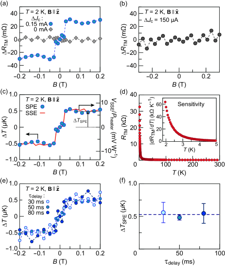
To convert the value to the temperature change , we measured the – curve for the RuO2AlOx film. As shown in Fig. 4(d), similar to the results described in Sec. III.1, its resistance increases dramatically with decreasing at low temperatures, and the sensitivity is as large as at 2 K [The TCR and dimensionless sensitivity for the film are plotted in Figs. 3(c) and 3(d), respectively, and and are plotted in Figs. 7(a) and 7(b) in APPENDIX B, respectively, together with the results for the RuO2AlOx films grown on thermally-oxidized Si substrates]. In Fig. 4(c), we replot the dependence of the SPE in units of the temperature change using the above value. We evaluate the magnitude of the SPE-induced temperature change to be , by averaging the values for , at which the magnetization of the YIG slab fully orients along the directionUchida2015PRB [see the dashed line in Fig. 4(c)]. The standard deviation of shows that our measurement scheme based on the RuO2AlOx on-chip thermometer can resolve an extremely small on the order of several tens of nK (which is a value achieved by repeating the process of the -polarity change of times at each ). The resolution is much higher than that reported in the previous SPE measurements based on lock-in thermography, lock-in thermoreflectance, and thermocouples, for which the typical resolution is , , and , respectivelyYahiro2020PRB ; Uchida2021JPSJ ; Takahagi2023APL . We found that the magnitude of normalized by the charge-current density applied to the Pt wire is , which is two orders of magnitude smaller than the corresponding value for Pt/YIG systems measured at room temperature Daimon2017PRB ; Itoh2017PRB . The low- signal reduction of the SPE is consistent with that found in the SSE Kikkawa2015PRB ; Jin2015PRB ; Kikkawa2016JPSJ ; Oyanagi2020AIPAdv , and is attributed mainly to the reduction of the thermally activated magnons contributing to these phenomena at cryogenic temperatures. Besides, there can be a finite temperature gradient across the insulating AlOx film, between the Pt and RuO2AlOx layers, resulting in further decrease of the detected signal. We also measured the delay time dependence of the SPE and found that the takes almost the same value in the present range () [see Figs. 4(e) and 4(f)], showing that all the data were obtained under the steady-state condition Itoh2017PRB ; Yamazaki2020PRB .
We also explored the high magnetic field response of the SPE signal. Figure 5(a) displays the versus data measured at and (). We found that exhibits a maximum at a low () and, by increasing , gradually decreases and is eventually suppressed. The dependence of the SPE agrees well with that of the SSE measured with the identical device [see Fig. 5(a)]. We note that the magnetoresistance (MR) ratio of the RuO2AlOx film is as small as for at , so that the device can be used reliably under the high- range. The observed feature is explained in terms of the suppression of magnon excitations by the Zeeman effect, as established in the previous SSE research Kikkawa2015PRB ; Jin2015PRB ; Kikkawa2016JPSJ ; Oyanagi2020AIPAdv ; Kikkawa2021NatCommun [see Fig. 5(b)]. By increasing , the magnon dispersion shifts toward high frequencies due to the Zeeman interaction (). At , the Zeeman energy is in units of temperature, which is greater than the thermal energy at 2 K [see Fig. 5(b)], resulting in an insignificant value of the Boltzmann factor: , where and represent the gyromagnetic ratio and Dirac constant, respectively. Therefore, the thermal magnons that can contribute to the SPE at a low are gradually suppressed with the increase of and, at , are hardly excited by the strong Zeeman gap in the magnon spectrum [Fig. 5(b)], which leads to the suppression of the SPE in the low- and high- environment.
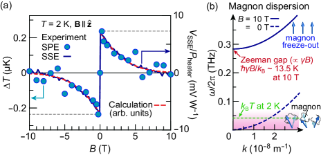
We also compared the experimental result with a calculation for the interfacial heat current induced by the SPE and spin current induced by the SSE , which are expressed as
| (3) |
respectively Kikkawa2015PRB ; Adachi2013review ; Bender2015PRB ; Cornelissen2016PRB ; Ohnuma2017PRB . Here, is the parabolic magnon dispersion for YIG with the stiffness constant of Kikkawa2016PRL and is the BoseEinstein distribution function. Note that the relation ensures the Onsager reciprocity between the SSE and SPEOhnuma2017PRB , which makes the above expressions to be of the same form in terms of the dependence. As shown by the orange dashed curve in Fig. 5(a), the calculated result based on Eq. (3) well reproduces the experiment. This result further supports the origin of the measured signal and provides additional clues for further understanding of the physics of the SPE.
IV CONCLUSIONS
In this study, we have fabricated RuO2AlOx films by means of a d.c. co-sputtering technique and characterized their electrical conduction and sensitivity at low temperatures. The sensitivity was found to be tuned simply by the relative sputtering power applied for the RuO2 and Al targets, and the TCR value reaches for the RuO2AlOx films with the moderate RuO2 content ().
By using the RuO2AlOx film as an on-chip micro-thermometer, we successfully measured the SPE-induced temperature change in a Pt-film/YIG-slab system at the low temperature of 2 K based on the so-called Delta method, which can resolve an extremely small value of several tens of nK. We also measured the high response of the SPE at up to , and found that, by increasing , the SPE signal gradually decreases and is eventually suppressed. The dependence can be interpreted in terms of the field-induced freeze-out of magnons due to the Zeeman-gap opening in the magnon spectrum of YIG. We anticipate that our experimental methods based on an on-chip thin-film thermometer will be useful for exploring low- thermoelectric heating/cooling effects in various types of micro devices, including a system based on two-dimensional van der Waals materials Kanahashi2019review ; Li2020review ; Wang2022ASCNano_review . Besides, with an appropriate optimization of the resistance and sensitivity of the RuO2AlOx films by controlling the content of RuO2, our results can be extended toward even lower temperature ranges below 1 K, where they can be used to detect unexplored cryogenic spin caloritronic effects driven by nuclear and quantum spins.
ACKNOWLEDGMENTS
We thank S. Daimon, R. Yahiro, J. Numata, K. K. Meng, H. Arisawa, T. Makiuchi, and T. Hioki for valuable discussions. This work was supported by JST-CREST (JPMJCR20C1 and JPMJCR20T2), Grant-in-Aid for Scientific Research (JP19H05600, JP20H02599, and JP22K18686) and Grant-in-Aid for Transformative Research Areas (JP22H05114) from JSPS KAKENHI, MEXT Initiative to Establish Next-generation Novel Integrated Circuits Centers (X-NICS) (JPJ011438), Japan, Murata Science Foundation, Daikin Industries, Ltd, and Institute for AI and Beyond of the University of Tokyo.
APPENDIX A: ELECTRICAL CONDUCTION IN PURE RUO2 FILMS
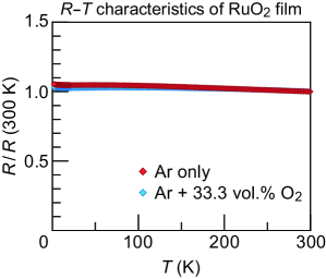
To check the effect of O2 gas introduction during sputtering on the RuO2 film, we also fabricated pristine (polycrystalline) RuO2 films under only Ar gas flow and also under a large amount of O2 gas flow (Ar + 33.3 vol.% O2, which is 5 times greater than that used for the RuO2AlOx deposition) and measured their – curves. Here, the RuO2 films were patterned into a Hall-bar shape having the length, width, and thickness of , , and , respectively, by sputtering RuO2 through a metal mask. Figure 6 shows the dependence of normalized by the value at 300 K for each RuO2 film. For both the films, the – curve shows almost the same characteristics; gradually increases with decreasing and the value at (the temperature of interest) deviates only 2% with each other. This result shows that the effect of oxygen on the RuO2 deposition does not play an essential role in the versus characteristics of RuO2.
APPENDIX B: COMPARISON OF CURVES BETWEEN RUO2ALOx FILMS ON SIO2/SI SUBSTRATES AND ON PT/YIG DEVICE
Figures 7(a) and 7(b) show the double logarithmic plot of (a) the resistivity and (b) its slope versus temperature for the RuO2AlOx films on thermally-oxidized Si substrates (filled circles) and on the Pt/YIG sample (red star marks) grown under the several d.c. sputtering power for the RuO2 target () and the fixed d.c. power for the Al target (). Although a small deviation of the and values is observed even under the same growth condition depending on the substrate layer (i.e., SiO2/Si or Pt/YIG), the overall dependent feature agrees well with each other. Note that the substrate-dependent difference in the and values does not have a significant impact on the observation of the cryogenic SPE, if the sensitivity is large enough for its detection.
References
- (1) H. Ohno, M. D. Stiles, and B. Dieny, Spintronics, Proc. IEEE 104, 1782 (2016).
- (2) A. V. Chumak, P. Kabos, M. Wu, C. Abert, C. Adelmann, A. O. Adeyeye, J. Åkerman, F. G. Aliev, A. Anane, A. Awad et al., Advances in magnetics roadmap on spin-wave computing, IEEE Trans. Magn. 58, 0800172 (2022).
- (3) H. Yang, S. O. Valenzuela, M. Chshiev, S. Couet, B. Dieny, B. Dlubak, A. Fert, K. Garello, M. Jamet, D.-E. Jeong, K. Lee, T. Lee, M.-B. Martin, G. S. Kar, P. Sénéor, H.-J. Shin, and S. Roche, Two-dimensional materials prospects for non-volatile spintronic memories, Nature 606, 663 (2022).
- (4) S. Maekawa, T. Kikkawa, H. Chudo, J. Ieda, and E. Saitoh, Spin and spin current–From fundamentals to recent progress, J. Appl. Phys. 133, 020902 (2023).
- (5) Y. Fan, P. Upadhyaya, X. Kou, M. Lang, S. Takei, Z. Wang, J. Tang, L. He, L.-T. Chang, M. Montazeri, G. Yu, W. Jiang, T. Nie, R. N. Schwartz, Y. Tserkovnyak, and K. L. Wang, Magnetization switching through giant spin-orbit torque in a magnetically doped topological insulator heterostructure, Nat. Mater. 13, 699 (2014).
- (6) J. Linder and J. W. A. Robinson, Superconducting spintronics, Nat. Phys. 11, 307 (2015).
- (7) M. Umeda, Y. Shiomi, T. Kikkawa, T. Niizeki, J. Lustikova, S. Takahashi, and E. Saitoh, Spin-current coherence peak in superconductor/magnet junctions, Appl. Phys. Lett. 112, 232601 (2018).
- (8) Y. Yao, Q. Song, Y. Takamura, J. P. Cascales, W. Yuan, Y. Ma, Y. Yun, X. C. Xie, J. S. Moodera, and W. Han, Probe of spin dynamics in superconducting NbN thin films via spin pumping, Phys. Rev. B 97, 224414 (2018).
- (9) Y. Shiomi, J. Lustikova, S. Watanabe, D. Hirobe, S. Takahashi, and E. Saitoh, Spin pumping from nuclear spin waves, Nat. Phys. 15, 22 (2019).
- (10) K.-R. Jeon, J.-C. Jeon, X. Zhou, A. Migliorini, J. Yoon, and S. S. P. Parkin, Giant Transition-State Quasiparticle Spin-Hall Effect in an Exchange-Spin-Split Superconductor Detected by Nonlocal Magnon Spin Transport, ACS Nano 14, 15874 (2020).
- (11) C. L. Tschirhart, E. Redekop, L. Li, T. Li, S. Jiang, T. Arp, O. Sheekey, T. Taniguchi, K. Watanabe, M. E. Huber, K. F. Mak, J. Shan, and A. F. Young, Intrinsic spin Hall torque in a moiré Chern magnet, Nat. Phys. 19, 807 (2023).
- (12) K. Uchida, H. Adachi, T. Kikkawa, A. Kirihara, M. Ishida, S. Yorozu, S. Maekawa, and E. Saitoh, Thermoelectric generation based on spin Seebeck effects, Proc. IEEE 104, 1946 (2016)., ibid. 104, 1499 (2016).
- (13) S. M. Rezende, Fundamentals of Magnonics (Springer Nature Switzerland AG, Switzerland, 2020).
- (14) T. Kikkawa and E. Saitoh, Spin Seebeck Effect: Sensitive Probe for Elementary Excitation, Spin Correlation, Transport, Magnetic Order, and Domains in Solids, Annu. Rev. Condens. Matter Phys. 14, 129 (2023).
- (15) T. Kikkawa, K. Shen, B. Flebus, R. A. Duine, K. Uchida, Z. Qiu, G. E. W. Bauer, and E. Saitoh, Magnon Polarons in the Spin Seebeck Effect, Phys. Rev. Lett. 117, 207203 (2016).
- (16) L. J. Cornelissen, K. Oyanagi, T. Kikkawa, Z. Qiu, T. Kuschel, G. E. W. Bauer, B. J. van Wees, and E. Saitoh, Nonlocal magnon-polaron transport in yttrium iron garnet, Phys. Rev. B 96, 104441 (2017).
- (17) K. Oyanagi, T. Kikkawa, and E. Saitoh, Magnetic field dependence of the nonlocal spin Seebeck effect in Pt/YIG/Pt systems at low temperatures, AIP Adv. 10, 015031 (2020).
- (18) J. Li, H. T. Simensen, D. Reitz, Q. Sun, W. Yuan, C. Li, Y. Tserkovnyak, A. Brataas, and J. Shi, Observation of Magnon Polarons in a Uniaxial Antiferromagnetic Insulator, Phys. Rev. Lett. 125, 217201 (2020).
- (19) T. Kikkawa, K. Oyanagi, T. Hioki, M. Ishida, Z. Qiu, R. Ramos, Y. Hashimoto, and E. Saitoh, Composition-tunable magnon-polaron anomalies in spin Seebeck effects in epitaxial films, Phys. Rev. Materials 6, 104402 (2022).
- (20) S. Geprägs, A. Kehlberger, F. D. Coletta, Z. Qiu, E.-J. Guo, T. Schulz, C. Mix, S. Meyer, A. Kamra, M. Althammer, H. Huebl, G. Jakob, Y. Ohnuma, H. Adachi, J. Barker, S. Maekawa, Gerrit E. W. Bauer, E. Saitoh, R. Gross, S. T. B. Goennenwein, and M. Kläui, Origin of the spin Seebeck effect in compensated ferrimagnets, Nat. Commun. 7, 10452 (2016).
- (21) W. Yuan, Q. Zhu, T. Su, Y. Yao, W. Xing, Y. Chen, Y. Ma, X. Lin, J. Shi, R. Shindou, X. C. Xie, and W. Han, Experimental signatures of spin superfluid ground state in canted antiferromagnet Cr2O3 via nonlocalspin transport, Sci. Adv. 4, eaat1098 (2018).
- (22) S. M. Wu, J. E. Pearson, and A. Bhattacharya, Paramagnetic Spin Seebeck Effect, Phys. Rev. Lett. 114, 186602 (2015).
- (23) K. Oyanagi, S. Takahashi, T. Kikkawa, and E. Saitoh, Mechanism of paramagnetic spin Seebeck effect, Phys. Rev. B 107, 014423 (2023).
- (24) D. Hirobe, M. Sato, T. Kawamata, Y. Shiomi, K. Uchida, R. Iguchi, Y. Koike, S. Maekawa, and E. Saitoh, One-dimensional spinon spin currents, Nat. Phys. 13, 30 (2017).
- (25) Y. Chen, M. Sato, Y. Tang, Y. Shiomi, K. Oyanagi, T. Masuda, Y. Nambu, M. Fujita, E. Saitoh, Triplon current generation in solids, Nat. Commun. 12, 5199 (2021).
- (26) W. Xing, R. Cai, K. Moriyama, K. Nara, Y. Yao, W. Qiao, K. Yoshimura, and W. Han, Spin Seebeck effect in quantum magnet Pb2V3O9, Appl. Phys. Lett. 120, 042402 (2022).
- (27) T. Kikkawa, D. Reitz, H. Ito, T. Makiuchi, T. Sugimoto, K. Tsunekawa, S. Daimon, K. Oyanagi, R. Ramos, S. Takahashi, Y. Shiomi, Y. Tserkovnyak, and E. Saitoh, Observation of nuclear-spin Seebeck effect, Nat. Commun. 12, 4356 (2021).
- (28) J. Flipse, F. K. Dejene, D. Wagenaar, G. E. W. Bauer, J. Ben Youssef, and B. J. van Wees, Observation of the Spin Peltier Effect for Magnetic Insulators, Phys. Rev. Lett. 113, 027601 (2014).
- (29) S. Daimon, R. Iguchi, T. Hioki, E. Saitoh, and K. Uchida, Thermal imaging of spin Peltier effect, Nat. Commun. 7, 13754 (2016).
- (30) S. Daimon, K. Uchida, R. Iguchi, T. Hioki, and E. Saitoh, Thermographic measurements of the spin Peltier effect in metal/yttrium-iron-garnet junction systems, Phys. Rev. B 96, 024424 (2017).
- (31) R. Itoh, R. Iguchi, S. Daimon, K. Oyanagi, K. Uchida, and E. Saitoh, Magnetic-field-induced decrease of the spin Peltier effect in Pt/Y3Fe5O12 system at room temperature, Phys. Rev. B 96, 184422 (2017).
- (32) A. Yagmur, R. Iguchi, S. Geprägs, A. Erb, S. Daimon, E. Saitoh, R. Gross, and K. Uchida, Lock-in thermography measurements of the spin Peltier effect in a compensated ferrimagnet and its comparison to the spin Seebeck effect, J. Phys. D: Appl. Phys. 51, 194002 (2018).
- (33) A. Sola, V. Basso, M. Kuepferling, C. Dubs, and M. Pasquale, Experimental proof of the reciprocal relation between spin Peltier and spin Seebeck effects in a bulk YIG/Pt bilayer, Sci. Rep. 9, 2047 (2019).
- (34) R. Yahiro, T. Kikkawa, R. Ramos, K. Oyanagi, T. Hioki, S. Daimon, and E. Saitoh, Magnon polarons in the spin Peltier effect, Phys. Rev. B 101, 024407 (2020).
- (35) T. Yamazaki, R. Iguchi, T. Ohkubo, H. Nagano, and K. Uchida, Transient response of the spin Peltier effect revealed by lock-in thermoreflectance measurements, Phys. Rev. B 101, 020415(R) (2020).
- (36) S. Daimon, K. Uchida, N. Ujiie, Y. Hattori, R. Tsuboi, and E. Saitoh, Thickness dependence of spin Peltier effect visualized by thermal imaging technique, Appl. Phys. Express 13, 103001 (2020).
- (37) K. Uchida, Transport phenomena in spin caloritronics, Proc. Jpn. Acad., Ser. B 97, 69 (2021).
- (38) K. Uchida and R. Iguchi, Spintronic Thermal Management, J. Phys. Soc. Japan 90, 122001 (2021).
- (39) A. Takahagi, R. Iguchi, H. Nagano, and K. Uchida, Highly sensitive lock-in thermoreflectance temperature measurement using thermochromic liquid crystal, Appl. Phys. Lett. 122, 172401 (2023).
- (40) Cernox Sensors Catalog, Cryogenic temperature sensor characteristics, Cernox vs. Rox Sensor Performance, in Temperature Sensor Information, Lake Shore https://www.lakeshore.com/resources/sensors
- (41) F. Pobell, Chapter 12: Low-Temperature Thermometry in Matter and Methods at Low Temperatures (Springer-Verlag Berlin Heidelberg, Heidelberg, 2007).
- (42) W. A. Bosch, F. Mathu, H. C. Meijer, and R. W. Willekers, Behaviour of thick film resistors (Philips type RC-01) as low temperature thermometers in magnetic fields up to 5 T, Cryogenics 26, 3 (1986).
- (43) Q. Li, C. H. Watson, R. G. Goodrich, D. G. Haase, and H. Lukefahr, Thick film chip resistors for use as low temperature thermometers, Cryogenics 26, 467 (1986).
- (44) I. Bat’ko, K. Flachbart, M. Somora, and D. Vanický, Design of RuO2-based thermometers for the millikelvin temperature range, Cryogenics 35, 105 (1995).
- (45) B. Neppert and P. Esquinazi, Temperature and magnetic field dependence of thick-film resistor thermometers (Dale type RC550), Cryogenics 36, 231 (1996).
- (46) M. Affronte, M. Campani, S. Piccinini, M. Tamborin, B. Morten, M. Prudenziati, and O. Laborde, Low Temperature Electronic Transport in RuO2-Based Cermet Resistors, J. Low Temp. Phys. 109, 461 (1997).
- (47) Y.-Y. Chen, Low-temperature Ru-Sapphire Film Thermometer and Its Application in Heat Capacity Measurements, AIP Conf. Proc. 684, 387 (2003).
- (48) Y. Y. Chen, P. C. Chen, C. B. Tsai, K. I. Suga, and K. Kindo, Low-Magnetoresistance RuO2Al2O3 Thin-Film Thermometer and its Application, Int. J. Thermophys. 30, 316 (2009).
- (49) J. Nelson and A. M. Goldman, Thin film cryogenic thermometers defined with optical lithography for thermomagnetic measurements on films, Rev. Sci. Instrum. 86, 053902 (2015).
- (50) S. Maniv and W. D. Westwood, Oxidation of an aluminum magnetron sputtering target in Ar/O2 mixtures, J. Appl. Phys. 51, 718 (1980).
- (51) E. Wallin and U. Helmersson, Hysteresis-free reactive high power impulse magnetron sputtering, Thin Solid Films 516, 6398 (2008).
- (52) Except for this procedure, we do not need to be extremely careful about the maintenance of the RuO2 and Al targets. As a side note, during the pre-sputtering process, RuO2 thin flakes that are easily peeled off may form on the shutter in the sputtering chamber, so we need to clean it regularly to prevent these flakes from falling on the RuO2 target.
- (53) M. Voigt and M. Sokolowski, Electrical properties of thin rf sputtered aluminum oxide films, Mater. Sci. Eng.: B 109, 99 (2004).
- (54) Since the SPE measurement in this study was intended to be performed at 2 K, the conditions for the thermometer fabrication were chosen to realize high sensitivity at 2 K. Our method can be extended to different temperatures by making thermometer films with high sensitivity at the targeted temperature range. However, as the temperature is lowered toward zero kelvin, the SPE-induced temperature difference is expected to decrease because the population of thermal magnons in YIG is suppressed.
- (55) A Hoffmann, Spin Hall Effects in Metals, IEEE Trans. Magn. 49, 5172 (2013).
- (56) J. Sinova, S. O. Valenzuela, J. Wunderlich, C. H. Back, and T. Jungwirth, Spin Hall effects, Rev. Mod. Phys. 87, 1213 (2015).
- (57) M. Schreier, G. E. W. Bauer, V. I. Vasyuchka, J. Flipse, K. Uchida, J. Lotze, V. Lauer, A. V. Chumak, A. A. Serga, S. Daimon, T. Kikkawa, E. Saitoh, B. J. van Wees, B. Hillebrands, R. Gross, and S. T. B. Goennenwein, Sign of inverse spin Hall voltages generated by ferromagnetic resonance and temperature gradients in yttrium iron garnet platinum bilayers, J. Phys. D: Appl. Phys. 48, 025001 (2015).
- (58) The Joule-heating-induced temperature increase under a typical value of 0.15 mA is less than 10 mK, which was confirmed by measuring the value of the RuO2AlOx film under the d.c. current of 0.15 mA applied to the Pt wire at and by comparing it with the – calibration curve shown in Fig. 4(d). The current value of 0.15 mA was adopted such that the sample’s temperature increase is less than 1% compared to the base temperature of 2 K and also that the SPE signal can be measured with a sufficient signal-to-noise ratio.
- (59) For the delay time of and the data acquisition time , the frequency of the applied square-wave current is estimated to be .
- (60) N. F. Mott, Conduction in non-crystalline materials III. Localized states in a pseudogap and near extremities of conduction and valence bands, Philos. Mag. 19, 835 (1969).
- (61) V. Ambegaokar, B. I. Halperin, and J. S. Langer, Hopping Conductivity in Disordered Systems, Phys. Rev. B 4, 2612 (1971).
- (62) R. Rosenbaum, Crossover from Mott to Efros-Shklovskii variable-range-hopping conductivity in films, Phys. Rev. B 44, 3599 (1991).
- (63) S. Lafuerza, J. García, G. Subías, J. Blasco, K. Conder, and E. Pomjakushina, Intrinsic electrical properties of LuFe2O4, Phys. Rev. B 88, 085130 (2013).
- (64) C. Lu, A. Quindeau, H. Deniz, D. Preziosi, D. Hesse, and M. Alexe, Crossover of conduction mechanism in Sr2IrO4 epitaxial thin films, Appl. Phys. Lett. 105, 082407 (2014).
- (65) X. Chen, B. Wang, Y. Chen, H. Wei, and B. Cao, Tuning JahnTeller distortion and electron localization of LaMnO3 epitaxial films via substrate temperature, J. Phys. D: Appl. Phys. 54, 235302 (2021).
- (66) Y. Li, M. You, X. Li, B. Yang, Z. Lin, and J. Liu, Tunable sensitivity of zirconium oxynitride thin-film temperature sensor modulated by film thickness, J. Mater. Sci.: Mater. Electron. 33, 20940 (2022).
- (67) C. T. Harris and T.-M. Lu, A PtNiGe resistance thermometer for cryogenic applications, Rev. Sci. Instrum. 92, 054904 (2021).
- (68) E. A. Scott, C. M. Smyth, M. K. Singh, T.-M. Lu, P. Sharma, D. Pete, J. Watt, and C. T. Harris, Optimization of gold germanium (Au0.17Ge0.83) thin films for high sensitivity resistance thermometry, J. Appl. Phys. 132, 065103 (2022).
- (69) S. S. Courts and P. R. Swinehart, Review of Cernox™(Zirconium Oxy-Nitride) Thin-Film Resistance Temperature Sensors, AIP Conf. Proc. 684, 393 (2003).
- (70) J. R. Clement and E. H. Quinnell, The Low Temperature Characteristics of Carbon-Composition Thermometers, Rev. Sci. Instrum. 23, 213 (1952).
- (71) W. N. Lawless, Thermometric Properties of Carbon-Impregnated Porous Glass at Low Temperatures, Rev. Sci. Instrum. 43, 1743 (1972).
- (72) A typical error at each field is evaluated to be for the data under , so the slight undulation behavior of above is attributed to the uncertainty of the measurement.
- (73) T. Kikkawa, M. Suzuki, J. Okabayashi, K. Uchida, D. Kikuchi, Z. Qiu, and E. Saitoh, Detection of induced paramagnetic moments in Pt on Y3Fe5O12 via x-ray magnetic circular dichroism, Phys. Rev. B 95, 214416 (2017).
- (74) K. Uchida, J. Ohe, T. Kikkawa, S. Daimon, D. Hou, Z. Qiu, and E. Saitoh, Intrinsic surface magnetic anisotropy in Y3Fe5O12 as the origin of low-magnetic-field behavior of the spin Seebeck effect, Phys. Rev. B 92, 014415 (2015).
- (75) T. Kikkawa, K. Uchida, S. Daimon, Z. Qiu, Y. Shiomi, and E. Saitoh, Critical suppression of spin Seebeck effect by magnetic fields, Phys. Rev. B 92, 064413 (2015).
- (76) H. Jin, S. R. Boona, Z. Yang, R. C. Myers, and J. P. Heremans, Effect of the magnon dispersion on the longitudinal spin Seebeck effect in yttrium iron garnets, Phys. Rev. B 92, 054436 (2015).
- (77) T. Kikkawa, K. Uchida, S. Daimon, and E. Saitoh, Complete Suppression of Longitudinal Spin Seebeck Effect by Frozen Magnetization Dynamics in Y3Fe5O12, J. Phys. Soc. Japan 85, 065003 (2016).
- (78) H. Adachi, K. Uchida, E. Saitoh, and S. Maekawa, Theory of the spin Seebeck effect, Rep. Prog. Phys. 76, 036501 (2013).
- (79) S. A. Bender and Y. Tserkovnyak, Interfacial spin and heat transfer between metals and magnetic insulators, Phys. Rev. B 96, 134412 (2015).
- (80) L. J. Cornelissen, K. J. H. Peters, G. E. W. Bauer, R. A. Duine, and B. J. van Wees, Magnon spin transport driven by the magnon chemical potential in a magnetic insulator, Phys. Rev. B 94, 014412 (2016).
- (81) Y. Ohnuma, M. Matsuo, and S. Maekawa, Theory of the spin Peltier effect, Phys. Rev. B 96, 134412 (2017).
- (82) K. Kanahashi, J. Pu, and T. Takenobu, 2D Materials for Large-Area Flexible Thermoelectric Devices, Adv. Energy Mater. 10, 1902842 (2020).
- (83) D. Li, Y. Gong, Y. Chen, J. Lin, Q. Khan, Y. Zhang, Y. Li, H. Zhang, and H. Xie, Recent Progress of Two-Dimensional Thermoelectric Materials, Nano-Micro Lett. 12, 36 (2020).
- (84) Q. H. Wang, A. Bedoya-Pinto, M. Blei, A. H. Dismukes, A. Hamo, S. Jenkins, M. Koperski, Y. Liu, Q.-C. Sun, E. J. Telford et al., The Magnetic Genome of Two-Dimensional van der Waals Materials, ACS Nano 16, 6960 (2022).