Cavity-coupled telecom atomic source in silicon
2Applied Physics Graduate Program, Smalley-Curl Institute, Rice University, Houston, TX 77005, USA
3Smalley-Curl Institute, Rice University, Houston, TX 77005, USA
)
Atomic defects in solid-state materials are promising candidates for quantum interconnect and networking applications. Recently, a series of atomic defects have been identified in the silicon platform, where scalable device integration can be enabled by mature silicon photonics and electronics technologies. In particular, T centers hold great promise due to their telecom band optical transitions and the doublet ground state electronic spin manifold with long coherence times. However, an open challenge for advancing the T center platform is to enhance its weak and slow zero phonon line emission. In this work, we demonstrate the cavity-enhanced fluorescence emission from a single T center. This is realized by integrating single T centers with a low-loss, small mode-volume silicon photonic crystal cavity, which results in an enhancement of the fluorescence decay rate by a factor of . Efficient photon extraction enables the system to achieve an average photon outcoupling rate of 73.3 kHz at the zero phonon line. The dynamics of the coupled system is well modeled by solving the Lindblad master equation. These results represent a significant step towards building efficient T center spin-photon interfaces for quantum information processing and networking applications.
Optically interfaced atomic defects in solid-state materials are promising candidates for a variety of quantum technologies [1]. In particular, nitrogen and silicon vacancy centers in diamond have been used to demonstrate milestone results for fiber-based quantum networks, including spin-photon entanglement [2], deterministic entanglement generation between remote spins [3], quantum state teleportation [4], and memory-enhanced communication [5]. However, these defects have optical transitions at the visible or near-infrared spectral range resulting in large fiber transmission loss, requiring nonlinear frequency conversion [6] to extend the network range. Significant progress has been made towards utilizing atomic defects with telecom optical transitions, leading to the discovery of single vanadium ions in silicon carbide [7] and single erbium ions in yttrium orthosilicate [8], as well as recent demonstration of indistinguishable telecom photon generation from single erbium ions [9].
Early exploration into scalable fabrication of atomic defects with photonic structures relies on heterogeneous material integration and typically involves pick-and-place type of fabrication procedures [10, 8, 11]. On the other hand, silicon-on-insulator (SOI) is a mature and scalable platform to enable large-scale monolithic photonic and electronic device integration. Telecom-interfaced solid-state spins in silicon can thus benefit from the technological advantages of the SOI platform, and be utilized for realizing large-scale spin-based integrated quantum photonic chips [12]. Moreover, silicon can be isotopically enriched to create a “semiconductor vacuum” [13] for lowering the magnetic noise generated from the 29Si nuclear spin bath.
Beyond efforts towards optical addressing of erbium ions in silicon [14, 15, 16], multiple novel atomic defect centers in silicon, including , , , and centers [17, 18, 19, 20, 21, 22, 23, 24, 25, 26], have been experimentally identified recently towards quantum information applications. Among them, T centers are particularly promising due to their telecom O-band optical transitions, doublet ground state spin manifold, and long spin coherence times in an enriched 28Si sample [22]. Single T centers have been isolated in micropuck [23] and waveguide [27] structures. To further advance the single T center platform for quantum networking applications, challenges remain to enhance its weak and slow coherent emission at the zero phonon line (ZPL). The cavity-induced Purcell effect [28] has been widely used for enhancing the fluorescence emission of various atomic defects in solids, including centers [29, 30, 31].
In this work, we demonstrate Purcell enhancement of a single T center in a low-loss, small mode-volume silicon photonic crystal (PC) cavity. When the cavity is tuned into resonance with the single T center we observe an enhancement of its fluorescence decay rate by a factor of , shortening the single T center’s lifetime to 136.4 0.6 ns. Leveraging the nanophotonic circuit and an angle-polished fiber for light coupling [32], the system detection efficiency reaches = 9.1%, representing the probability of a single photon emitted into the cavity being registered by the detector. This efficiency is 20-fold larger than that achieved in a typical confocal-type measurement system for T centers. We probe single T centers in the device using time-resolved photoluminescence excitation (PLE) spectroscopy. Under the pulsed excitation, the system can detect 0.01 ZPL photon per excitation, reaching an average photon count rate of 73.3 kHz, which is about two orders of magnitude improvement from previously reported emission rate for single T centers in the waveguide [27]. By solving the Lindblad master equation, we develop a numerical model to describe the coupling dynamics between the single T center and the cavity, and extract cavity-QED parameters as well as T center pure dephasing rate () and spectral diffusion (). This work represents a key step towards utilizing single T centers in silicon for quantum information applications.
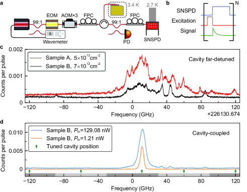
Our experimental configuration is outlined in Fig. 1a. The nanophotonic devices are fabricated on a SOI sample which is situated on the cold finger of a closed-cycle cryostat ( K). Each device consists of a subwavelength grating coupler (GC) [33] and a one-dimensional PC cavity, which are connected by a linearly tapered waveguide (Fig. 1b). Optical coupling to the PC cavities is accomplished by using an angle-polished fiber via the GC with an one-way coupling efficiency of % at 1326 nm (Fig. 1c). The fiber is mounted on a three-axis translation stage for optimizing the coupling. The PC cavity used in this work (Fig. 1d) has a quality factor . Fluorescence from the T center is detected by a fiber-coupled superconducting nanowire single photon detector (SNSPD) located in a separate cryostat (Fig. 2a). To match the atomic transition, we coarsely red-tune the cavity resonance by condensing nitrogen gas onto the surface of the device; we fine blue-tune the cavity resonance by sending laser pulses with a high optical power into the cavity [34].
T centers are generated in the middle of the device layer (220 nm in thickness) of the SOI samples using the ion implantation method [35]. Each SOI sample is implanted sequentially with 1:1 ratio of 35 keV 12C and 8 keV 1H ions, with rapid thermal annealing performed in-between and after the implantation steps [34]. The two samples shown in this work have an implantation fluence of cm-2 (sample A) and cm-2 (sample B), respectively. To search for T centers, we perform time-resolved PLE spectroscopy by scanning the wavemeter-stabilized laser around the reported inhomogeneous center of T centers in silicon [22, 35, 23], with the pulse sequence shown in Fig. 2b.
First, we measure the spectrum with the cavity far-detuned from the scan range (Fig. 2c). The inhomogeneous distribution linewidth is about GHz. Isolated peaks can be observed away from the inhomogeneous center, which we interpret as the optical transitions of T centers that are likely located inside the taper waveguide. These peaks have an average full width half maximum (FWHM) linewidth of GHz, and a fluorescence lifetime of ns [34], which is slightly shorter than the bulk T centers’ lifetime of 940 ns [22]. The estimated T center densities are cm-3 and cm-3 for sample A and B, respectively [34]. For a specific waveguide-coupled T center (at 46 GHz) in sample B, we use the bounded T center quantum efficiency (discussed below) to estimate its emission efficiency to the waveguide mode as % [34].
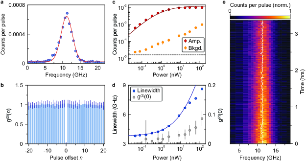
Next, we scan the laser frequency with the cavity tuned in-range to obtain the cavity-coupled PLE spectrum (Fig. 2d). In sample B, a new T center peak at the inhomogeneous center emerges with its fluorescence significantly surpassing all other peaks. This cavity-coupled T center has a FWHM linewidth of GHz under a low excitation power (Fig. 3a). To verify the peak originates from a single T center, we measure the second-order autocorrelation function using all the detected fluorescence photons after each excitation pulse (Fig. 3b). Photon antibunching is observed with the value , which confirms the majority of the detected photons come from a single emitter. Autocorrelation measurements for the single T center can show bunching (, when ) under certain excitation conditions, which we speculate to be caused by the spectral diffusion [34].
The emission amplitude of the cavity-coupled single T center saturates at 0.01 photons per excitation pulse (Fig. 3c). Both the saturation and power dependent linewidth (Fig. 3d) are well described by the numerical modeling (discussed below). The measured at higher powers (Fig. 3d) is limited by the accidental coincidences from background T centers’ emission [34]. To characterize the spectral diffusion, we monitor the spectrum of the cavity-coupled single T center over a few hours time span by taking repetitive PLE scans (Fig. 3e), which reveals a spectrum-center distribution of GHz. A similar level of spectral diffusion is observed for waveguide-coupled T centers [34]. We note that this method only provides a lower bound of the due to the limited experiment repetition rate. We later turn to the numerical modeling to extract .
We apply a magnetic field () up to 300 mT along silicon direction aiming to split the single T center line. We note that we have not been able to observe unambiguous Zeeman splitting using simultaneous two-tone laser sideband excitation [34], which is likely due to the limited splitting compared with the broad single T center linewidth. When using the single-tone laser excitation, the PLE amplitude decreases at increasing field due to spin polarization [35]. We model this behavior [34] to extract the difference of the excited- and ground-state -factors , which matches with one of the two predicted values for T centers under a field along the silicon direction [35].
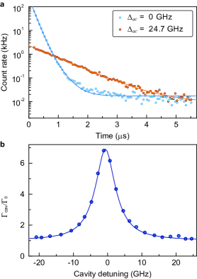
Lastly, we study the cavity-QED of the coupled system. When the cavity is tuned into resonance, the single T center’s fluorescence lifetime is shortened to ns (Fig. 4a), which is times faster than the bulk lifetime of ns [22]. Leveraging this enhanced decay, we extract an average ZPL photon outcoupling rate of 73.3 kHz at saturation for the cavity-coupled single T center. To confirm the enhancement originates from the cavity coupling, we measure the fluorescence decay rate at different cavity detunings () (Fig. 4b), which can be described as , where is the Purcell factor describing the fluorescence decay enhancement due to the cavity, is the asymptotic decay rate at large detunings, and GHz is the characteristic linewidth. To explain the deviation of from the cavity linewidth GHz, we turn to numerical calculations by solving the Lindblad master equation. Beyond the cavity and atomic loss channels, we also incorporate the pure dephasing and spectral diffusion processes [34]. The dynamics of the coupled system can be described by the Jaynes-Cummings Hamiltonian of the form,
| (1) |
which assumes rotating wave approximation in the rotating frame of the laser field (). Here and are, respectively, the detunings of the laser from the T center transition and the cavity resonance ; is the coupling rate between the single T center and the cavity mode, and is the optical Rabi frequency. The global fitting of the experimental data based on the numerical calculations [34] reveals the cavity-QED parameters (42.4 MHz, 5.22 GHz, 169.3 kHz), an excited-state dephasing rate GHz and a spectral diffusion GHz. The characteristic linewidth has contributions from the cavity linewidth as well as and . The model can simultaneously capture the saturation (Fig. 3c), power-dependent linewidth (Fig. 3d), and detuning-dependent fluorescence decay (Fig. 4b) results. Beyond the dephasing and the spectral diffusion, the single T center linewidth also has a minor contribution from the thermal broadening, which we estimate as GHz from the temperature-dependent linewidth measurements [34].
To find out the Purcell enhancement of the single T center’s ZPL () and its quantum efficiency (), we express the total emission rate of a single T center in absence of a cavity as the summation of the emission rates into the ZPL and the phonon sideband (PSB), as well as nonradiative relaxation [36], . The Debye-Waller (DW) factor and the quantum efficiency can then be defined as DW = and , respectively. When the cavity is tuned into resonance with the T center ZPL, the cavity enhanced decay rate is , where is the Purcell factor describing the enhancement of the ZPL. We can thus put a lower bound on the , using the reported DW of 23% [22]. For simplicity, we neglect the potential suppression of the due to the cavity [36]. The ratio of the single T center ZPL emission coupled to the resonant cavity mode can be estimated as %. Due to sub-optimal positioning of the single T center inside the cavity and imperfect dipole alignment with the local cavity electrical field polarization, the extracted from measurements should be smaller than the simulated Purcell (). This enables us to put a lower bound on the quantum efficiency % for the single T center [34].
We now discuss pathways to improve the performance of the cavity-coupled single T center system. Due to technical difficulties, the first 170 ns of the fluorescence signal cannot be collected. The fluorescence count level can be improved by a factor of 2.5 by using AOMs with a faster switching speed. We note that the linewidth of the observed single T center is significantly larger than the Purcell enhanced lifetime-limited linewidth (2 MHz). One culprit is the fast dephasing process, which necessitates further investigation to reveal its origin. Significant reduction of down to 33 MHz has been demonstrated for ensemble T centers in enriched 28Si [22]. In future work, SOI samples with an enriched silicon device layer can be prepared via molecular beam epitaxy [37] to minimize the dephasing. Furthermore, local electrodes can be fabricated on the SOI device layer for implementing electrical field control to minimize the spectral diffusion via in situ tuning [38] or depletion of the charge noises [39]. Lastly, focused-ion-beam-based [40] and masked [41] ion implantation can be leveraged to increase the yield of T center generation at the cavity center.
In summary, we have demonstrated enhanced light-matter interaction for a single T center by integrating it with a silicon nanophotonic cavity. This work opens the door to utilize single T centers in silicon for quantum information processing and networking applications. With realistic improvements in the quality factor of the optical cavity () and narrower linewidth in an enriched sample ( 10 MHz), a large atom-cavity cooperativity can be expected, which can lead to applications for high-fidelity dispersive spin readout [42] and cavity-mediated spin-spin interactions [43]. Moreover, the current approach can enable parallel control and readout of multiple T centers in the cavity via the frequency domain addressing technique [44]. Finally, leveraging the mature silicon photonics technology, small-footprint and scalable T-center-spin-based silicon quantum photonic chips [12] may be envisioned.
Note: While finalizing this manuscript, we became aware of a related publication on detection of a single T center coupled to a cavity using above-band excitation [45].
Acknowledgements
We gratefully acknowledge Han Pu, Alexey Belyanin, and Tanguy Terlier for helpful discussions, and John Bartholomew for feedback on a manuscript draft. Support for this research was provided by the National Science Foundation (NSF, CAREER Award No. 2238298), the Robert A. Welch Foundation (Grant No. C-2134) and the Rice Faculty Initiative Fund. We acknowledge the use of cleanroom facilities supported by the Shared Equipment Authority at Rice University.
Data Availability
The datasets generated and/or analyzed during the current study are available from the corresponding author on reasonable request.
Competing interests
The authors declare no competing interests.

References
- [1] Awschalom, D. D., Hanson, R., Wrachtrup, J. & Zhou, B. B. Quantum technologies with optically interfaced solid-state spins. Nat. Photon. 12, 516–527 (2018).
- [2] Togan, E. et al. Quantum entanglement between an optical photon and a solid-state spin qubit. Nature 466, 730–734 (2010).
- [3] Bernien, H. et al. Heralded entanglement between solid-state qubits separated by three metres. Nature 497, 86–90 (2013).
- [4] Pfaff, W. et al. Unconditional quantum teleportation between distant solid-state quantum bits. Science 345, 532–535 (2014).
- [5] Bhaskar, M. K. et al. Experimental demonstration of memory-enhanced quantum communication. Nature 580, 60–64 (2020).
- [6] Li, Q., Davanço, M. & Srinivasan, K. Efficient and low-noise single-photon-level frequency conversion interfaces using silicon nanophotonics. Nat. Photon. 10, 406–414 (2016).
- [7] Wolfowicz, G. et al. Vanadium spin qubits as telecom quantum emitters in silicon carbide. Sci. Adv. 6, eaaz1192 (2020).
- [8] Dibos, A., Raha, M., Phenicie, C. & Thompson, J. D. Atomic source of single photons in the telecom band. Phys. Rev. Lett. 120, 243601 (2018).
- [9] Ourari, S. et al. Indistinguishable telecom band photons from a single Er ion in the solid state. Nature 620, 977–981 (2023).
- [10] Kim, J.-H. et al. Hybrid integration of solid-state quantum emitters on a silicon photonic chip. Nano Lett. 17, 7394–7400 (2017).
- [11] Wan, N. H. et al. Large-scale integration of artificial atoms in hybrid photonic circuits. Nature 583, 226–231 (2020).
- [12] Pelucchi, E. et al. The potential and global outlook of integrated photonics for quantum technologies. Nat. Rev. Phys. 4, 194–208 (2022).
- [13] Steger, M. et al. Quantum information storage for over 180 s using donor spins in a 28Si “semiconductor vacuum”. Science 336, 1280–1283 (2012).
- [14] Yin, C. et al. Optical addressing of an individual erbium ion in silicon. Nature 497, 91–94 (2013).
- [15] Gritsch, A., Weiss, L., Früh, J., Rinner, S. & Reiserer, A. Narrow optical transitions in erbium-implanted silicon waveguides. Phys. Rev. X 12, 041009 (2022).
- [16] Berkman, I. R. et al. Millisecond electron spin coherence time for erbium ions in silicon. arXiv preprint arXiv:2307.10021 (2023).
- [17] Chartrand, C. et al. Highly enriched 28Si reveals remarkable optical linewidths and fine structure for well-known damage centers. Phys. Rev. B 98, 195201 (2018).
- [18] Beaufils, C. et al. Optical properties of an ensemble of G-centers in silicon. Phys. Rev. B 97, 035303 (2018).
- [19] Redjem, W. et al. Single artificial atoms in silicon emitting at telecom wavelengths. Nat. Electron. 3, 738–743 (2020).
- [20] Komza, L. et al. Indistinguishable photons from an artificial atom in silicon photonics. arXiv preprint arXiv:2211.09305 (2022).
- [21] Prabhu, M. et al. Individually addressable and spectrally programmable artificial atoms in silicon photonics. Nat. Commun. 14, 2380 (2023).
- [22] Bergeron, L. et al. Silicon-integrated telecommunications photon-spin interface. PRX Quantum 1, 020301 (2020).
- [23] Higginbottom, D. B. et al. Optical observation of single spins in silicon. Nature 607, 266–270 (2022).
- [24] DeAbreu, A. et al. Waveguide-integrated silicon T centres. Opt. Express 31, 15045–15057 (2023).
- [25] Tait, A. N. et al. Microring resonator-coupled photoluminescence from silicon W centers. J. Phys. Photonics 2, 045001 (2020).
- [26] Baron, Y. et al. Detection of single W-centers in silicon. ACS Photon. 9, 2337–2345 (2022).
- [27] Lee, C.-M. et al. High-efficiency single photon emission from a silicon T-center in a nanobeam. arXiv preprint arXiv:2308.04541 (2023).
- [28] Purcell, E. M. Spontaneous emission probabilities at radio frequencies. In Confined Electrons and Photons: New Physics and Applications, 839–839 (Springer, 1995).
- [29] Lefaucher, B. et al. Cavity-enhanced zero-phonon emission from an ensemble of G centers in a silicon-on-insulator microring. Appl. Phys. Lett. 122 (2023).
- [30] Redjem, W. et al. All-silicon quantum light source by embedding an atomic emissive center in a nanophotonic cavity. Nat. Commun. 14, 3321 (2023).
- [31] Saggio, V. et al. Cavity-enhanced single artificial atoms in silicon. arXiv preprint arXiv:2302.10230 (2023).
- [32] Chen, S. et al. Hybrid microwave-optical scanning probe for addressing solid-state spins in nanophotonic cavities. Opt. Express 29, 4902–4911 (2021).
- [33] Liu, L., Pu, M., Yvind, K. & Hvam, J. M. High-efficiency, large-bandwidth silicon-on-insulator grating coupler based on a fully-etched photonic crystal structure. Appl. Phys. Lett. 96 (2010).
- [34] See the supplementary materials .
- [35] MacQuarrie, E. et al. Generating T centres in photonic silicon-on-insulator material by ion implantation. N. J. of Phys. 23, 103008 (2021).
- [36] Johnson, S. et al. Tunable cavity coupling of the zero phonon line of a nitrogen-vacancy defect in diamond. N. J. Phys. 17, 122003 (2015).
- [37] Liu, Y. et al. 28Silicon-on-insulator for optically interfaced quantum emitters. J. Cryst. Growth 593, 126733 (2022).
- [38] Acosta, V. et al. Dynamic stabilization of the optical resonances of single nitrogen-vacancy centers in diamond. Phys. Rev. Lett. 108, 206401 (2012).
- [39] Anderson, C. P. et al. Electrical and optical control of single spins integrated in scalable semiconductor devices. Science 366, 1225–1230 (2019).
- [40] Schröder, T. et al. Scalable focused ion beam creation of nearly lifetime-limited single quantum emitters in diamond nanostructures. Nat. Commun. 8, 15376 (2017).
- [41] Toyli, D. M., Weis, C. D., Fuchs, G. D., Schenkel, T. & Awschalom, D. D. Chip-scale nanofabrication of single spins and spin arrays in diamond. Nano Lett. 10, 3168–3172 (2010).
- [42] Nguyen, C. et al. An integrated nanophotonic quantum register based on silicon-vacancy spins in diamond. Phys. Rev. B 100, 165428 (2019).
- [43] Evans, R. E. et al. Photon-mediated interactions between quantum emitters in a diamond nanocavity. Science 362, 662–665 (2018).
- [44] Chen, S., Raha, M., Phenicie, C. M., Ourari, S. & Thompson, J. D. Parallel single-shot measurement and coherent control of solid-state spins below the diffraction limit. Science 370, 592–595 (2020).
- [45] Islam, F. et al. Cavity enhanced emission from a silicon T center. arXiv preprint arXiv:2310.13808 (2023).