Strain Engineering for Transition Metal Defects in SiC
Abstract
Transition metal (TM) defects in silicon carbide (SiC) are a promising platform for applications in quantum technology as some of these defects, e.g. vanadium (V), allow for optical emission in one of the telecom bands. For other defects it was shown that straining the crystal can lead to beneficial effects regarding the emission properties. Motivated by this, we theoretically study the main effects of strain on the electronic level structure and optical electric-dipole transitions of the V defect in SiC. In particular we show how strain can be used to engineer the -tensor, electronic selection rules, and the hyperfine interaction. Based on these insights we discuss optical Lambda systems and a path forward to initializing the quantum state of strained TM defects in SiC.
I Introduction
A fundamental ingredient for many quantum technologies and experiments is a coherent interface between flying qubits and stationary quantum memories [1, 2, 3]. An established set of physical systems with great potential in this domain are so called color centers which are defects in solids with optical transitions. Color centers can often additionally be coupled to nearby nuclear spins that lend themselves to quantum memories or long-lived quantum registers.
The most studied color center is the negatively charged nitrogen-vacancy (NV) defect in diamond [4, 5, 6, 7, 8, 9, 10, 11, 12, 13, 14, 15, 16] ([17, 18, 19] for reviews). Optical initialization and readout of its electron spin state is made feasible by the spin-photon interface via its excited state [20]. Together with a coherent microwave manipulation, optically detected magnetic resonance (ODMR) is feasible in this defect [21]. Efficient coupling to nearby nuclear spins was demonstrated and utilized in long living quantum memory applications [11, 15, 16]. Despite its favorable spin and optical properties, contenders for host materials other than diamond are emerging. The most notable is silicon carbide (SiC) with advanced crystal growth [22], defect creation [23, 24], and micro-fabrication techniques readily available [25, 26, 27]. These technological advancements improve the scalability [28, 29] and magneto-optical properties of several hosted quantum defects, e.g. the negatively charged silicon vacancy [30, 31, 32] and the neutral divacancy [33, 34].
In this article, we focus on the transition metal (TM) defects in silicon-carbide (SiC), particularly on vanadium (V) defects. In contrast to the defects discussed in the previous paragraph, V defects in SiC feature a zero-phonon line (ZPL) within the telecom bands, favorable for minimal loss transmission using optical fibers. The focus of previous experiments [35, 36, 37, 38, 39, 40] and theory [41, 42, 43, 44, 45] for TM defects in SiC was on unstrained defects, however, the knowledge on the external perturbations effecting the magneto-optical properties of the quantum defects is a key ingredient in their applications [46, 47, 48, 49]. Strain can be used passively, e.g. to reduce the dispersive readout time in silicon vacancy centers in diamond [50] and to engineer the electronic structure [51] and -tensor [52], or actively to drive spin transitions in NV centers [46] as well as to create a hybrid quantum systems by coupling a mechanical oscillator to defects [53, 54].
Motivated by these prospects, in this work we aim to generalize the effective Hamiltonian to describe transition metal defects in silicon carbide under strain. To this end, we build on top of previous group-theory based results [42, 43] which were in good agreement with previous ab-initio calculations [41] and experimental findings [38, 37, 39, 40]. Additionally, we use density functional theory (DFT) calculations to estimate the strain coupling strength for the commonly used vanadium defect in the site of 4H-SiC 111 According to previous DFT results the site corresponds to the configuration of vanadium in 4H-SiC [41]. . We show how strain in these samples can be used to engineer the optical transition frequency, the -tensor, transition rules as well as the form of the hyperfine interaction. Based on this, we discuss state preparation and readout as well as microwave control in strained samples.
This paper is organized as follows. We begin by introducing the physical model for the V defect in SiC in Sec. II, including its effective Hamiltonian. Using this model, we combine and compare the effective Hamiltonian and ab initio calculations in Sec. III.1. Based on these results, we then show the possibility to engineer the -tensor (Sec. III.2), selection rules (Sec. III.3), and how these can be combined to create a Lambda system for pseudo-spin state preparation (Sec. III.4). In Sec. III.5, we discuss the influence of strain on the hyperfine interaction and how this influences the possibility to initialize the nuclear spin. We summarize our findings and present our conclusions in Sec. IV.
II Model
II.1 Defect structure
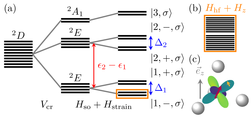
The defect energy levels, sketched in Fig. 1, can be described by a single electron in an orbital resembling the original atomic orbital. The levels are split by the crystal potential into two orbital doublets and one orbital singlet . Due to the spin-orbit interaction and the interaction with an external strain field, the orbital doublets are further split. This results in a level structure made up by five Kramers doublets (KDs) which are pairs of states related to each other by time inversion. We use a group theoretic model in the following to describe the above interactions within an effective Hamiltonian where we additionally calculate selection rules between the KDs, the hyperfine structure of the KDs, and the Zeeman term within each KD. Therein, we calculate the orbital-strain interaction parameters not yet reported in the literature using ab initio calculations and also use these to confirm predictions made by the effective Hamiltonian.
II.2 Effective Hamiltonian
We generalize the effective Hamiltonian from [42, 43, 45] to additionally include the strain such that the full Hamiltonian is of the form
| (1) |
where the form of the atomic Hamiltonian (), crystal potential , spin-orbit interaction , and coupling to magnetic and electric fields are discussed in [42]. The interaction with the central nuclear spin (of the TM) was derived and analyzed in [43]. We summarize the form of these terms below and additionally discuss the influence of strain within this symmetry-based framework. We note that this approach can only work in the domain where the strain can be viewed as a small perturbation compared to . As we show in the following, this restriction does not affect our conclusions, since significant strain effects are demonstrated within this domain.
In the basis of (orbital) eigenstates with of (introduced in [42]) and using the corresponding projections of degenerate subspaces and , we can write the combined atomic and crystal Hamiltonian as
| (2) |
where are the crystal energies. Here, labels the three orbital multiplets shown in Fig. 1(a). In the following, we describe each part of the Hamiltonian by its contribution to each of the nine blocks defined by the three orbital sectors ().
Using the projection operators, we can formulate the different blocks of the spin-orbit interaction as
| (3) | ||||
| (4) |
where , denote the Pauli matrices (here acting between the orbital states states ), and () the spin-1/2 operators of the electron in units of . The spin-orbit coupling constants are in units of energy with this convention.
Another relevant term is the electronic Zeeman interaction due to the spin and angular momentum coupling to an external magnetic field. In the relevant subspaces, it is given by
| (5) | ||||
| (6) |
where we use the electron gyromagnetic ratio , the Bohr magneton , and the coupling constants of the orbital Zeeman term .
The nuclear Hamiltonian (for transition metal defects with non-zero nuclear spin) is made up by the hyperfine interaction and the nuclear Zeeman interaction with the nuclear spin operator in units of , the nuclear magneton , and nuclear -factor . As the nuclear Zeeman term is proportional to the identity operator in the electronic subspace, it can be straightforwardly incorporated. Following [43] and accommodating to the notation employed in this article, the hyperfine interaction projected onto the relevant subspaces is
| (7) | ||||
| (8) |
where we use the ladder operators with as well as the set of hyperfine coupling parameters , , and .
The effect of an applied electric field can be described by
| (9) | ||||
| (10) |
with the coupling strengths .
Lastly, we turn to the strain Hamiltonian. In our model, we start with a product space of orbital and spin components, such that we can incorporate the strain interaction within the orbital subspace. Its competition with the spin-orbit interaction gives rise to a complex interplay within the KDs. To describe it, we use the assignment of the different strain elements to irreducible representations of [46] which then couple to the corresponding orbital operator, the strain components transforming like the basis of the irreducible representation couple to operators of the form of and , while the strain components transforming like the basis of couple to operators of the form of . With these considerations, the strain Hamiltonian
| (11) | ||||
| (12) |
has a similar structure as the coupling to electric fields but potentially leads to a much larger contribution. Here, we use the reduced components of the strain tensor, organized by symmetry, , , and . In contrast to the coupling to electric (and magnetic) fields, the tensorial form of the strain manifests itself in the presence of multiple strain elements pertaining to the same irreducible representation. These elements can also have different coupling constants and leading to more degrees of freedom than a coupling to vectors.
For concreteness, we focus on the vanadium defect in the site of 4H-SiC in the following. We use the already known combinations of parameters and we additionally estimate the magnitude of the strain coupling constants using DFT calculations. Many relevant parameters without strain can be found in our previous works [42, 43, 45], including their values for other defects.
III Results
In a first step, we investigate the electronic structure following from an externally applied, uniaxial, and static strain. The remaining terms in the Hamiltonian will be discussed afterwards, omitting the discussion of static electric fields as they couple weakly to the defect compared to strain and magnetic fields and the symmetry-based electric-field coupling Hamiltonian [Eqs. (9) and (10)] is similar to the strain Hamiltonian [Eqs. (11) and (12)].
Referring to the absence of an external electromagnetic field as “zero field”, we define the electronic zero-field Hamiltonian as . Projected onto one of the doublets, the electronic zero-field Hamiltonian is
| (13) |
where we take the crystal field splitting to be the dominant contribution, i.e. with , , and . Furthermore, we investigate the domain where the magnetic field is weak compared to the spin-orbit coupling, as is relevant for most experimental and technological applications. Therefore, we begin by diagonalizing the Hamiltonian (13), leading to the eigenvalues
| (14) |
with the combined spin-orbit and strain splitting . As it splits the orbital doublet into two Kramers doublets (made up by two pseudo spins) we refer to as the orbital splitting. These energies are doubly degenerate in agreement with Kramers’ theorem, as time-reversal symmetry is still preserved for this static Hamiltonian, despite the (potential) spatial symmetry breaking due to strain. The corresponding eigenstates are
| (15) |
where denotes the spin and is also used as to achieve a concise notation. The - and -like components of the strain coupling compete with each other and with the spin-orbit coupling, leading to the mixing angles and . Without strain, the symmetry of the defect is intact, yielding the KDs and for the and KDs, respectively.
III.1 Ab initio calculations
The defect structure shows point symmetry owing to the axial crystal field of the 4H polytype. It introduces a double-degenerate orbital inside the band gap, occupied by a single electron and two empty orbital levels ( and ) which are localized inside the conduction band in the ground state electronic configuration. The lowest energy excitation promotes the electron between the different levels, sinking the orbital inside the band gap. The calculated ZPL energy of 0.91 eV is in reasonable agreement with experiments [38]. We note that Jahn-Teller instabilities are suppressed in the calculations by a smeared occupation in the orbital subspace, describing a dynamically averaged system in the unperturbed solution and strain perturbation is applied to this high-symmetry system.
First, we determine the orbital-strain coupling constants, without spin-orbit coupling taken into account, in both the ground and first excited state of the defect. To this end, we apply strain with a magnitude of up to 0.02 and fit a linear response for the orbital level splitting energy and the ZPL energy in the case of and strain components, respectively. The coupling coefficients are extracted as the fitted slope. Within the margin of error (see App. A) the slope for strains transforming together agree and are predicted to have the same by the effective Hamiltonian, such that we will use their average in the following. The calculated values are collected in Table 1 where we additionally assigned the signs based on the discussion in App. B.
| () | () | ||
|---|---|---|---|
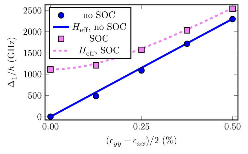
To confirm the agreement between the effective Hamiltonian and the ab initio calculations as well as the extrapolation of using the purely orbital calculations to extract the strain coupling constants we use these combined with the spin-orbit splitting in the absence of strain predicted by the ab initio calculation given by about GHz to calculate the ground state energy splitting and compare them to simulations combining strain and the spin-orbit interaction, see Fig. 2. The spin-orbit splitting calculated using DFT turns out to be about twice the experimentally measured value of GHz [38] in agreement with a Ham reduction factor of about [41].
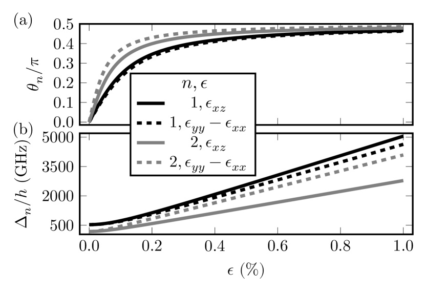
For this reason, we will use the numerically determined strain coupling constants but use experimentally determined parameters from the literature where available. In particular, we compare the mixing angle as well as the combined spin-orbit and strain splitting as functions of strain components transforming according to of the GS and ES doublets in Fig. 3 using the experimentally determined spin-orbit splittings GHz and GHz [38], where we assigned the signs based on the level ordering [43]. Fig. 3 shows that the splittings of the ES and GS diverge more for strain than for . The mixing angle between the strain types is also different where it increases faster for strain and in all cases approach the asymptotic value of which corresponds to maximal mixing of the unstrained KDs, see Eq. (15).
The linear dependence of Eq. (14) on -type strain, i.e. and , combined with the non-zero difference of the coupling constants between the GS and ES from the ab initio calculation (see Tab. 1) implies that -type strain can be used to tune the optical transition frequency, i.e. the crystal field splitting. This is possible while keeping the selection rules intact as -type strain conserves the defect’s symmetry. Within the effective Hamiltonian we choose to use because the overall energy shift can be set arbitrarily and only the energy differences contained in the effective Hamiltonian carry physical meaning. We assign the full difference of the coupling of the ES and GS orbital doublets extracted from the ab initio calculation to the parameters and .
III.2 Engineering the -tensor
Projecting onto the KD (spanned by the states with ) we calculate the leading-order Zeeman term
| (16) | ||||
with the effective -factors and , where is the pseudo-spin () operator for the KD. From this expression, it is evident that using strain enables coupling to perpendicular magnetic fields such that quantum gates relying on operators become possible using microwave drives. Furthermore, -type strain leads to an effective rotation of the spin in the plane regarding an external magnetic field.
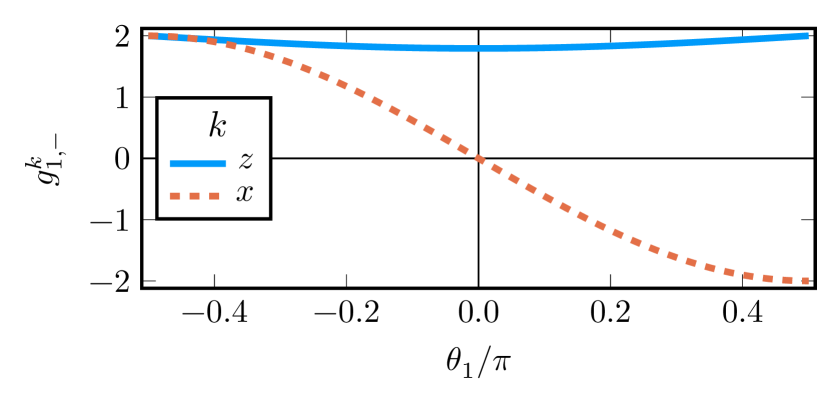
As we previously showed in the absence of strain [42], in the presence of strain the -factors are also influenced by (combined) higher orders of the strain and spin-orbit interactions between different orbital subspaces. We calculate the (second-order) correction using a Schrieffer-Wolf transformation treating as the perturbation. In App. C, we show how to derive the correction for for purely -type strain. These are in agreement with previous unstrained results. Using the insights of the higher order, we can calculate as the mean deviation from of the experimentally determined of the same doublet and attribute the remaining deviation to a common deviation from due to the second-order term. With this consideration and using the -factors [43, 38, 39], we find for vanadium defects in the site in 4H-SiC (and the second order correction is ). Using these parameters, we show the evolution of the parallel and perpendicular -factors as a function of the strain mixing angle for the ground-state KD in Fig. 4 where we do not include the small second-order correction. This figure makes it readily visible that as the parallel -factor changes little compared to the perpendicular -factor. The perpendicular -factor varies between in the absence of strain up to while the parallel -factor only shows a marginal deviation from .
III.3 Engineering optical transitions
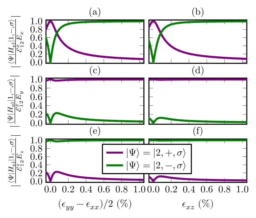
After discussing the interaction with magnetic fields which is essential to split the pseudo-spin levels and for microwave control, we investigating the leading-order electric dipole transition matrix elements in this subsection. These matrix elements are important to characterize the interaction with optical fields. In the absence of strain all leading-order transitions conserve the spin and [42]. For simplicity, we focus on the transitions between the KD and the two KDs under the (leading-order) influence of strain. To this end, we calculate
| (17) | ||||
| (18) |
Similar expressions can be analogously calculated for other transitions. We show in Fig. 5 how the electric dipole transition matrix elements evolve as a function of the -type strain elements and . This figure underlines that there are domains where these types of strain enable multiple simultaneous transitions and that strain can significantly impact the selection rules of the defect. The strongest change of the selection rules visible in Fig. 5 is the complete inversion of dipole coupling strength to the GS via polarized fields between the ES KDs under strain. Combined with the influence on we conclude that the circular polarization selection rules in the absence of strain [45] become linear polarization rules in suitably strained samples. For example, in Fig. 5 it can be seen that the transition becomes primarily susceptible to in the presence of strong strain. We can generalize this by considering that for strong (positive) strain , such that we find
| (19) |
Figure 5 and the above expressions directly show that we can generate an orbital three-level system in the configuration where one GS KD couples to two ES KDs in the presence of strain. Considering the equivalent structure of the two doublets, we infer that an orbital Lambda () system can be created analogously.
Because even in the presence of strain the leading-order transitions conserve the pseudo-spin, the spin-conserving transitions to the ES are cyclic if the pseudo-spins inside the KDs are not mixed. These cycling transitions are used in many platforms for spin readout [56, 57, 58, 59, 60]. Since the coupling to a magnetic field aligned with the crystal axis () is diagonal [see Eq. (16)] the pseudo-spins are pure for such a magnetic field. Therefore, the application of a static magnetic field perfectly aligned with the crystal axis, splitting the spin levels without mixing them, enables spin readout even in the presence of strain.
III.4 Pseudo-spin polarization in a highly strained system
While one possible way to initialize a state is a projective measurement, another approach established in a wide range of platforms is coherent population trapping [61, 62, 63, 64, 7, 12, 13, 14]. This approach relies on a Lambda system, but in the case of the V defect in SiC, all the leading order transitions conserve the pseudo-spin of the KDs. For this reason, different hyperfine interactions of KDs [45], additional fields, or higher-order transition rules are needed to polarize the electron spin. Higher orders can be investigated using a Schrieffer-Wolff transformation, but are not discussed here for simplicity (see App. C for the case with strain, or [42] for the case without strain).
Instead, we briefly outline how the combination of strain and a static magnetic field can be used to set up an optical lambda system. In particular, we propose to combine type strain leading to and a magnetic field in the plane (with non-vanishing components). In this case, the KD’s Zeeman terms [see Eq. (16)] are which is diagonalized by the states
| (20) |
with the corresponding eigenvalues,
| (21) |
and the angles . With this, an optical Lambda system made up by the two GS () and one of the ES becomes feasible. As an example we calculate the electric dipole matrix element between the GS and the ES ,
| (22) |
with the spin-conserving matrix elements according to Eq. (III.3). These selection rules also imply that the corresponding decay processes becomes allowed. Combined, this enables the preparation of a pseudo-spin state of the GS KD in the presence of strain.
The readout of the qubit discussed in the previous section relied on cyclic transitions. To make the transitions highly cyclic on demand after using the system we can target [see Eqs. (III.4) and (III.4)]. This can be achieved either by switching the perpendicular component of the magnetic field on and off (e.g., by changing the relative alignment of the magnetic field) or by modulating the perpendicular -tensor component via the strain [53, 51, 54] (see Fig. 4). Note that the adiabatic modulation can be sped up by shortcut to adiabadicity approaches like counter adiabatic driving [65, 66, 67].
III.5 Hyperfine interaction in strained KDs
After the detailed discussion of the interplay of the electronic structure of TM defects in SiC with strain, we now proceed to the hyperfine structure of the KDs in the presence of strain. The Hamiltonian of the hyperfine interaction [Eqs. (7) and (8)] projected onto the strained KDs [Eq. (15)] is
| (23) |
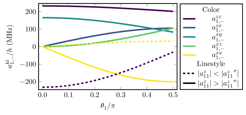
with the hyperfine coupling constants and , , , and . We extract the parameters from the literature values (determined at zero strain) [38, 43, 39, 45] using the following relations by comparing the predicted forms for . The average (quarter of the difference) of between the KDs pertaining to the same doublet yields (). The components and are fully given by and , respectively. We plot the coupling constants of the GS KD as a function of the GS strain mixing angle in Fig. 6, where we assume . Figure 6 shows that due to the symmetry breaking, additional hyperfine elements become non-zero compared with the case of intact symmetry ().
While the magnitudes of the different components of the two GS KDs and the lower ES KD are agreed upon within several works [38, 43, 45, 39, 68] and thereby enabled the independent determination of the relative sign of the lowest ES and GS [40], the relative sign between the KDs of the same doublet does not have this support. Therefore, we show in Fig. 6 two possible configurations, one for opposite signs (here, for ) where the orbital hyperfine dominates the diagonal interaction and one for the same signs (here, ) where the anisotropic hyperfine and Fermi contact interaction are dominant. The vastly different strain dependencies of the strain coupling elements for the different signs shows that by measuring this dependence (for example by using a strong, constant magnetic field) it is possible to determine the relative signs of the hyperfine tensor of the GS KDs without using direct transitions between those. This would then give us insight into whether the or is dominant, where the former stems from the anisotropic and Fermi contact terms and the latter from the orbital angular momentum interacting with the nuclear spin. Therefore, such a measurement would determine which of these interactions is prevalent.
In the previously proposed nuclear spin-polarization protocol [45], unstrained samples were considered. Fundamentally, the different forms of the hyperfine coupling between the KDs were devised to a driven dissipative protocol to polarize the nuclear spin. In this protocol spin-flipping transitions are driven in combination with spin-conserving decays leading to the polarization of nuclear and electronic spin. We expect this protocol to be possible if the () strain is sufficiently small such that the GS are dominated by the hyperfine terms and the ES by the terms . This can be estimated using the strain mixing angles for [see Eq. (15)] and Figs. 6 and 3.
On the other hand, for highly () strained samples, one has a non-negligible . In this case, one can apply a strong magnetic field along the crystal axis to suppress the hyperfine interaction terms . In this case, the quantization axis of the nuclear spin is tilted depending on the KD. This is immediately visible by investigating a single pseudo-spin manifold
| (24) |
with the electronic energy and where the magnetic field along -direction suppresses the off-diagonal terms. By first applying a rotation around the -axis by the angle and then a rotation around the -axis with the angle , we diagonalize this manifold, yielding the diagonal hyperfine term in the rotated basis,
| (25) |
The rotations reflect that the nuclear spin experiences a strain, pseudo-spin, and KD dependent principal axis tilt. Independent of the pseudo spin, it is possible to drive a (pseudo-spin) conserving transition to an ancillary state (AS) with a different principal axis tilt incrementally increasing the nuclear-spin polarization. This enables nuclear polarization. For simplicity, we will discuss an approach based on purely -type strain, i.e. and . Transforming any KDs pseudo-spin manifold into the diagonal basis of the GS KDs down state (), we find that we need to replace in Eq. (25) with the relative axis tilt angle . The relative tilt angle formalizes that driving to the AS conserving the nuclear-spin state will lead to a nuclear spin precession in the AS until the state decays back to the GS.
This interaction of the nuclear-spin eigenstates of the GS in the AS can be used to polarize the nuclear spin. A suitable domain for this may be but where we can approximate the eigenstates of the AS using first-order perturbation theory. The eigenstates of the ancillary KD pseudo-spin (in the principal axis system of the GS KD down state) are
| (26) |
The form of these states shows the possibility to resonantly drive the transitions from the GS state to the corresponding from where the decay mainly occurs to the GS state (if ). Here, the small angle ensures that the main decay does not decrease the nuclear magnetic moment again, while still enabling a resonant drive of the polarizing transition. This process polarizes the nuclear spin stepwise. The outlined approach works with the transition to an ES or the second GS, given that the nuclear transition lines can be resolved. This is in contrast to the proposed zero-strain protocol, where a pseudo-spin flipping transition in combination with the correct polarization renders this requirement unnecessary.
While we focused for concreteness on one additional example including strain in this work, we note that combining our model with the general approach outlined in [45], protocols optimized for different scenarios can be developed that are best matched to the technical setup.
IV Conclusion
We studied the influence of strain on transition-metal defects in SiC, focusing on a particularly promising center for quantum technology applications, the substitutional vanadium defect at the site of 4H-SiC. We found that using strain enables the engineering of the electronic -tensor and optical selection rules, thereby opening the possibility for strain-controlled manipulation (microwave gates) within the KDs, as well as and V optical three-level setups where both branches can be driven using the same polarization. By combining strain and magnetic fields, we showed a path towards engineering systems for the pseudo-spin states of the KD, thus enabling further prospects such as state preparation within the GS KD. We also discussed the prospect of state readout of strained defects using cycling transitions.
Furthermore, we showed the influence of strain on the hyperfine interaction within the KDs. Here, we found that the previously proposed polarization protocol is likely not applicable anymore for strongly strained samples. Therefore, we discussed one example of an application of our theory where it is straightforward to find different polarization schemes even in the presence of strain. A natural next step would be to exploit our theoretical insights in future experiments.
Acknowledgements.
We acknowledge funding from the European Union’s Horizon 2020 research and innovation programme under Grant Agreement No. 862721 (QuanTELCO). B.T. and G.B. additionally acknowledge funding from the German Federal Ministry of Education and Research (BMBF) under the Grant Agreement No. 13N16212 (SPINNING). A.G. acknowledges the support by the National Excellence Program for the project of Quantum-coherent materials (NKFIH Grant No. KKP129866) as well as by the Ministry of Culture and Innovation and the National Research, Development and Innovation Office within the Quantum Information National Laboratory of Hungary (Grant No. 2022-2.1.1-NL-2022-00004). A.G. additionally acknowledges the high-performance computational resources provided by KIFU (Governmental Agency for IT Development) institute of Hungary and the European Commission for the project QuMicro (Grant No. 101046911).Appendix A DFT calculation methods
We model the vanadium defect embedded in a 128-atom 4H-SiC supercell. Its electronic structure is calculated using the plane-wave based Vienna Ab-initio Simulation Package (VASP) [69, 70, 71, 72], with the -point approximation for the k-point sampling. The plane wave cutoff is set to 420 eV and PAW method [73] is used for the core electrons. We apply DFT using the hybrid exchange functional of Heyd, Scuseria, and Ernzerhof (HSE06) [74] with on-site correction (DFT+U) according to the Dudarev-approach [75], where the d-orbitals of the vanadium atom is effected by eV [76]. The atomic configurations are relaxed to forces smaller than 0.01 eV/Å. Excited state electronic configurations are calculated with the constrained occupation -SCF method [77]. The methods for applying strain is discussed in Ref. [46]. We note that the local defect structure is relaxed within the strain constraint applied to the lattice.
The results of this simulation are discussed in the main text and we additionally provided all slopes extracted for the coupling to strain in Tab. 2. In this table takes the same role as [see Eq. (11)] but takes into account that we cannot assume them to be the same a priori within the DFT calculation. We encode the slope of the ES and GS level splitting in by choosing as we discuss in the main text.
| symmetry | parameter | calculated value (eV/strain) |
|---|---|---|
| 1.04(1) | ||
| 0.56(5) | ||
| 0.94(2) | ||
| 0.85(2) | ||
| 1.037(2) | ||
| 0.582(2) | ||
| 0.958(4) | ||
| 0.84(1) | ||
| 1.9(1) | ||
| 1.26(8) |
Appendix B Crystal field eigenstates and signs of the strain coupling constants
Inside the orbital projections the crystal eigenstates are given as
| (27) | ||||
where the crystal mixing angle describes the admixture of states that transform equally under .
In the absence of spin-orbit coupling the doublet states split due to -strain, we use this to determine the sign of the strain coupling constants. The eigenvectors for purely strain are (within the doublet projection) given by
| (28) | ||||
| (29) |
with the eigenvalues . We note the parallel of these pairs of states to the cubic harmonics , , , , and . With this we find that the strain eigenstates are proportional to the distinct sets of cubic harmonics and .
With this we can obtain the sign of the coupling from the DFT simulation without spin by comparing the projection on the cubic harmonics (of the -orbital). We find that for in the GS (ES) the lower energy state is mainly (), i.e. the () state, such that (). Analogously, for in the GS (ES) the lower energy state is mainly (), i.e. the () state, such that ().
Due to the known transformation properties of the states from the literature (using the difference in the hyperfine tensor) we assign the lower KD of the GS in the absence of strain to and in the ES to [38, 43, 45, 39, 40]. To accommodate this in the model, we use that for the vanadium defect in the site in 4H-SiC, and .
Appendix C Higher-order effects
To understand higher order effects we treat a purely -type strain using a Schrieffer-Wolff transformation [78]. To this end, we perturbatively take block off-diagonal elements of the spin-orbit and strain Hamiltonians (together) into account. We do the following calculations in the basis where the leading-order doublet Hamiltonians given in Eq. (15) are diagonalized, such that we can afterwards directly study the corrections affecting the KDs. Then we use the transformation and, within first-order perturbation theory,
| (30) |
where we directly neglect spin-orbit and strain terms in the denominator as they are part of the higher (neglected) orders. The corrections to the zero-field energies are then given by which is block-diagonal in the KDs and corrects their energies by
| (31) | ||||
| (32) | ||||
| (33) |
where .
In addition to this, the corresponding corrections of the remaining parts of the full Hamiltonian can be calculated as . For instance this corrects the coupling to a magnetic field along the crystal axis projected onto the KDs as
| (34) | ||||
| (35) | ||||
| (36) |
where one can neglect the off-diagonal matrix elements considering that they are suppressed by the leading-order term , as we expect for . While in this article we focus on providing the straight-forward recipe to calculate higher-order terms for simplicity, previous work takes higher-order effects in the spin-orbit coupling only (without strain) into account [42, 43, 45]. Analogously, expressions for other magnetic-field directions and parts of the Hamiltonian can be calculated using but are omitted here.
References
- Aharonovich et al. [2016] I. Aharonovich, D. Englund, and M. Toth, Solid-state single-photon emitters, Nat. Photonics 10, 631 (2016).
- Heshami et al. [2016] K. Heshami, D. G. England, P. C. Humphreys, P. J. Bustard, V. M. Acosta, J. Nunn, and B. J. Sussman, Quantum memories: emerging applications and recent advances, J. Mod. Opt. 63, 2005 (2016).
- Awschalom et al. [2021] D. Awschalom, K. K. Berggren, H. Bernien, S. Bhave, L. D. Carr, P. Davids, S. E. Economou, D. Englund, A. Faraon, M. Fejer, S. Guha, M. V. Gustafsson, E. Hu, L. Jiang, J. Kim, B. Korzh, P. Kumar, P. G. Kwiat, M. Lončar, M. D. Lukin, D. A. Miller, C. Monroe, S. W. Nam, P. Narang, J. S. Orcutt, M. G. Raymer, A. H. Safavi-Naeini, M. Spiropulu, K. Srinivasan, S. Sun, J. Vučković, E. Waks, R. Walsworth, A. M. Weiner, and Z. Zhang, Development of quantum interconnects (quics) for next-generation information technologies, PRX Quantum 2, 017002 (2021).
- He et al. [1993] X.-F. He, N. B. Manson, and P. T. H. Fisk, Paramagnetic resonance of photoexcited N-V defects in diamond. I. level anticrossing in the 3A ground state, Phys. Rev. B 47, 8809 (1993).
- Gaebel et al. [2006] T. Gaebel, M. Domhan, I. Popa, C. Wittmann, P. Neumann, F. Jelezko, J. R. Rabeau, N. Stavrias, A. D. Greentree, S. Prawer, J. Meijer, J. Twamley, P. R. Hemmer, and J. Wrachtrup, Room-temperature coherent coupling of single spins in diamond, Nature Phys. 2, 408 (2006).
- Childress et al. [2006] L. Childress, M. V. G. Dutt, J. M. Taylor, A. S. Zibrov, F. Jelezko, J. Wrachtrup, P. R. Hemmer, and M. D. Lukin, Coherent dynamics of coupled electron and nuclear spin qubits in diamond, Science 314, 281 (2006).
- Santori et al. [2006] C. Santori, P. Tamarat, P. Neumann, J. Wrachtrup, D. Fattal, R. G. Beausoleil, J. Rabeau, P. Olivero, A. D. Greentree, S. Prawer, F. Jelezko, and P. Hemmer, Coherent population trapping of single spins in diamond under optical excitation, Phys. Rev. Lett. 97, 247401 (2006).
- Gali et al. [2008] A. Gali, M. Fyta, and E. Kaxiras, Ab initio supercell calculations on nitrogen-vacancy center in diamond: Electronic structure and hyperfine tensors, Phys. Rev. B 77, 155206 (2008).
- Felton et al. [2009] S. Felton, A. M. Edmonds, M. E. Newton, P. M. Martineau, D. Fisher, D. J. Twitchen, and J. M. Baker, Hyperfine interaction in the ground state of the negatively charged nitrogen vacancy center in diamond, Phys. Rev. B 79, 075203 (2009).
- Maze et al. [2011] J. R. Maze, A. Gali, E. Togan, Y. Chu, A. Trifonov, E. Kaxiras, and M. D. Lukin, Properties of nitrogen-vacancy centers in diamond: the group theoretic approach, New J. Phys. 13, 025025 (2011).
- Fuchs et al. [2011] G. D. Fuchs, G. Burkard, P. V. Klimov, and D. D. Awschalom, A quantum memory intrinsic to single nitrogen–vacancy centres in diamond, Nature Phys. 7, 789 (2011).
- Togan et al. [2011] E. Togan, Y. Chu, A. Imamoglu, and M. D. Lukin, Laser cooling and real-time measurement of the nuclear spin environment of a solid-state qubit, Nature 478, 497 (2011).
- Yale et al. [2013] C. G. Yale, B. B. Buckley, D. J. Christle, G. Burkard, F. J. Heremans, L. C. Bassett, and D. D. Awschalom, All-optical control of a solid-state spin using coherent dark states, Proceedings of the National Academy of Sciences 110, 7595 (2013).
- Golter et al. [2013] D. A. Golter, K. N. Dinyari, and H. Wang, Nuclear-spin-dependent coherent population trapping of single nitrogen-vacancy centers in diamond, Phys. Rev. A 87, 035801 (2013).
- Busaite et al. [2020] L. Busaite, R. Lazda, A. Berzins, M. Auzinsh, R. Ferber, and F. Gahbauer, Dynamic 14N nuclear spin polarization in nitrogen-vacancy centers in diamond, Phys. Rev. B 102, 224101 (2020).
- Hegde et al. [2020] S. S. Hegde, J. Zhang, and D. Suter, Efficient quantum gates for individual nuclear spin qubits by indirect control, Phys. Rev. Lett. 124, 220501 (2020).
- Doherty et al. [2013] M. W. Doherty, N. B. Manson, P. Delaney, F. Jelezko, J. Wrachtrup, and L. C. L. Hollenberg, The nitrogen-vacancy colour centre in diamond, Phys. Rep. 528, 1 (2013).
- Suter and Jelezko [2017] D. Suter and F. Jelezko, Single-spin magnetic resonance in the nitrogen-vacancy center of diamond, Prog. Nucl. Magn. Reson. Spectrosc. 98-99, 50 (2017).
- Pezzagna and Meijer [2021] S. Pezzagna and J. Meijer, Quantum computer based on color centers in diamond, Applied Physics Reviews 8, 011308 (2021).
- Thiering and Gali [2018] G. Thiering and A. Gali, Theory of the optical spin-polarization loop of the nitrogen-vacancy center in diamond, Phys. Rev. B 98, 085207 (2018).
- Gruber et al. [1997] A. Gruber, A. Dräbenstedt, C. Tietz, L. Fleury, J. Wrachtrup, and C. von Borczyskowski, Scanning confocal optical microscopy and magnetic resonance on single defect centers, Science 276, 2012 (1997), https://www.science.org/doi/pdf/10.1126/science.276.5321.2012 .
- Wellmann [2018] P. J. Wellmann, Review of SiC crystal growth technology, Semiconductor Science and Technology 33, 103001 (2018).
- Liu et al. [2020] J. Liu, Z. Xu, Y. Song, H. Wang, B. Dong, S. Li, J. Ren, Q. Li, M. Rommel, X. Gu, B. Liu, M. Hu, and F. Fang, Confocal photoluminescence characterization of silicon-vacancy color centers in 4H-SiC fabricated by a femtosecond laser, Nanotechnology and Precision Engineering (NPE) 3, 218 (2020), https://pubs.aip.org/tu/npe/article-pdf/3/4/218/16662950/218_1_online.pdf .
- Chakravorty et al. [2021] A. Chakravorty, B. Singh, H. Jatav, R. Meena, D. Kanjilal, and D. Kabiraj, Controlled generation of photoemissive defects in 4H-SiC using swift heavy ion irradiation, Journal of Applied Physics 129, 245905 (2021), https://pubs.aip.org/aip/jap/article-pdf/doi/10.1063/5.0051328/15268515/245905_1_online.pdf .
- Song et al. [2019] B.-S. Song, T. Asano, S. Jeon, H. Kim, C. Chen, D. D. Kang, and S. Noda, Ultrahigh-Q photonic crystal nanocavities based on 4H silicon carbide, Optica 6, 991 (2019).
- Lukin et al. [2020] D. M. Lukin, C. Dory, M. A. Guidry, K. Y. Yang, S. D. Mishra, R. Trivedi, M. Radulaski, S. Sun, D. Vercruysse, G. H. Ahn, and J. Vučković, 4H-silicon-carbide-on-insulator for integrated quantum and nonlinear photonics, Nature Photonics 14, 330 (2020).
- Guidry et al. [2020] M. A. Guidry, K. Y. Yang, D. M. Lukin, A. Markosyan, J. Yang, M. M. Fejer, and J. Vučković, Optical parametric oscillation in silicon carbide nanophotonics, Optica 7, 1139 (2020).
- Radulaski et al. [2017] M. Radulaski, M. Widmann, M. Niethammer, J. L. Zhang, S.-Y. Lee, T. Rendler, K. G. Lagoudakis, N. T. Son, E. Janzén, T. Ohshima, J. Wrachtrup, and J. Vučković, Scalable quantum photonics with single color centers in silicon carbide, Nano Letters 17, 1782 (2017), pMID: 28225630, https://doi.org/10.1021/acs.nanolett.6b05102 .
- Wang et al. [2017] J. Wang, Y. Zhou, X. Zhang, F. Liu, Y. Li, K. Li, Z. Liu, G. Wang, and W. Gao, Efficient generation of an array of single silicon-vacancy defects in silicon carbide, Phys. Rev. Appl. 7, 064021 (2017).
- Sörman et al. [2000] E. Sörman, N. T. Son, W. M. Chen, O. Kordina, C. Hallin, and E. Janzén, Silicon vacancy related defect in 4H and 6H SiC, Phys. Rev. B 61, 2613 (2000).
- Janzén et al. [2009] E. Janzén, A. Gali, P. Carlsson, A. Gällström, B. Magnusson, and N. Son, The silicon vacancy in SiC, Physica B: Condensed Matter 404, 4354 (2009).
- Nagy et al. [2018] R. Nagy, M. Widmann, M. Niethammer, D. B. R. Dasari, I. Gerhardt, O. O. Soykal, M. Radulaski, T. Ohshima, J. Vučković, N. T. Son, I. G. Ivanov, S. E. Economou, C. Bonato, S.-Y. Lee, and J. Wrachtrup, Quantum properties of dichroic silicon vacancies in silicon carbide, Phys. Rev. Appl. 9, 034022 (2018).
- Gali et al. [2010] A. Gali, A. Gällström, N. T. Son, and E. Janzén, Theory of neutral divacancy in sic: A defect for spintronics, in Silicon Carbide and Related Materials 2009, Materials Science Forum, Vol. 645 (Trans Tech Publications Ltd, 2010) pp. 395–397.
- Falk et al. [2013] A. L. Falk, B. B. Buckley, G. Calusine, W. F. Koehl, V. V. Dobrovitski, A. Politi, C. A. Zorman, P. X.-L. Feng, and D. D. Awschalom, Polytype control of spin qubits in silicon carbide, Nature Communications 4, 1819 (2013).
- Bosma et al. [2018] T. Bosma, G. J. J. Lof, C. M. Gilardoni, O. V. Zwier, F. Hendriks, B. Magnusson, A. Ellison, A. Gällström, I. G. Ivanov, N. T. Son, R. W. A. Havenith, and C. H. van der Wal, Identification and tunable optical coherent control of transition-metal spins in silicon carbide, npj Quantum Inf. 4, 48 (2018).
- Spindlberger et al. [2019] L. Spindlberger, A. Csóré, G. Thiering, S. Putz, R. Karhu, J. Hassan, N. Son, T. Fromherz, A. Gali, and M. Trupke, Optical properties of vanadium in 4H silicon carbide for quantum technology, Phys. Rev. Appl. 12, 014015 (2019).
- Gilardoni et al. [2020] C. M. Gilardoni, T. Bosma, D. van Hien, F. Hendriks, B. Magnusson, A. Ellison, I. G. Ivanov, N. T. Son, and C. H. van der Wal, Spin-relaxation times exceeding seconds for color centers with strong spin–orbit coupling in SiC, New J. Phys. 22, 103051 (2020).
- Wolfowicz et al. [2020] G. Wolfowicz, C. P. Anderson, B. Diler, O. G. Poluektov, F. J. Heremans, and D. D. Awschalom, Vanadium spin qubits as telecom quantum emitters in silicon carbide, Sci. Adv. 6, eaaz1192 (2020).
- Astner et al. [2022] T. Astner, P. Koller, C. M. Gilardoni, J. Hendriks, N. T. Son, I. G. Ivanov, J. U. Hassan, C. H. v. d. Wal, and M. Trupke, Vanadium in silicon carbide: Telecom-ready spin centres with long relaxation lifetimes and hyperfine-resolved optical transitions, arXiv (2022), arXiv:2206.06240 [quant-ph] .
- Cilibrizzi et al. [2023] P. Cilibrizzi, M. J. Arshad, B. Tissot, N. T. Son, I. G. Ivanov, T. Astner, P. Koller, M. Ghezellou, J. Ul-Hassan, D. White, C. Bekker, G. Burkard, M. Trupke, and C. Bonato, Ultra-narrow inhomogeneous spectral distribution of telecom-wavelength vanadium centres in isotopically-enriched silicon carbide, arXiv 10.48550/ARXIV.2305.01757 (2023), arXiv:2206.06240 [quant-ph] .
- Csóré and Gali [2020] A. Csóré and A. Gali, Ab initio determination of pseudospin for paramagnetic defects in SiC, Phys. Rev. B 102, 241201 (2020).
- Tissot and Burkard [2021a] B. Tissot and G. Burkard, Spin structure and resonant driving of spin-1/2 defects in SiC, Phys. Rev. B 103, 064106 (2021a).
- Tissot and Burkard [2021b] B. Tissot and G. Burkard, Hyperfine structure of transition metal defects in SiC, Phys. Rev. B 104, 064102 (2021b).
- Gilardoni et al. [2021] C. M. Gilardoni, I. Ion, F. Hendriks, M. Trupke, and C. H. van der Wal, Hyperfine-mediated transitions between electronic spin-1/2 levels of transition metal defects in SiC, New J. Phys. 10.1088/1367-2630/ac1641 (2021).
- Tissot et al. [2022] B. Tissot, M. Trupke, P. Koller, T. Astner, and G. Burkard, Nuclear spin quantum memory in silicon carbide, Phys. Rev. Res. 4, 033107 (2022).
- Udvarhelyi et al. [2018] P. Udvarhelyi, V. O. Shkolnikov, A. Gali, G. Burkard, and A. Pályi, Spin-strain interaction in nitrogen-vacancy centers in diamond, Phys. Rev. B 98, 075201 (2018).
- Udvarhelyi and Gali [2018] P. Udvarhelyi and A. Gali, Ab initio spin-strain coupling parameters of divacancy qubits in silicon carbide, Phys. Rev. Appl. 10, 054010 (2018).
- Udvarhelyi et al. [2020] P. Udvarhelyi, G. Thiering, N. Morioka, C. Babin, F. Kaiser, D. Lukin, T. Ohshima, J. Ul-Hassan, N. T. Son, J. Vučković, J. Wrachtrup, and A. Gali, Vibronic states and their effect on the temperature and strain dependence of silicon-vacancy qubits in 4H-SiC, Phys. Rev. Appl. 13, 054017 (2020).
- Udvarhelyi et al. [2023] P. Udvarhelyi, T. Clua-Provost, A. Durand, J. Li, J. H. Edgar, B. Gil, G. Cassabois, V. Jacques, and A. Gali, A planar defect spin sensor in a two-dimensional material susceptible to strain and electric fields (2023), arXiv:2304.00492 [quant-ph] .
- Koppenhöfer et al. [2023] M. Koppenhöfer, C. Padgett, J. V. Cady, V. Dharod, H. Oh, A. C. B. Jayich, and A. A. Clerk, Single-spin readout and quantum sensing using optomechanically induced transparency, Phys. Rev. Lett. 130, 093603 (2023).
- Meesala et al. [2018] S. Meesala, Y.-I. Sohn, B. Pingault, L. Shao, H. A. Atikian, J. Holzgrafe, M. Gündoğan, C. Stavrakas, A. Sipahigil, C. Chia, R. Evans, M. J. Burek, M. Zhang, L. Wu, J. L. Pacheco, J. Abraham, E. Bielejec, M. D. Lukin, M. Atatüre, and M. Lončar, Strain engineering of the silicon-vacancy center in diamond, Physical Review B 97, 205444 (2018).
- Nguyen et al. [2019] C. T. Nguyen, D. D. Sukachev, M. K. Bhaskar, B. Machielse, D. S. Levonian, E. N. Knall, P. Stroganov, C. Chia, M. J. Burek, R. Riedinger, H. Park, M. Lončar, and M. D. Lukin, An integrated nanophotonic quantum register based on silicon-vacancy spins in diamond, Physical Review B 100, 165428 (2019).
- Ovartchaiyapong et al. [2014] P. Ovartchaiyapong, K. W. Lee, B. A. Myers, and A. C. B. Jayich, Dynamic strain-mediated coupling of a single diamond spin to a mechanical resonator, Nature Communications 5, 4429 (2014).
- Barfuss et al. [2019] A. Barfuss, M. Kasperczyk, J. Kölbl, and P. Maletinsky, Spin-stress and spin-strain coupling in diamond-based hybrid spin oscillator systems, Physical Review B 99, 174102 (2019).
- Note [1] According to previous DFT results the site corresponds to the configuration of vanadium in 4H-SiC [41].
- Robledo et al. [2011] L. Robledo, L. Childress, H. Bernien, B. Hensen, P. F. A. Alkemade, and R. Hanson, High-fidelity projective read-out of a solid-state spin quantum register, Nature 477, 574 (2011).
- Delteil et al. [2014] A. Delteil, W. Gao, P. Fallahi, J. Miguel-Sanchez, and A. Imamoğlu, Observation of quantum jumps of a single quantum dot spin using submicrosecond single-shot optical readout, Phys. Rev. Lett. 112, 116802 (2014).
- Sukachev et al. [2017] D. D. Sukachev, A. Sipahigil, C. T. Nguyen, M. K. Bhaskar, R. E. Evans, F. Jelezko, and M. D. Lukin, Silicon-vacancy spin qubit in diamond: a quantum memory exceeding 10 ms with single-shot state readout, Phys. Rev. Lett. 119, 223602 (2017).
- Raha et al. [2020] M. Raha, S. Chen, C. M. Phenicie, S. Ourari, A. M. Dibos, and J. D. Thompson, Optical quantum nondemolition measurement of a single rare earth ion qubit, Nat. Commun. 11, 1605 (2020).
- Appel et al. [2021] M. H. Appel, A. Tiranov, A. Javadi, M. C. Löbl, Y. Wang, S. Scholz, A. D. Wieck, A. Ludwig, R. J. Warburton, and P. Lodahl, Coherent spin-photon interface with waveguide induced cycling transitions, Phys. Rev. Lett. 126, 013602 (2021).
- Gray et al. [1978] H. R. Gray, R. M. Whitley, and C. R. Stroud, Coherent trapping of atomic populations, Opt. Lett. 3, 218 (1978).
- Xu et al. [2008] X. Xu, B. Sun, P. R. Berman, D. G. Steel, A. S. Bracker, D. Gammon, and L. J. Sham, Coherent population trapping of an electron spin in a single negatively charged quantum dot, Nature Phys. 4, 692 (2008).
- Kelly et al. [2010] W. R. Kelly, Z. Dutton, J. Schlafer, B. Mookerji, T. A. Ohki, J. S. Kline, and D. P. Pappas, Direct observation of coherent population trapping in a superconducting artificial atom, Phys. Rev. Lett. 104, 163601 (2010).
- Dong et al. [2012] C. Dong, V. Fiore, M. C. Kuzyk, and H. Wang, Optomechanical dark mode, Science 338, 1609 (2012).
- Demirplak and Rice [2003] M. Demirplak and S. A. Rice, Adiabatic population transfer with control fields, J. Phys. Chem. A 107, 9937 (2003).
- Berry [2009] M. V. Berry, Transitionless quantum driving, J. Phys. A: Math. Theor. 42, 365303 (2009).
- Guéry-Odelin et al. [2019] D. Guéry-Odelin, A. Ruschhaupt, A. Kiely, E. Torrontegui, S. Martínez-Garaot, and J. G. Muga, Shortcuts to adiabaticity: Concepts, methods, and applications, Rev. Mod. Phys. 91, 045001 (2019).
- Hendriks et al. [2022] J. Hendriks, C. M. Gilardoni, C. Adambukulam, A. Laucht, and C. H. v. d. Wal, Coherent spin dynamics of hyperfine-coupled vanadium impurities in silicon carbide, CoRR (2022), arXiv:2210.09942 [quant-ph] .
- Kresse and Hafner [1993] G. Kresse and J. Hafner, Ab initio molecular dynamics for liquid metals, Phys. Rev. B 47, 558 (1993).
- Kresse and Furthmüller [1996a] G. Kresse and J. Furthmüller, Efficient iterative schemes for ab initio total-energy calculations using a plane-wave basis set, Phys. Rev. B 54, 11169 (1996a).
- Kresse and Furthmüller [1996b] G. Kresse and J. Furthmüller, Efficiency of ab-initio total energy calculations for metals and semiconductors using a plane-wave basis set, Comput. Mater. Sci. 6, 15 (1996b).
- Paier et al. [2006] J. Paier, M. Marsman, K. Hummer, G. Kresse, I. C. Gerber, and J. G. Ángyán, Screened hybrid density functionals applied to solids, J. Chem. Phys. 124, 154709 (2006).
- Blöchl [1994] P. E. Blöchl, Projector augmented-wave method, Phys. Rev. B 50, 17953 (1994).
- Krukau et al. [2006] A. V. Krukau, O. A. Vydrov, A. F. Izmaylov, and G. E. Scuseria, Influence of the exchange screening parameter on the performance of screened hybrid functionals, J. Chem. Phys. 125, 224106 (2006).
- Dudarev et al. [1998] S. L. Dudarev, G. A. Botton, S. Y. Savrasov, C. J. Humphreys, and A. P. Sutton, Electron-energy-loss spectra and the structural stability of nickel oxide: An LSDA+U study, Phys. Rev. B 57, 1505 (1998).
- Ivády et al. [2013] V. Ivády, I. A. Abrikosov, E. Janzén, and A. Gali, Role of screening in the density functional applied to transition-metal defects in semiconductors, Phys. Rev. B 87, 205201 (2013).
- Gali et al. [2009] A. Gali, E. Janzén, P. Deák, G. Kresse, and E. Kaxiras, Theory of spin-conserving excitation of the NV- center in diamond, Phys. Rev. Lett. 103, 186404 (2009).
- Bravyi et al. [2011] S. Bravyi, D. P. DiVincenzo, and D. Loss, Schrieffer-Wolff transformation for quantum many-body systems, Ann. Phys. 326, 2793 (2011).