Isolating the Nonlinear Optical Response of a \ceMoS2 Monolayer under Extreme Screening of a Metal Substrate
Abstract
Transition metal dichalcogenides (TMDCs) monolayers, as two-dimensional (2D) direct bandgap semiconductors, hold promise for advanced optoelectronic and photocatalytic devices. Interaction with three-dimensional (3D) metals, like Au, profoundly affects their optical properties, posing challenges in characterizing the monolayer’s optical responses within the semiconductor-metal junction. In this study, using precise polarization-controlled final-state sum frequency generation (FS-SFG), we successfully isolated the optical responses of a \ceMoS2 monolayer from a \ceMoS2/Au junction. The resulting SFG spectra exhibit a linear lineshape, devoid of A or B exciton features, attributed to the strong dielectric screening and substrate induced doping. The linear lineshape illustrates the expected constant density of states (DOS) at the band edge of the 2D semiconductor, a feature often obscured by excitonic interactions in week-screening conditions such as in a free-standing monolayer. Extrapolation yields the onset of a direct quasiparticle bandgap of about eV, indicating a strong bandgap renormalization. This study not only enriches our understanding of the optical responses of a 2D semiconductor in extreme screening conditions but also provides a critical reference for advancing 2D semiconductor-based photocatalytic applications.
I Introduction
The unique appeal of monolayers of transition metal dichalcogenides (TMDCs) lies in their distinctive characteristics as two-dimensional (2D) direct bandgap semiconductors [1, 2]. The strong light-matter interaction and the quantum confinement effect position these materials as promising candidates for advancing next-generation optoelectronic and photocatalytic devices [3, 4, 5, 6]. In light of these prospects, a fundamental question arises: How does a 2D TMDC monolayer maintain its semiconductor characteristics when interfaced with a three-dimensional (3D) metal? This query is pivotal, considering the well-known strong screening and doping effects associated with bulk metals. Beyond its fundamental implications, this question also holds practical relevance within the fields of TMDC-based 2D transistors [7, 8, 9] and photocatalysis [10, 11, 12]. However, the precise characterization of the electronic properties of a 2D semiconductor on a 3D metal substrate presents substantial challenges. Techniques such as scanning tunneling spectroscopy (STS) offer a means of gauging the electronic bandgap by monitoring the onset of tunneling current [13, 14]. However, accurately determining the onset of tunneling current remains a non-trivial task, potentially introducing ambiguity in the derived bandgap energy [15]. An alternative approach involving time- and angle-resolved photoemission spectroscopy (tr-ARPES) shows promise for electronic bandgap determination [16, 17]. However, the applicability of tr-ARPES is constrained by its demanding experimental requisites.
There is a well-established optical method in the device community, the Tauc plot, which has been used extensively to straightforwardly determine the bandgap of 3D amorphous semiconductors [18, 19, 20]. While this method may also be adapted for use with crystalline semiconductors such as thin layers of TMDCs after certain modifications, challenges arise due to the presence of excitonic features at the band edge. There is an ongoing debate regarding the construction of the Tauc plot for TMDC systems. Some studies involve drawing the slope from the lower-energy side of the A exciton [21, 22], while others base it on the quasiparticle bandgap [23, 24] and simply ignore the excitonic features. Clearly, the accurate characterization of the onset of the band edge of a TMDC monolayer depends on a comprehensive understanding of its optical properties under different environments.
Theoretically, a 2D semiconductor with direct bandgap is expected to have a constant density of states (DOS) at the band edges within a quasi-particle picture [20]. The optical response, which is directly related to the joint DOS, should ideally have a linear lineshape due to the convolution of two constant functions. However, in most practical TMDC systems, the insufficient screening generally enhances the Coulomb interaction between the electrons and holes, leading to exciton formation and complicating the lineshapes. Intriguingly, by placing the TMDC on a metal surface, it may be possible to recover the intrinsic exciton-free optical response of the 2D material. In this case, it is possible to extract the onset of the band edge from the linear extrapolation, analogous to the Tauc plot. Regrettably, when the TMDC is positioned on a metal surface, it is extremely difficult to isolate its pure optical response from that of the underlying metallic substrate. For instance, in the case of a \ceMoS2 monolayer on Au, the photoluminescence (PL) signal is completely quenched [25, 26]. While absorption or reflectivity measurements can still provide an optical response from the TMDC monolayer on a metal system, the extensive optical response from the free electron of the substrate often obscures minor exciton features [27], even though some subtle features in the first derivative of the spectrum have been reported [28]. These persistent challenges impede a comprehensive understanding of the optical behavior of TMDC monolayers interfaced with a metal substrate.
Sum frequency generation spectroscopy, a second-order nonlinear spectroscopic technique[29, 30], offers sensitivity to the structural symmetry of \ceMoS2. In a prior study, we demonstrated the possibility of isolating the optical response of \ceMoS2 from that of the metal by leveraging their respective symmetries [31]. In this work, we extensively investigate the influence of a metallic substrate on the spectra of \ceMoS2. For the first time, a linear optical lineshape of the TMDC monolayer has been recovered at the band edge. This not only allows us to unambiguously conclude that the commonly observed A and B excitons disappear under such extreme screening and doping conditions, but also provides previously unrevealed information to discuss the unique electronic property of the TMDC monolayer in contact with metal with the help of density functional theory (DFT) calculations. Given the disappearance of the exciton features, we can derive an analogous Tauc plot method using the pure second-order nonlinear susceptibility () of \ceMoS2. With this method, we succeed in extracting the intrinsic bandgap ( eV) of \ceMoS2 within the semiconductor-metal junction. Many interesting properties of the system are discussed, such as bandgap renormalization, quantum confinement, and light-matter interaction. This study can be extended to other 2D semiconductor and 3D metal junctions which are commonly encountered in optoelectronic and photocatalytic devices. The information obtained can greatly improve our understanding of the optical properties of 2D semiconductors, especially in the presence of significant concentrations of free carriers.
II Results and Discussion
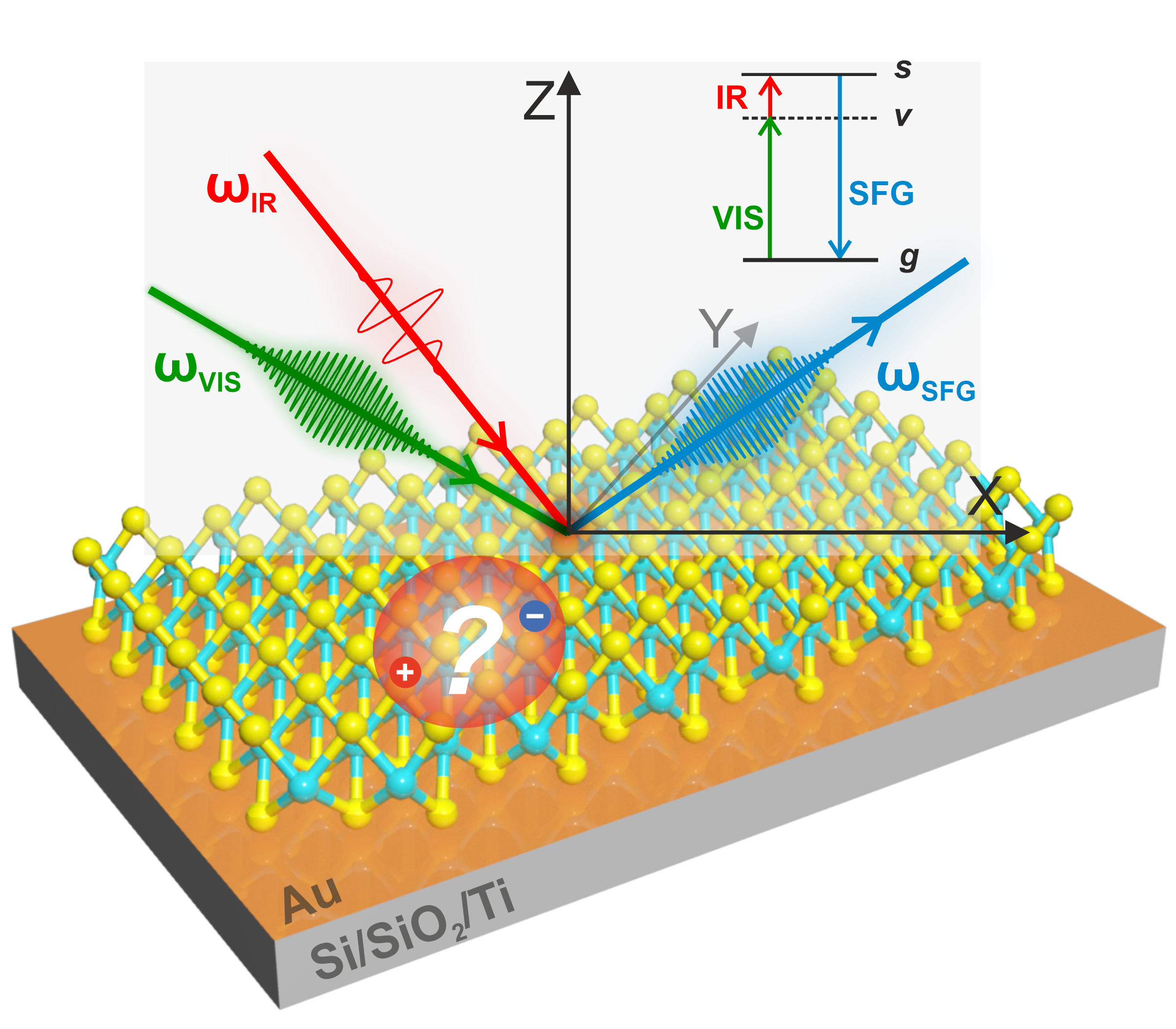
In this study, we collected final-state sum frequency generation (FS-SFG) signals from a monolayer of \ceMoS2 on Au, where the Au film was deposited via physical vapor deposition (PVD). The \ceMoS2/Au sample was prepared through mechanical exfoliation of \ceMoS2 onto a freshly prepared Au surface [26]. For comparative analysis, we also investigated a monolayer of \ceMoS2 on \ceSiO2. Optical images of \ceMoS2/Au and \ceMoS2/\ceSiO2 can be referenced in Fig. S1 within the Supplementary Material [[SeeSupplementalMaterialat[URLwillbeinsertedbypublisher]forexperimentalandtheoreticalinformation, whichincludestheopticalimagesofthesamples, normalizedSFGspectraofPVDAuand\ceMoS2/\ceSiO2, detailsaboutsamplepreparationandlasersetup, DFT-calculatedbandstructureanddensityofstatesof\ceMoS2monolayeronAu.Furthermore, justificationofusing$|χ^(2)|$tocharacterizethebandedge]Yang_spectrum_2023]. A detailed depiction of the SFG experimental setup is provided in Fig. 1. Two laser beams were spatially and temporally overlapped on the sample surface, and the resulting emitted sum frequency photons were detected. The visible beam’s photon energy was centered at 1.56 eV, while the photon energy of infrared (IR) beam was tuned from 0.28-0.41 eV, ensuring that the final-state resonant SFG photon energies covered the A and B exciton energies. The visible beam energy was set at 0.8 J/pulse, and the infrared beam was maintained below 1.0 J/pulse. Both beams were propagated coplanarly with incident angles of 64∘ and 46∘ for the visible and infrared beams, respectively. The polarization of the three beams was individually set to p or s to obtain different polarization combinations, allowing us to choose the one best suited for the intended experiment. During measurements, azimuthal-dependent patterns were initially obtained to guide the collection of FS-SFG spectra at specific azimuthal angles, e.g. the angle with maximum intensity. A -cut alpha quartz was used to obtain a reference signal for the purpose of correcting the frequency-dependent IR intensity. All experiments were conducted under ambient conditions at C. Further details regarding the sample preparation and characterization and the laser setup can be found in our previous work [26, 33, 34] and Supplemental Material [32].
To gain a basic overview of our samples, we initiated our study with Raman and PL measurements. As depicted in Fig. 2, both Raman and PL spectra of \ceMoS2 monolayers on Au and \ceSiO2 substrates manifest pronounced distinctions. Specifically, the Raman spectrum of the \ceMoS2 monolayer on \ceSiO2, as illustrated in Fig. 2(a), exhibits two notable peaks centered at 388.5 cm-1 for the out-of-plane mode and 407.8 cm-1 for the in-plane mode, respectively. The discernible 19.3 cm-1 difference between these modes is characteristic of a monolayer structure [35]. However, the Raman spectrum of \ceMoS2 on Au showcases markedly disparate features. The mode undergoes a redshift to 377.9 cm-1, and the mode exhibits a red shift and splits into two distinct peaks at 396.2 and 403.6 cm-1. These notable changes align with earlier observations [36, 26] and can be attributed to the considerable tensile strain induced by the Au substrate owing to the high-quality contact [26, 37].
The substantial interaction observed at the semiconductor-metal interface is further corroborated by the PL spectrum depicted in Fig. 2(b). The \ceMoS2 sample on \ceSiO2 exhibits distinctive features at 1.81 and 1.97 eV, corresponding to the A and B excitons of \ceMoS2, respectively. The presence of two excitons, A and B, originates from the splitting of the valence band maxima at the K-point, induced by spin-orbit coupling [38]. In stark contrast, the PL signal from the \ceMoS2/Au sample is completely quenched. These optical spectra observations align with previous studies [39, 36, 26]. PL quenching has been reported previously [25] and was understood as the transfer of the photoexcited electron from the conduction band of \ceMoS2 to the Au substrate instead of undergoing radiation relaxation. This hypothesis is supported by tr-ARPES results, which demonstrate ultrafast dynamics of the photoexcited free carriers [16]. However, the behavior of excitons within this heterointerface remained unclear. While there are reports claiming that the A and B excitons remain observable for \ceMoS2 on Au [28], others suggest a conclusion to the contrary [27]. The reason for the dispute is the weak signal of \ceMoS2, which is always hidden under the strong background signal of the Au substrate, making it difficult to unambiguously distinguish between them. Fortunately, second-order nonlinear spectroscopy techniques, such as FS-SFG, provide a unique opportunity to isolate the contribution of the monolayer semiconductor from that of the bulk substrate, capitalizing on their distinct symmetries. Further details regarding this isolation technique are elaborated below.
As demonstrated in earlier studies utilizing single-beam second harmonic generation (SHG), the 2H-\ceMoS2 monolayer is categorized under the point group, displaying a consistent six-fold symmetric pattern of SHG intensity [40, 41, 42]. Our recent investigation using SFG aligns with these prior findings and extends the understanding by revealing that the symmetric pattern of the \ceMoS2 monolayer on Au is highly dependent on polarization, resulting in a lowering of the symmetry to [31]. Within the point group, specific polarization combinations (e.g. spp, pps, psp, and sss, where spp indicates s polarized SFG, p polarized visible, and p polarized infrared beams) yield signals arising from only one azimuthal-dependent second-order susceptibility component inherited from \ceMoS2. By carefully selecting the appropriate polarization combination, SFG enables selective investigation of the \ceMoS2 monolayer and provides the pure response from the \ceMoS2 monolayer free from perturbations by the Au optical response.
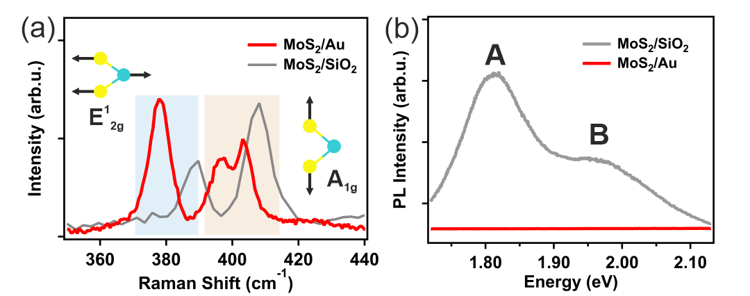
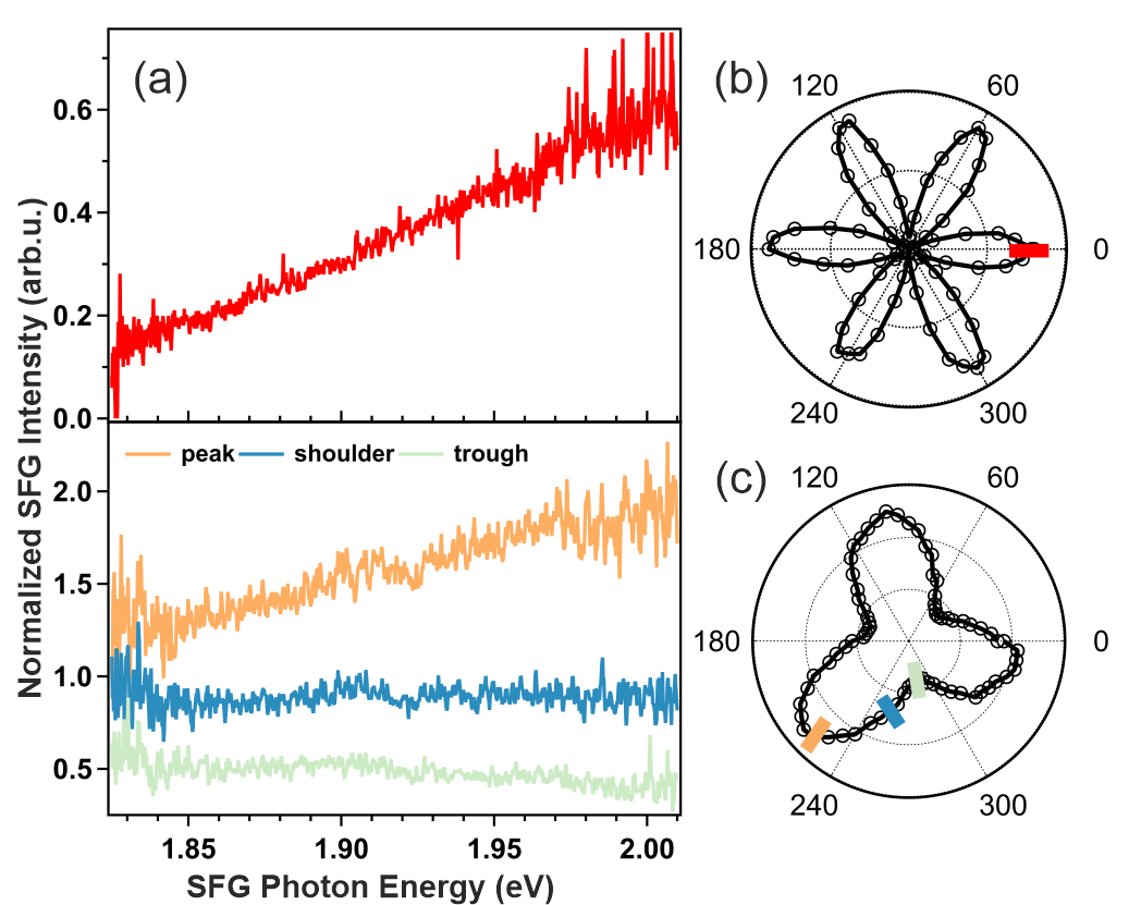
Figure 3(a) top and bottom panels show representative FS-SFG spectra of the \ceMoS2/Au sample under spp and ssp polarization combinations. Figure 3(b) and (c) are the corresponding azimuthal dependencies of the SFG intensity for the two polarization combinations. The azimuthal pattern for spp exhibits a six-fold symmetry, while that for ssp shows a three-fold symmetry. The reason for the different azimuthal symmetric pattern has been extensively discussed in our previous work [31]. In brief, for spp polarization, the SFG signal purely originates from the \ceMoS2, while on the other hand both \ceMoS2 and Au contribute to the SFG signal when using ssp polarization. In the latter case, the interference of the two signals results in a reduction in the symmetry from six-fold to three-fold.
In this work, we will focus on the spectra of these FS-SFG responses. For spp polarization combination, the spectral shape in the reported A and B exciton energy region is close to a straight line and the slope is independent of the azimuthal angle, only the intensities change (Here only a representative spectrum collected at the maximum integrated FS-SFG intensities, which is marked in red in Fig. 3(b) is presented). On the contrary, the spectral shape recorded under the ssp polarization combination (bottom panel of Fig. 3(a)) maintains a linear appearance, yet with slopes that exhibit significant sensitivity to the azimuthal angle (the weak narrow features around 1.92 eV are from the vibrational responses of the unavoidable hydrocarbon impurities being upconverted by the 1.56 eV visible beam). Specifically, at the azimuthal intensity maximum (highlighted in orange in Fig. 3(c)), the slope is positive; at the azimuthal intensity minimum (marked in light-green in Fig. 3(c)), the slope is negative. Furthermore, at the shoulder, the spectrum appears nearly horizontal (indicated by the blue marker in Fig. 3(c)), akin to the FS-SFG response observed in pure PVD Au (refer to Fig. S2 in the Supplemental Material [32]). To establish a reference, azimuthal-dependent SFG intensity and spectrum of \ceMoS2/\ceSiO2 were also obtained. A distinctive resonant peak is observed at 1.84 eV, attributed to the A exciton, as illustrated in Fig. S3 of the Supplemental Material [32]. Clearly, in the case of \ceMoS2/Au, even though the FS-SFG photon energy falls within the A and B exciton energy range, all the spectra display a linear profile, and no excitonic features were observed.
While both the PL (Fig. 2) and the FS-SFG (Fig. 3) spectra suggest a quench of the excitonic features, the implications of the two observations differ significantly. The quenched spectrum in PL solely implies a non-radiative relaxation process, and it does not provide any additional information such as bandgap renormalization or potential substrate induced doping. On the contrary, the FS-SFG spectra of \ceMoS2 on Au distinctly exhibit the radiative signal. A comprehensive analysis of this signal can provide valuable insights into the electronic properties of this intricate system.
One of the intriguing properties of 2D materials is their extreme sensitivity to the screening from the environment. Both theory [43, 44, 45] and experiments [46, 16] have shown that the screening from the environment or from the substrate doped free charge carriers inside the TMDC can effectively reduce the Coulomb interaction between electron-hole pairs, leading to an increase in their spatial separation and a reduction in the exciton’s binding energy. Depending on the nature of screening (dynamic or static), the quasiparticle bandgap may be reduced (known as bandgap renormalization) by the same amount as the change of the binding energy of the exciton [44]. Obviously, metals possess an extremely large dielectric constant and produce a strong doping effect compared to free-standing or dielectric substrate-supported conditions. Consequently, stable excitons cannot be formed in a \ceMoS2 monolayer on Au at room temperature, as evidenced by our observation.
As the formation of excitons within \ceMoS2/Au is not feasible, the isolated optical response of the \ceMoS2 hence can report the electronic property of the semiconductor at the band edge, similar to the Tauc plot method reported for bulk amorphous semiconductors [19]. Fig. 4 shows the results of such an analogous Tauc plot. A straight line is clearly obtained. Extrapolating the line in the plot to , as shown in Fig. 4, gives a value of eV as averaged from several independent measurements. Given that this response is approximately equivalent to the convolution of two constant DOS functions at the band edges (as confirmed by a DFT calculation), this value reports the onset of the bandgap at the K-point in the first Brillouin zone (see Supplemental Material [32] about the band structure and constant DOS).
The Tauc plot method has previously been utilized to determine the bandgap of TMDC thin films, without accounting for the impact of excitons [21, 22]. However, for a free-standing TMDC monolayer or a monolayer on a dielectric substrate, the presence of excitons due to insufficient screening, can significantly hinder the unambiguous identification of the absorption edge. In contrast, in the current study, the exciton binding energy is sufficiently low when the TMDC monolayer is placed on Au, so that the analogous Tauc plot becomes possible as long as the pure monolayer response can be extracted. It should be noted that in this study we directly plot the Fresnel factor corrected as a function of the sum frequency photon energy, rather than plotting as a function of the input photon energy . This approach is justified by the Miller theory in nonlinear optics [30], where the lineshapes of a final state resonance in a second-order nonlinear optical process are identical to those of a linear optical process such as optical absorption (see Supplemental Material [32] for further discussion).
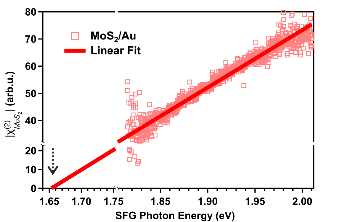
The quasiparticle bandgap obtained in this study is much smaller than that for free-standing or dielectric material supported \ceMoS2 monolayer. The screening effect from the substrate and from the additional charge carriers inside the monolayer via substrate doping may be the main reason. A tr-ARPES study revealed a direct electronic bandgap of 1.95 eV at the K-point [16]. However, it should be noted that the bandgap measured in their study refers to the energy difference between the center of the lowest conduction band and that of the highest valence bands at the K-point. Whereas the value extracted from our experiment is the onset of the difference between these two. Considering the full width at the half maximum (0.3 eV) of the bands in the tr-APRES results (Fig. 2 in ref [16]), our results are in agreement with theirs. In a STS study, a bandgap of eV was extracted from the STS spectra [13], aligning closely with our result. Additionally, different quasiparticle bandgap values, ranging from 1.6 to 2.9 eV, have been reported from previous calculations using different level of theories [47, 48, 44]. Our calculation provides new and reliable parameters for future comparison between the theory and experiment.
In addition to the electronic bandgap, the interfaces created when 2D semiconductors come into contact with 3D metallic electrodes play a pivotal role in many newly developed optoelectronic and photocatalytic devices [49, 50]. Our study offers a straightforward optical method to characterize the optical response of the 2D semiconductor itself with a non-contact manner. Such a method can be extended to other similar systems for devices based on the optoelectronic properties of TMDCs.
While our current research is both novel and informative, it is important to acknowledge certain limitations. Specifically, the limited probing frequency range is a result of constraints imposed by our experimental setup. Additionally, in the determination of the bandgap onset using the analogous Tauc plot, we had to employ an approximation based on Miller’s rule [30]. However, despite these constraints, our conclusions regarding the absence of A and B excitons and the observed reduction of the bandgap for \ceMoS2/Au are firmly rooted in the experimental data. To address these limitations and deepen our understanding, we plan to widen the optical window and conduct heterodyne SFG measurements in our future studies.
III Conclusion
Through careful polarization selection in the FS-SFG measurements, we were able to effectively isolate the \ceMoS2 monolayer’s optical response from the \ceMoS2/Au system. The significant screening effect induced by the Au substrate and by the doped free carriers inside the monolayer results in a substantial reduction of the exciton’s binding energy and remarkable bandgap renormalization, effectively impeding the formation of A and B excitons. Under these conditions, we could extract the expected linear onset of optical absorption of a TMDC semiconductor under a quasi-particle picture. Our study provides valuable insights for understanding the electronic properties at the 2D semiconductor and 3D metal junction with the help of DFT calculations. By introducing an analogous Tauc plot using the pure second-order nonlinear susceptibility (), we accurately determine a quasiparticle bandgap of eV. This methodology can be applied to various 2D semiconductor and 3D metal junctions, improving our understanding of optical properties in the presence of abundant free carriers and providing a valuable reference for the further development of photocatalysts.
Acknowledgements.
This work was funded by the Deutsche Forschungsgemeinschaft (DFG, German Research Foundation) through projects A06, B02, and C05 within the SFB 1242 "Non-Equilibrium Dynamics of Condensed Matter in the Time Domain" (project number 278162697), through Germany’s Excellence Strategy (EXC 2033 - 390677874 - RESOLV). Additional support was provided by the European Research Council, i.e., ERC- CoG-2017 SOLWET (project number 772286) to RKC.References
- Mak et al. [2010] K. F. Mak, C. Lee, J. Hone, J. Shan, and T. F. Heinz, Phys. Rev. Lett. 105, 136805 (2010).
- Splendiani et al. [2010] A. Splendiani, L. Sun, Y. Zhang, T. Li, J. Kim, C.-Y. Chim, G. Galli, and F. Wang, Nano Lett. 10, 1271 (2010).
- Wang et al. [2012] Q. H. Wang, K. Kalantar-Zadeh, A. Kis, J. N. Coleman, and M. S. Strano, Nat. Nanotechnol. 7, 699 (2012).
- Mak and Shan [2016] K. F. Mak and J. Shan, Nat. Photon. 10, 216 (2016).
- Mueller and Malic [2018] T. Mueller and E. Malic, npj 2D Mater Appl 2, 1 (2018).
- Liu et al. [2021] Y. Liu, X. Duan, H.-J. Shin, S. Park, Y. Huang, and X. Duan, Nature 591, 43 (2021).
- Radisavljevic et al. [2011] B. Radisavljevic, A. Radenovic, J. Brivio, V. Giacometti, and A. Kis, Nat. Nanotechnol. 6, 147 (2011).
- Yin et al. [2012] Z. Yin, H. Li, H. Li, L. Jiang, Y. Shi, Y. Sun, G. Lu, Q. Zhang, X. Chen, and H. Zhang, ACS Nano 6, 74 (2012).
- Bartolomeo et al. [2017] A. D. Bartolomeo, L. Genovese, F. Giubileo, L. Iemmo, G. Luongo, T. Foller, and M. Schleberger, 2D Mater. 5, 015014 (2017).
- Shi et al. [2016] J. Shi, R. Tong, X. Zhou, Y. Gong, Z. Zhang, Q. Ji, Y. Zhang, Q. Fang, L. Gu, X. Wang, Z. Liu, and Y. Zhang, Adv. Mater. 28, 10664 (2016).
- Guo et al. [2020] X. Guo, Q. Li, Y. Liu, T. Jin, Y. Chen, L. Guo, and T. Lian, ACS Appl. Mater. Interfaces 12, 44769 (2020).
- Strange et al. [2020] L. E. Strange, J. Yadav, S. Garg, P. S. Shinde, J. W. Hill, C. M. Hill, P. Kung, and S. Pan, J. Phys. Chem. Lett. 11, 3488 (2020).
- Bruix et al. [2016] A. Bruix, J. A. Miwa, N. Hauptmann, D. Wegner, S. Ulstrup, S. S. Grønborg, C. E. Sanders, M. Dendzik, A. Grubišić Čabo, M. Bianchi, J. V. Lauritsen, A. A. Khajetoorians, B. Hammer, and P. Hofmann, Phys. Rev. B 93, 165422 (2016).
- Silva et al. [2022] C. C. Silva, D. Dombrowski, N. Atodiresei, W. Jolie, F. F. z. Hagen, J. Cai, P. T. P. Ryan, P. K. Thakur, V. Caciuc, S. Blügel, D. A. Duncan, T. Michely, T.-L. Lee, and C. Busse, 2D Mater. 9, 025003 (2022).
- Wang et al. [2018] G. Wang, A. Chernikov, M. M. Glazov, T. F. Heinz, X. Marie, T. Amand, and B. Urbaszek, Rev. Mod. Phys. 90, 021001 (2018).
- Čabo et al. [2015] A. G. Čabo, J. A. Miwa, S. S. Grønborg, J. M. Riley, J. C. Johannsen, C. Cacho, O. Alexander, R. T. Chapman, E. Springate, M. Grioni, J. V. Lauritsen, P. D. C. King, P. Hofmann, and S. Ulstrup, Nano Lett. 15, 5883 (2015).
- Liu et al. [2019] F. Liu, M. E. Ziffer, K. R. Hansen, J. Wang, and X. Zhu, Phys. Rev. Lett. 122, 246803 (2019).
- Tauc [1968] J. Tauc, Materials Research Bulletin 3, 37 (1968).
- Klein et al. [2023] J. Klein, L. Kampermann, B. Mockenhaupt, M. Behrens, J. Strunk, and G. Bacher, Adv. Funct. Mater. n/a, 2304523 (2023).
- Grundmann [2016] M. Grundmann, The Physics of Semiconductors: An Introduction Including Nanophysics and Applications (Springer International Publishing, 2016).
- Zheng et al. [2020] W. Zheng, M. Bonn, and H. I. Wang, Nano Lett. 20, 5807 (2020).
- Paul and Grinberg [2022] A. Paul and I. Grinberg, Phys. Rev. Appl. 17, 024042 (2022).
- Mattinen et al. [2017] M. Mattinen, T. Hatanpää, T. Sarnet, K. Mizohata, K. Meinander, P. J. King, L. Khriachtchev, J. Räisänen, M. Ritala, and M. Leskelä, Adv. Mater. Interfaces 4, 1700123 (2017).
- Wang et al. [2021] S. Wang, J.-K. Huang, M. Li, A. Azam, X. Zu, L. Qiao, J. Yang, and S. Li, ACS Appl. Mater. Interfaces 13, 47962 (2021).
- Bhanu et al. [2015] U. Bhanu, M. R. Islam, L. Tetard, and S. I. Khondaker, Sci. Rep. 4, 5575 (2015).
- Pollmann et al. [2021] E. Pollmann, S. Sleziona, T. Foller, U. Hagemann, C. Gorynski, O. Petri, L. Madauß, L. Breuer, and M. Schleberger, ACS Omega 6, 15929 (2021).
- Zou et al. [2021] B. Zou, Z. Wu, Y. Zhou, Y. Zhou, J. Wang, L. Zhang, F. Cao, and H. Sun, Phys. Status Solidi RRL 15, 2100385 (2021).
- Park et al. [2018] S. Park, N. Mutz, T. Schultz, S. Blumstengel, A. Han, A. Aljarb, L.-J. Li, E. J. W. List-Kratochvil, P. Amsalem, and N. Koch, 2D Mater. 5, 025003 (2018).
- Shen [1989] Y. R. Shen, Nature 337, 519 (1989).
- Boyd [2020] R. W. Boyd, Nonlinear Optics (Academic Press, 2020).
- Yang et al. [2023] T. Yang, E. Pollmann, S. Sleziona, E. Hasselbrink, P. Kratzer, M. Schleberger, R. K. Campen, and Y. Tong, Phys. Rev. B 107, 155433 (2023).
- [32] .
- Tong et al. [2017] Y. Tong, F. Lapointe, M. Thämer, M. Wolf, and R. K. Campen, Angew. Chem., Int. Ed. 56, 4211 (2017).
- Tong et al. [2018] Y. Tong, I. Y. Zhang, and R. K. Campen, Nat. Commun. 9, 1313 (2018).
- Lee et al. [2010] C. Lee, H. Yan, L. E. Brus, T. F. Heinz, J. Hone, and S. Ryu, ACS Nano 4, 2695 (2010).
- Velický et al. [2020] M. Velický, A. Rodriguez, M. Bouša, A. V. Krayev, M. Vondráček, J. Honolka, M. Ahmadi, G. E. Donnelly, F. Huang, H. D. Abruña, K. S. Novoselov, and O. Frank, J. Phys. Chem. Lett. 11, 6112 (2020).
- Sarkar and Kratzer [2021] S. Sarkar and P. Kratzer, J. Phys. Chem. C 125, 26645 (2021).
- Xiao et al. [2012] D. Xiao, G.-B. Liu, W. Feng, X. Xu, and W. Yao, Phys. Rev. Lett. 108, 196802 (2012).
- Scheuschner et al. [2014] N. Scheuschner, O. Ochedowski, A.-M. Kaulitz, R. Gillen, M. Schleberger, and J. Maultzsch, Phys. Rev. B 89, 125406 (2014).
- Kumar et al. [2013] N. Kumar, S. Najmaei, Q. Cui, F. Ceballos, P. M. Ajayan, J. Lou, and H. Zhao, Phys. Rev. B 87, 161403 (2013).
- Malard et al. [2013] L. M. Malard, T. V. Alencar, A. P. M. Barboza, K. F. Mak, and A. M. de Paula, Phys. Rev. B 87, 201401 (2013).
- Jiang et al. [2014] T. Jiang, H. Liu, D. Huang, S. Zhang, Y. Li, X. Gong, Y.-R. Shen, W.-T. Liu, and S. Wu, Nat. Nanotechnol. 9, 825 (2014).
- Olsen et al. [2016] T. Olsen, S. Latini, F. Rasmussen, and K. S. Thygesen, Phys. Rev. Lett. 116, 056401 (2016).
- Drüppel et al. [2017] M. Drüppel, T. Deilmann, P. Krüger, and M. Rohlfing, Nat. Commun. 8, 2117 (2017).
- Steinhoff et al. [2018] A. Steinhoff, T. O. Wehling, and M. Rösner, Phys. Rev. B 98, 045304 (2018).
- Ugeda et al. [2014] M. M. Ugeda, A. J. Bradley, S.-F. Shi, F. H. da Jornada, Y. Zhang, D. Y. Qiu, W. Ruan, S.-K. Mo, Z. Hussain, Z.-X. Shen, F. Wang, S. G. Louie, and M. F. Crommie, Nat. Mater. 13, 1091 (2014).
- Cheiwchanchamnangij and Lambrecht [2012] T. Cheiwchanchamnangij and W. R. L. Lambrecht, Phys. Rev. B 85, 205302 (2012).
- Kormányos et al. [2015] A. Kormányos, G. Burkard, M. Gmitra, J. Fabian, V. Zólyomi, N. D. Drummond, and V. Fal’ko, 2D Mater. 2, 022001 (2015).
- Wang et al. [2019] Y. Wang, J. C. Kim, R. J. Wu, J. Martinez, X. Song, J. Yang, F. Zhao, A. Mkhoyan, H. Y. Jeong, and M. Chhowalla, Nature 568, 70 (2019).
- Shen et al. [2021] P.-C. Shen, C. Su, Y. Lin, A.-S. Chou, C.-C. Cheng, J.-H. Park, M.-H. Chiu, A.-Y. Lu, H.-L. Tang, M. M. Tavakoli, G. Pitner, X. Ji, Z. Cai, N. Mao, J. Wang, V. Tung, J. Li, J. Bokor, A. Zettl, C.-I. Wu, T. Palacios, L.-J. Li, and J. Kong, Nature 593, 211 (2021).