Coupling conduction-band valleys in modulated SiGe heterostructures via shear strain
Abstract
Engineering conduction-band valley couplings is a key challenge for Si-based spin qubits. Recent work has shown that the most reliable method for enhancing valley couplings entails adding Ge concentration oscillations to the quantum well. However, ultrashort oscillation periods are difficult to grow, while long oscillation periods do not provide useful improvements. Here, we show that the main benefits of short-wavelength oscillations can be achieved in long-wavelength structures through a second-order coupling process involving Brillouin-zone folding induced by shear strain. Moreover, we find that the same long-wavelength period also boosts spin-orbit coupling. We finally show that such strain can be achieved through common fabrication techniques, making this an exceptionally promising system for scalable quantum computing.
Si/SiGe quantum dots are an attractive platform for quantum computation [1, 2, 3], as demonstrated by recent experiments [4, 5, 6] where both single and two-qubit gate fidelities have exceeded the error correction threshold of [7]. However, Si/SiGe quantum dots suffer from small energy spacings between the ground and excited valley states [8], called valley splittings, , which induce leakage if they are small [9]. Popular strategies for enhancing include engineering atomically sharp interfaces [10, 11, 12] or narrow quantum wells [13, 14]. Unfortunately, random-alloy disorder [13] causes to vary significantly from dot to dot [14, 15], with typical values ranging from to [16, 17, 18, 19, 20, 21, 22, 23, 24].
The Wiggle Well (WW) has recently emerged as an important tool for enhancing the valley splitting, by adding Ge concentration oscillations (“wiggles") of wavelength to the Si quantum well [25]. Theoretical estimates suggest that these wiggles could provide a remarkable boost of for an average Ge concentration of only [26]. However, the small wavelength needed for this structure () corresponds to roughly two atomic monolayers, suggesting that such growth would be very challenging. Naive band-structure estimates also identify a second, longer , that could produce a large by coupling valleys in neighboring Brillouin zones. However, rigorous calculations [26] show that this coupling is inhibited by the nonsymmorphic screw symmetry of the Si crystal [27].
In this work, we show that a modified structure called a strain-assisted Wiggle Well (STRAWW) can overcome these problems. This device combines a long-wavelength WW (), which has already been demonstrated in the laboratory [25], with an experimentally feasible level of shear strain. We further show that valley splitting in STRAWW is largely independent of both the vertical electric field and the interface sharpness, thus simplifying heterostructure growth. Finally, we note that STRAWW should also boost the spin-orbit coupling, compared to conventional Si/SiGe quantum wells [27], thus enabling fast spin manipulation via electric dipole spin resonance, without a micromagnet. The combination of large valley splitting and large spin-orbit coupling makes STRAWW a very attractive platform for Si spin qubits. Below, we first provide an overview of the physics and implementation of strain in the STRAWW proposal, and then present calculations showing deterministically enhanced valley splittings.
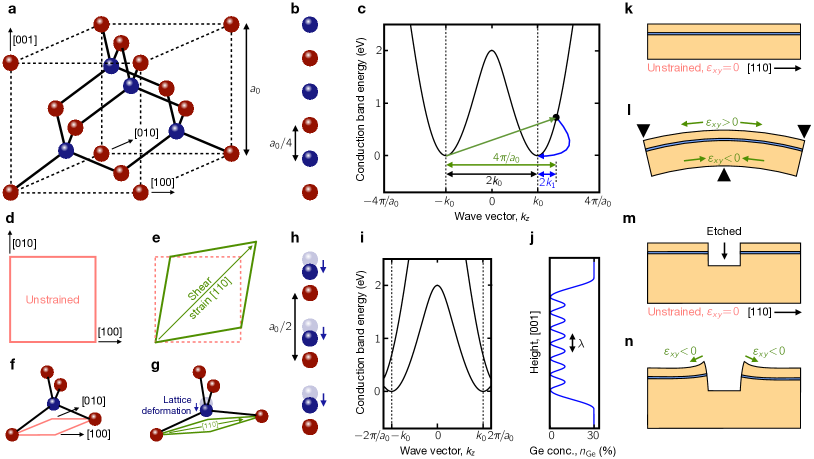
Shear strain has a subtle but profound effect on the silicon crystal lattice shown in Fig. 1a. In Fig. 1b, we also show an effective 1D lattice obtained by assuming translational symmetry along and and performing a Fourier transformation. (This 1D model forms the starting point for the effective-mass theory described below.) The conventional primitive unit cell of Si contains two atoms (red and blue), which give rise to the two sublattices shown in the figure. Now, for the special case of , silicon possesses a screw symmetry, which interchanges the red and blue lattices, and reduces the primitive cell to one atom [27]. The Brillouin zone along can then be expanded from to , as shown in Fig. 1c. Here is the size of the cubic unit cell, and the low-energy valley minima are located at . A short-period WW – if it could be grown – would provide a direct (i.e., first-order) coupling between the valleys, by introducing ultrashort-period Ge concentration oscillations into the quantum well (Fig. 1j), with [25, 26]. Here, we propose a more physically realistic, second-order coupling scheme involving (i) shear strain, which couples states separated by (green arrow in Fig. 1c), and (ii) a long-period WW of wavelength (blue arrow in Fig. 1c).
The mechanism responsible for the strain-induced coupling is illustrated in Figs. 1d-1g. Here, shear strain is seen to elongate and compress the crystal along the and directions, respectively. In turn, this distorts the tetrahedral bonds of the diamond lattice and shifts the blue sublattice downward with respect to the red sublattice (along ), as shown in Figs. 1g and 1h. This layer pairing causes the primitive cell to expand from one to two atoms, and the BZ folds back to the conventional boundaries at (Fig. 1i). The period of the distortion is , which gives the desired coupling vector upon Fourier transformation, and produces an avoided crossing of the low-energy bands, as observed at the zone boundary.
The second-order process illustrated in Fig. 1c couples the two valleys through a virtual (i.e., high-energy) state, indicated by a black dot. The resulting momentum loop can be expressed as , where the Ge concentration period corresponds precisely to the long-wavelength WW. We note that this period is 5.3 times larger than the period for the short-wavelength WW [26], making it experimentally feasible [25]. We also note that such large strains are commonly employed in the microelectronics industry [28, 29], where they are used to improve transistor performance. In the laboratory, we envision implementing shear strain through simple mechanical deformations, like those illustrated in Figs. 1k and 1l, for near-term experiments. In the long term, scalable solutions will likely involve etched geometries, like those illustrated in Figs. 1m and 1n, or other stressor-based strategies used in industry. Below, we simulate several shear-strain geometries that could be implemented in experiments, obtaining strain levels sufficient for achieving deterministically enhanced valley splittings greater than 100 eV. These results indicate that the STRAWW proposal is feasible and can be achieved with existing technology.
We now perform numerical simulations to quantify the effects of shear strain and Ge oscillations on the valley splitting, finding that significant enhancements are observed only when both features are present. We begin by employing an sp3d5s∗ tight-binding model [30, 31], which is known to give accurate results for the band structure over a wide range of energies (see Methods). The model incorporates tight-binding parameters for Si-Si, Ge-Ge, and Si-Ge nearest-neighbor hoppings, and can therefore describe arbitrary alloys. The model also includes strain, yielding results that are in good agreement with experimentally measured deformation potentials [30]. Here, we focus on the deterministic component of , ignoring local fluctuations of the Ge concentration [13]. The SiGe alloy is therefore treated in a virtual crystal approximation, following Ref. [27], where the Hamiltonian matrix elements are averaged over all possible alloy realizations.
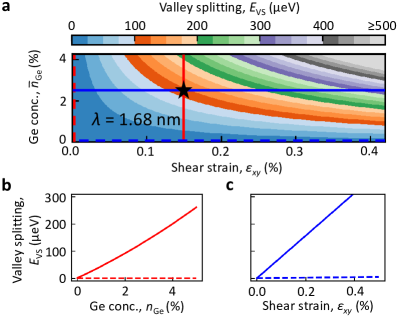
In Fig. 2, we plot the valley splitting as a function of the shear strain and the average Ge concentration in the quantum well . We consider a uniform vertical electric field of strength mV/nm and the optimal STRAWW oscillation wavelength of . We also assume a wide interface of width , as defined in Methods, which strongly suppresses the interface-induced valley splitting [13] and ensures that the valley splitting enhancements we observe here are caused by the STRAWW structure. Figure 2a shows results in the two-dimensional parameter space, while Fig. 2b shows two vertical linecuts, and Fig. 2c shows two horizontal linecuts, including the cases with or . These results clearly indicate that a combination of shear strain and concentration oscillations is needed to produce a large valley splitting. Indeed, when or , we observe dangerously low values of , over the whole parameter range. In contrast, when both , we quickly approach a range of acceptable valley splittings. For example, when and (black star in Fig. 2a), we obtain .

In Fig. 3, we show that the valley splitting enhancements observed in Fig. 2 are robust to imperfect implementation of the STRAWW wavelength nm. Plotting as a function of and in Fig. 3a, or in Fig. 3b, we find that a broad range of values gives acceptable valley splittings. For example, at the physically realistic device setting indicated by a black star (the same setting as Fig. 2), we obtain eV; on either side of this point, the range of wavelengths with eV extends from -1.9 nm, which is well within the growth tolerance achieved in Ref. [25]. Finally, we note that, near the optimal wavelength nm, varies linearly with both and , which we now explain using effective-mass theory.
To gain further insight into the separate (or combined) contributions to the valley splitting from shear strain and Ge concentration oscillations, we outline here an effective-mass theory, with details given in Supplementary Sec. 1. Treating the valleys centered at as pseudospins, the Hamiltonian takes the form
| (1) |
where is the intra-valley Hamiltonian and describes the inter-valley couplings. The intra-valley Hamiltonian is given by
| (2) |
where is the longitudinal effective mass, and
| (3) |
where the first term describes potential modulations of amplitude due to the Ge oscillations, and describes both the quantum-well confinement potential and the applied electric field. The inter-valley Hamiltonian takes the form
| (4) |
where and are constants, and is adjusted to match the valley splitting results from our sp3d5s∗ calculations. It is interesting to see two types of “fast” oscillations in this equation (indicated in Fig. 1c), with wavevectors arising from the potential, and arising from the shear strain.
We solve for the low-energy states of Eq. (1) using an envelope function method similar to [32] (see also Methods) by treating and perturbatively. Defining as the ground state of in Eq. (2), this analysis yields a simple but extremely useful expression for the inter-valley matrix element, :
| (5) |
where is the envelope function of (obtained by setting ), and we have defined the oscillation wavevector and oscillation energy scales as and , respectively. Note here that .
Each of the four terms in Eq. (5) effectively averages to zero for smoothly varying and , except when specific resonance conditions are met, and each term has a distinct physical origin and meaning, as explained below. The first term is the usual inter-valley matrix element in the absence of Ge oscillations and shear strain [13]. The second term describes Ge oscillations, independent of shear strain, and is the basis for the short-wavelength WW [25, 26]. The third term describes the shear strain contribution, independent of Ge oscillations. The fourth term involves both shear strain and Ge oscillations, and is unique to STRAWW. The resonance condition for which this term has a vanishing exponential, , corresponds to the long-period WW, or .
We can evaluate Eq. (5) for a specific quantum well model. For simplicity, we treat the quantum well as a harmonic confining potential with , and the envelope function , where is the characteristic dot size in the growth direction. Equation (5) then reduces to
| (6) |
If we now assume a long-period WW, with , the first three terms in Eq. (6) are all exponentially suppressed, leaving . This confirms the anticipated linear dependence on and , and provides a simple estimate for the STRAWW valley splitting. We also note that this expression is independent of , justifying our approximate treatment of the quantum well confining potential, and indicating that the valley splitting does not depend on the interface for this smooth quantum-well geometry.
In the opposite limit of an ultra-sharp interface, Eq. (6) is no longer accurate. In this case, the singular nature of the confining potential (or the envelope function ) generates Fourier components that cancel out the fast-oscillating phase factors in Eq. (5), so the first three terms are not suppressed. The resulting valley splitting enhancement has been studied previously for quantum wells with [33, 34, 35] and without [13] shear strain. However in the latter case, the crossover between ultra-sharp vs smooth interfaces occurs for interface widths of just 1-2 atomic monolayers, which are extremely difficult to grow in the laboratory [15], so valley splitting enhancements are rarely observed. In Supplementary Sec. II, we show numerically that the same is true for shear-strained structures, suggesting that the STRAWW strategy is much more practical.
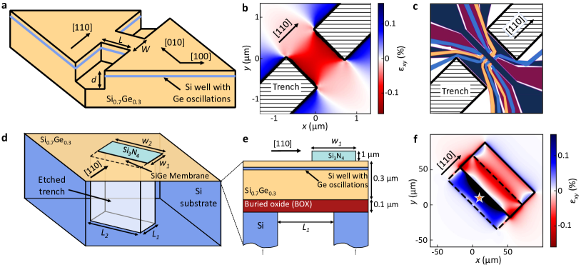
Finally, we show that the shear strains needed to deterministically enhance the valley splitting can be achieved with current micro and nanofabrication technologies. In Fig. 4, we consider two etching strategies. Figure 4a shows a microbridge geometry [36, 37], formed by etching the top surface to well below the quantum well. Here, the trenches are aligned along the crystallographic direction to provide shear strain in the channel region between the trenches. We calculate the strain in the quantum well numerically, using COMSOL Multiphysics [38], for the geometry shown in Fig. 4a, with . The resulting shear strain shown in Fig. 4b is largely uniform across the channel, except for edge strips with an approximate width of 100 nm. At the center of the channel, we obtain , which yields a large , even for a moderate WW amplitude (see Fig. 2). In this geometry, the trenches are well separated to avoid interfering with electrode fabrication, for example, using the gate design shown in Fig. 4c, which is similar to Ref. [24]. To allow for a higher density of gate electrodes, we envision filling the trenches with an oxide material, to restore a planar top surface on which additional gates can be fabricated.
Figures 4d and 4e show a second, stressor-type geometry, featuring a Si/SiGe heterostructure grown atop a buried oxide (BOX) layer [39], which serves as an etch-stop for a trench etched from the bottom of the Si substrate. The latter is aligned along [110], creating a free-standing Si/SiGe membrane [40, 41], which is readily strained by a stressor [42, 43, 44] (also aligned along [110]), due to the thinness of the membrane. For the geometry defined by , we obtain the strain results shown in Fig. 4f, where we assume a depositional tensile stress of for the stressor [42]. Here, the red region is covered by stressor, while the blue region is uncovered, but located above the trench. This blue region, which is most convenient for fabricating gates, provides a high and largely uniform shear strain, with at the location of the orange star, and over a wide area () that could potentially contain many dots in a dense two-dimensional array [45, 46, 47, 48].
In summary, we have shown that the combination of shear strain and the long-period Wiggle Well, dubbed “STRAWW,” is particularly effective for deterministically enhancing the valley splitting, which is a key missing ingredient for scaling up silicon spin qubits to large arrays. Effective-mass theory shows that this enhancement arises from a second-order coupling process that requires breaking the screw symmetry of the diamond lattice. Numerically accurate tight-binding simulations suggest that valley splittings needed for qubit operation can be achieved using realistic shear strains (%), while the required Ge concentration oscillations ( nm) have already been demonstrated in the laboratory [25]. Strain simulations confirm that several different etching techniques could be used to achieve such strain. Overall, the fabrication requirements for STRAWW are much less challenging than other schemes, including ultra-sharp interfaces and short-period Wiggle Wells, making this a very attractive approach for managing valley splitting in future qubit experiments. Moreover, spin-orbit coupling is also enhanced in long-period Wiggle Wells, which may be exploited for qubit manipulation [27]. We expect that future devices could provide shear strains larger than those reported here, through a variety of implementation strategies.
Methods
sp3d5s* tight-binding model
We use an sp3d5s∗ tight-binding model [30] to study valley coupling in Si/SiGe quantum wells. This is an atomistic model with nearest-neighbor hopping terms, including ten spatial orbitals at each atom site. Such models are well established for accurately modeling the electronic structure of many different semiconductors [31]. Spin-orbit coupling is typically introduced into these tight-binding models through an intra-atomic coupling between p orbitals [49]. However, this has no quantitative effect on the valley splitting results studied here, and is therefore disabled in the current analysis, for simplicity. On the other hand, we incorporate distinct Si-Si, Ge-Ge, and Si-Ge nearest-neighbor hopping terms, following [30], to more accurately represent SiGe alloys.
Strain is incorporated into the model through the equation
| (7) |
which relates the location of atom in the presence of strain () to its unperturbed location (). Here, is the strain tensor, the signs and are assigned depending on whether atom belongs to the red or blue sublattice, respectively (see Fig. 1a), and is Kleinman’s internal strain parameter [50], which is used in diamond crystal lattices to account for the relative shift of the two sublattices within a unit cell due to shear strain. We ignore the small difference between values for Si vs Ge atoms, simply adopting throughout the structure [51]. Strain is then incorporated into the tight-binding Hamiltonian in two ways: (i) strain-dependent onsite couplings, following [30], and (ii) modified bond lengths and angles, which result in modified hopping terms [52, 53]. Further details on our implementation of the sp3d5s∗ tight-binding model are provided in [27].
We consider a sigmoidal model for the Ge concentration profile in the tight-binding calculations, given by
| (8) |
where is the Ge concentration in the barrier region, is the interface width, is the average Ge concentration in the quantum well (associated with the Ge concentration oscillations), and is the oscillation wavelength. Note that the Ge concentration oscillations in Eq. (8) extend across the heterostructure (including the barrier region). In realistic devices, the Ge oscillations would likely only occur in the quantum well region, as illustrated in Fig. 1j. However, restricting the oscillations to the well region in the simulations produces kinks in profile, which are known to artificially boost the valley by enlarging the short-wavelength Fourier components of [13]. Such kinks are not expected to be present in realistic devices. We therefore avoid any such effects here by extending the Ge concentration oscillations across the whole structure. We also note that the bottom quantum well interface has been excluded in Eq. (8), because the electric field used in our simulations is always large enough to push the electron wave function tightly against the top interface.
Envelope-function method
Here, we use an envelope-function approach to derive Eq. (5) of the main text within the effective-mass framework of Eq. (1). To begin, we note that the energy scale of the intra-valley Hamiltonian dominates over the inter-valley Hamiltonian . We can therefore calculate by first solving for the ground state of , and then computing the matrix element of within first-order perturbation theory.
We can solve straightforwardly with an effective-mass approximation. First, we note that the ground state of (or any other eigenstate) may be expanded as [32]
| (9) |
where comprises a complete and orthogonal set of Bloch functions that satisfy the Bloch-Schrödinger equation,
| (10) |
and are envelope functions that account for the effects of the confinement, . Note that the Bloch functions here do not have the periodic structure of the crystal lattice, but rather the periodic structure of the WW, which enters through the potential in Eq. (3). are therefore periodic over the length scale , while are slowly varying over this length scale. Here we adopt the conventional normalizations and . Plugging Eq. (9) into the Schrödinger equation yields the coupled envelope equations
| (11) |
where
| (12) |
and , and is a non-local potential arising from , whose form is given in Ref. [32].
Up to this point, the expansion of Eq. (9) and the following equations are exact. However, the Schrödinger-like, coupled envelope equations, Eq. (11), can be effectively decoupled via a canonical transformation, yielding the much simpler result, , where satisfies an effective mass equation. To derive this result, we note that the non-local and inter-band nature of the potential arises from the Fourier components of in the outer-half of the Brillouin zone, i.e. for large wavevectors . Assuming that varies slowly compared to , these Fourier components are insignificant, and we can ignore all non-local and inter-band components in . In other words, there is a separation of length scales leading to the following local approximation [32] for Eq. (11):
| (13) |
Now, there is also a large separation of energy scales that we can use to simplify the envelope equations. The largest energy scale in Eq. (13), by far, is the splitting between the different Bloch modes, . In the absence of coupling between these Bloch modes (i.e., for ), the confinement energy scale arising from is of order of , where is the width of the quantum well, while the inter-mode coupling term, which scales as is intermediate between these two energy scales. A perturbative treatemenmt of the coupling is therefore justified. Applying a Schrieffer-Wolff transformation, we obtain the desired single-mode solution , where satisfies the effective-mass equation,
| (14) |
and the renormalized effective mass is given by
| (15) |
Equation (14) is a standard effective-mass equation, where the periodic potential associated with the WW has been absorbed into the renormalized effective mass. However, the effective-mass correction () is very small for typical heterostructures, since , while for , such that . It is therefore a very good approximation to ignore the effective-mass renormalization. The leading-order correction in this formalism () appears only in the Bloch function , which to leading-order in is given by
| (16) |
Finally, we are in a position to compute the inter-valley matrix element using . The result contains many terms, but is greatly simplified by ignoring the higher-order terms, terms involving derivatives of , and integrals containing highly oscillatory plane waves that average toward zero. [Note that terms involving derivatives of the envelope function are insignificant, because the are slowly varying compared to the fast-oscillating terms.] A straightforward calculation then leads to Eq. (5) in the main text, and the corresponding valley splitting is given by .
Strain calculations
Shear strain calculations were performed using the Solid Mechanics module in COMSOL Multiphysics [38]. Below, we describe the materials properties assumed in these simulations, including the coefficients of thermal expansion (CTE), which describe thermal contractions when the device is cooled from room temperature (293.15 K) to 1 K.
For the top-trench geometry of Fig. 4a, we assume a quantum well formed of a strained-silicon layer sandwiched between a thick strain-relaxed buffer layer and a 50 nm top layer of strain-relaxed . In a typical device, we would assume a buffer layer thickness of order 500 m, which is challenging to simulate. In our simulations, we approximately account for such thick layers by assuming a thinner layer of width 2 m (which is still much thicker than the top layers), and adopting a zero-displacement boundary condition, as defined in [38]. The total volume of the resulting simulation is about . Biaxial strain is applied to the Si layer through the initial-strain parameters , and .
The CTEs of Si and SiGe depend weakly on temperature, while COMSOL assumes constant CTE values. To account for this in our simulations, we simply adjust the CTE values in the COMSOL parameter library. Averaging over the CTEs provided in Refs. [55, 56, 57] and applying Vegard’s law to describe the SiGe alloy, we find the temperature-adjusted coefficients to be for Si, and for the SiGe. For both Young’s modulus and the Poisson ratio , thermal corrections amount to only a few percent at most; we therefore use room temperature values for these parameters, as given in the COMSOL parameter library. To fully account for the Si buffer layer (which is not included in the simulation), we also include the thermally corrected Si CTE, , to describe the contraction of the bottom surface of the simulated device. To check the validity of our approximate treatment of the thick buffer layer, we also simulate thicker systems, to check for convergence, and we relax the boundary conditions by applying COMSOL’s rigid-motion-suppression feature.
For the free-standing membrane geometry shown in Fig. 4d, we adopt the heterostructure parameters shown in Fig. 4e. We also assume a trench height of . Here, we simulate a much larger total volume of about , to more accurately describe the effects of the deep trench. Biaxial strain is imposed as described above, and we account for depositional strain in the stressor by imposing an intrinsic tensile stress of [42]. Here again we relax the boundary conditions using COMSOL’s rigid-motion-suppression feature. To account for thermal contraction, we take the same approach as above, with the additional temperature-adjusted CTEs given by and [58, 59, 60]. We note that nearly identical shear-strain results can be obtained using room-temperature CTE values from the COMSOL library without accounting for cryogenic cooling, indicating that depositional strain from the stressor dominates over thermal contraction in this geometry.
References
- Loss and DiVincenzo [1998] D. Loss and D. P. DiVincenzo, Quantum computation with quantum dots, Phys. Rev. A 57, 120 (1998).
- Hanson et al. [2007] R. Hanson, L. P. Kouwenhoven, J. R. Petta, S. Tarucha, and L. M. K. Vandersypen, Spins in few-electron quantum dots, Rev. Mod. Phys. 79, 1217 (2007).
- Burkard et al. [2023] G. Burkard, T. D. Ladd, A. Pan, J. M. Nichol, and J. R. Petta, Semiconductor spin qubits, Rev. Mod. Phys. 95, 025003 (2023).
- Xue et al. [2022] X. Xue, M. Russ, N. Samkharadze, B. Undseth, A. Sammak, G. Scappucci, and L. M. K. Vandersypen, Quantum logic with spin qubits crossing the surface code threshold, Nature 601, 343 (2022).
- Noiri et al. [2022] A. Noiri, K. Takeda, T. Nakajima, T. Kobayashi, A. Sammak, G. Scappucci, and S. Tarucha, Fast universal quantum gate above the fault-tolerance threshold in silicon, Nature 601, 338 (2022).
- Mills et al. [2022] A. R. Mills, C. R. Guinn, M. J. Gullans, A. J. Sigillito, M. M. Feldman, E. Nielsen, and J. R. Petta, Two-qubit silicon quantum processor with operation fidelity exceeding 99%, Science Advances 8, eabn5130 (2022).
- Fowler et al. [2012] A. G. Fowler, M. Mariantoni, J. M. Martinis, and A. N. Cleland, Surface codes: Towards practical large-scale quantum computation, Phys. Rev. A 86, 032324 (2012).
- Zwanenburg et al. [2013] F. A. Zwanenburg, A. S. Dzurak, A. Morello, M. Y. Simmons, L. C. L. Hollenberg, G. Klimeck, S. Rogge, S. N. Coppersmith, and M. A. Eriksson, Silicon quantum electronics, Rev. Mod. Phys. 85, 961 (2013).
- Buterakos and Das Sarma [2021] D. Buterakos and S. Das Sarma, Spin-valley qubit dynamics in exchange-coupled silicon quantum dots, PRX Quantum 2, 040358 (2021).
- Boykin et al. [2004a] T. B. Boykin, G. Klimeck, M. A. Eriksson, M. Friesen, S. N. Coppersmith, P. von Allmen, F. Oyafuso, and S. Lee, Valley splitting in strained silicon quantum wells, Applied Physics Letters 84, 115 (2004a).
- Boykin et al. [2004b] T. B. Boykin, G. Klimeck, M. Friesen, S. N. Coppersmith, P. von Allmen, F. Oyafuso, and S. Lee, Valley splitting in low-density quantum-confined heterostructures studied using tight-binding models, Phys. Rev. B 70, 165325 (2004b).
- Friesen et al. [2007] M. Friesen, S. Chutia, C. Tahan, and S. N. Coppersmith, Valley splitting theory of quantum wells, Phys. Rev. B 75, 115318 (2007).
- Losert et al. [2023] M. P. Losert, M. A. Eriksson, R. Joynt, R. Rahman, G. Scappucci, S. N. Coppersmith, and M. Friesen, Practical strategies for enhancing the valley splitting in Si/SiGe quantum wells, arXiv:2303.02499 (2023).
- Chen et al. [2021] E. H. Chen, K. Raach, A. Pan, A. A. Kiselev, E. Acuna, J. Z. Blumoff, T. Brecht, M. D. Choi, W. Ha, D. R. Hulbert, M. P. Jura, T. E. Keating, R. Noah, B. Sun, B. J. Thomas, M. G. Borselli, C. Jackson, M. T. Rakher, and R. S. Ross, Detuning axis pulsed spectroscopy of valley-orbital states in Si/Si-Ge Quantum Dots, Phys. Rev. Appl. 15, 044033 (2021).
- Wuetz et al. [2022] B. Paquelet Wuetz, M. P. Losert, S. Koelling, L. E. A. Stehouwer, A.-M. J. Zwerver, S. G. J. Philips, M. T. Mądzik, X. Xue, G. Zheng, M. Lodari, S. V. Amitonov, N. Samkharadze, A. Sammak, L. M. K. Vandersypen, R. Rahman, S. N. Coppersmith, O. Moutanabbir, M. Friesen, and G. Scappucci, Atomic fluctuations lifting the energy degeneracy in Si/SiGe quantum dots, Nature Commun. 13, 7730 (2022).
- Borselli et al. [2011] M. G. Borselli, R. S. Ross, A. A. Kiselev, E. T. Croke, K. S. Holabird, P. W. Deelman, L. D. Warren, I. Alvarado-Rodriguez, I. Milosavljevic, F. C. Ku, W. S. Wong, A. E. Schmitz, M. Sokolich, M. F. Gyure, and A. T. Hunter, Measurement of valley splitting in high-symmetry Si/SiGe quantum dots, Appl. Phys. Lett. 98, 123118 (2011).
- Zajac et al. [2015] D. M. Zajac, T. M. Hazard, X. Mi, K. Wang, and J. R. Petta, A reconfigurable gate architecture for Si/SiGe quantum dots, Appl. Phys. Lett. 106, 223507 (2015).
- Mi et al. [2017] X. Mi, C. G. Péterfalvi, G. Burkard, and J. R. Petta, High-resolution valley spectroscopy of Si quantum dots, Phys. Rev. Lett. 119, 176803 (2017).
- Scarlino et al. [2017] P. Scarlino, E. Kawakami, T. Jullien, D. R. Ward, D. E. Savage, M. G. Lagally, M. Friesen, S. N. Coppersmith, M. A. Eriksson, and L. M. K. Vandersypen, Dressed photon-orbital states in a quantum dot: Intervalley spin resonance, Phys. Rev. B 95, 165429 (2017).
- Neyens et al. [2018] S. F. Neyens, R. H. Foote, B. Thorgrimsson, T. J. Knapp, T. McJunkin, L. M. K. Vandersypen, P. Amin, N. K. Thomas, J. S. Clarke, D. E. Savage, M. G. Lagally, M. Friesen, S. N. Coppersmith, and M. A. Eriksson, The critical role of substrate disorder in valley splitting in Si quantum wells, Appl. Phys. Lett. 112, 243107 (2018).
- Mi et al. [2018] X. Mi, S. Kohler, and J. R. Petta, Landau-zener interferometry of valley-orbit states in Si/SiGe double quantum dots, Phys. Rev. B 98, 161404 (2018).
- Borjans et al. [2019] F. Borjans, D. Zajac, T. Hazard, and J. Petta, Single-Spin Relaxation in a Synthetic Spin-Orbit Field, Phys. Rev. Appl. 11, 044063 (2019).
- Hollmann et al. [2020] A. Hollmann, T. Struck, V. Langrock, A. Schmidbauer, F. Schauer, T. Leonhardt, K. Sawano, H. Riemann, N. V. Abrosimov, D. Bougeard, and L. R. Schreiber, Large, tunable valley splitting and single-spin relaxation mechanisms in a / quantum dot, Phys. Rev. Appl. 13, 034068 (2020).
- Dodson et al. [2022] J. P. Dodson, H. E. Ercan, J. Corrigan, M. P. Losert, N. Holman, T. McJunkin, L. F. Edge, M. Friesen, S. N. Coppersmith, and M. A. Eriksson, How valley-orbit states in silicon quantum dots probe quantum well interfaces, Phys. Rev. Lett. 128, 146802 (2022).
- McJunkin et al. [2022] T. McJunkin, B. Harpt, Y. Feng, M. P. Losert, R. Rahman, J. P. Dodson, M. A. Wolfe, D. E. Savage, M. G. Lagally, S. N. Coppersmith, M. Friesen, R. Joynt, and M. A. Eriksson, SiGe quantum wells with oscillating Ge concentrations for quantum dot qubits, Nature Commun. 13, 7777 (2022).
- Feng and Joynt [2022] Y. Feng and R. Joynt, Enhanced valley splitting in Si layers with oscillatory Ge concentration, Phys. Rev. B 106, 085304 (2022).
- Woods et al. [2023] B. D. Woods, M. A. Eriksson, R. Joynt, and M. Friesen, Spin-orbit enhancement in Si/SiGe heterostructures with oscillating Ge concentration, Phys. Rev. B 107, 035418 (2023).
- Auth [2008] C. Auth, 45nm high-k + metal gate strain-enhanced CMOS transistors, in 2008 IEEE Custom Integrated Circuits Conference (2008) pp. 379–386.
- Packan et al. [2008] P. Packan, S. Cea, H. Deshpande, T. Ghani, M. Giles, O. Golonzka, M. Hattendorf, R. Kotlyar, K. Kuhn, A. Murthy, P. Ranade, L. Shifren, C. Weber, and K. Zawadzki, High performance Hi-K + metal gate strain enhanced transistors on (110) silicon, in 2008 IEEE International Electron Devices Meeting (2008) pp. 1–4.
- Niquet et al. [2009] Y. M. Niquet, D. Rideau, C. Tavernier, H. Jaouen, and X. Blase, Onsite matrix elements of the tight-binding Hamiltonian of a strained crystal: Application to silicon, germanium, and their alloys, Phys. Rev. B 79, 245201 (2009).
- Jancu et al. [1998] J.-M. Jancu, R. Scholz, F. Beltram, and F. Bassani, Empirical tight-binding calculation for cubic semiconductors: General method and material parameters, Phys. Rev. B 57, 6493 (1998).
- Burt [1988] M. G. Burt, An exact formulation of the envelope function method for the determination of electronic states in semiconductor microstructures, Semiconductor Science and Technology 3, 739 (1988).
- Ungersboeck et al. [2007] E. Ungersboeck, S. Dhar, G. Karlowatz, V. Sverdlov, H. Kosina, and S. Selberherr, The Effect of General Strain on the Band Structure and Electron Mobility of Silicon, IEEE Transactions on Electron Devices 54, 2183 (2007).
- Sverdlov and Selberherr [2008] V. Sverdlov and S. Selberherr, Electron subband structure and controlled valley splitting in silicon thin-body SOI FETs: Two-band k·p theory and beyond, Solid-State Electronics 52, 1861 (2008).
- Adelsberger et al. [2023] C. Adelsberger, S. Bosco, J. Klinovaja, and D. Loss, Valley-free silicon fins by shear strain, arXiv:2308.134486 (2023).
- Süess et al. [2013] M. J. Süess, R. Geiger, R. A. Minamisawa, G. Schiefler, J. Frigerio, D. Chrastina, G. Isella, R. Spolenak, J. Faist, and H. Sigg, Analysis of enhanced light emission from highly strained germanium microbridges, Nature Photonics 7, 466 (2013).
- Minamisawa et al. [2012] R. Minamisawa, M. Süess, R. Spolenak, J. Faist, C. David, J. Gobrecht, K. Bourdelle, and H. Sigg, Top-down fabricated silicon nanowires under tensile elastic strain up to 4.5%, Nature Communications 3, 1096 (2012).
- [38] COMSOL Multiphysics® v.5.6. www.comsol.com. COMSOL AB, Stockholm, Sweden.
- Mizuno et al. [2002] T. Mizuno, N. Sugiyama, T. Tezuka, and S. ichi Takagi, Relaxed SiGe-on-insulator substrates without thick SiGe buffer layers, Applied Physics Letters 80, 601 (2002).
- Guo et al. [2018] Q. Guo, Z. Di, M. G. Lagally, and Y. Mei, Strain engineering and mechanical assembly of silicon/germanium nanomembranes, Materials Science and Engineering: R: Reports 128, 1 (2018).
- Chávez-Ángel et al. [2014] E. Chávez-Ángel, J. S. Reparaz, J. Gomis-Bresco, M. R. Wagner, J. Cuffe, B. Graczykowski, A. Shchepetov, H. Jiang, M. Prunnila, J. Ahopelto, F. Alzina, and C. M. S. Torres, Reduction of the thermal conductivity in free-standing silicon nano-membranes investigated by non-invasive Raman thermometry, APL Materials 2, 012113 (2014).
- Jain et al. [2012] J. R. Jain, A. Hryciw, T. M. Baer, D. A. B. Miller, M. L. Brongersma, and R. T. Howe, A micromachining-based technology for enhancing germanium light emission via tensile strain, Nature Photonics 6, 398 (2012).
- Ghrib et al. [2012] A. Ghrib, M. de Kersauson, M. E. Kurdi, R. Jakomin, G. Beaudoin, S. Sauvage, G. Fishman, G. Ndong, M. Chaigneau, R. Ossikovski, I. Sagnes, and P. Boucaud, Control of tensile strain in germanium waveguides through silicon nitride layers, Appl. Phys. Lett. 100, 201104 (2012).
- Toivola et al. [2003] Y. Toivola, J. Thurn, R. F. Cook, G. Cibuzar, and K. Roberts, Influence of deposition conditions on mechanical properties of low-pressure chemical vapor deposited low-stress silicon nitride films, Journal of Applied Physics 94, 6915 (2003).
- Borsoi et al. [2023] F. Borsoi, N. W. Hendrickx, V. John, M. Meyer, S. Motz, F. van Riggelen, A. Sammak, S. L. de Snoo, G. Scappucci, and M. Veldhorst, Shared control of a 16 semiconductor quantum dot crossbar array, Nature Nanotechnol. https://doi.org/10.1038/s41565-023-01491-3 (2023).
- Hendrickx et al. [2021] N. W. Hendrickx, W. I. L. Lawrie, M. Russ, F. van Riggelen, S. L. de Snoo, R. N. Schouten, A. Sammak, G. Scappucci, and M. Veldhorst, A four-qubit germanium quantum processor, Nature 591, 580 (2021).
- Mortemousque et al. [2021] P.-A. Mortemousque, E. Chanrion, B. Jadot, H. Flentje, A. Ludwig, A. D. Wieck, M. Urdampilleta, C. Bäuerle, and T. Meunier, Coherent control of individual electron spins in a two-dimensional quantum dot array, Nature Nanotechnology 16, 296 (2021).
- Unseld et al. [2023] F. K. Unseld, M. Meyer, M. T. Mądzik, F. Borsoi, S. L. de Snoo, S. V. Amitonov, A. Sammak, G. Scappucci, M. Veldhorst, and L. M. K. Vandersypen, A 2D quantum dot array in planar 28Si/SiGe, arXiv:2305.19681 (2023).
- Chadi [1977] D. J. Chadi, Spin-orbit splitting in crystalline and compositionally disordered semiconductors, Phys. Rev. B 16, 790 (1977).
- Kleinman [1962] L. Kleinman, Deformation Potentials in Silicon. I. Uniaxial Strain, Phys. Rev. 128, 2614 (1962).
- Güler and Güler [2016] M. Güler and E. Güler, Elastic and related properties of Si under hydrostatic pressure calculated using modified embedded atom method, Materials Research Express 3, 075901 (2016).
- Slater and Koster [1954] J. C. Slater and G. F. Koster, Simplified LCAO method for the periodic potential problem, Phys. Rev. 94, 1498 (1954).
- Froyen and Harrison [1979] S. Froyen and W. A. Harrison, Elementary prediction of linear combination of atomic orbitals matrix elements, Phys. Rev. B 20, 2420 (1979).
- Luttinger and Kohn [1955] J. M. Luttinger and W. Kohn, Motion of electrons and holes in perturbed periodic fields, Phys. Rev. 97, 869 (1955).
- Bradley and Radebaugh [2013] P. Bradley and R. Radebaugh, Properties of Selected Materials at Cryogenic Temperatures (CRC Press, Boca Raton, FL, 2013).
- Goldberg et al. [2001] Y. Goldberg, M. Levinshtein, and S. Rumyantsev, Properties of advanced semiconductor materials: GaN, AIN, InN, BN, SiC, SiGe, SciTech Book News 25, 93 (2001).
- Corruccini and Gniewek [1961] R. J. Corruccini and J. J. Gniewek, Thermal expansion of technical solids at low temperatures; a compilation from the literature (1961).
- Martyniuk et al. [2004] M. Martyniuk, J. Antoszewski, C. Musca, J. Dell, and L. Faraone, Stress response of low temperature pecvd silicon nitride thin films to cryogenic thermal cycling, in Conference on Optoelectronic and Microelectronic Materials and Devices, 2004. (2004) pp. 381–384.
- Middelmann et al. [2015] T. Middelmann, A. Walkov, and R. Schödel, State-of-the-art cryogenic CTE measurements of ultra-low thermal expansion materials, in Material Technologies and Applications to Optics, Structures, Components, and Sub-Systems II, Vol. 9574, edited by M. Krödel, J. L. Robichaud, and W. A. Goodman, International Society for Optics and Photonics (SPIE, 2015) p. 95740N.
- White [1973] G. K. White, Thermal expansion of reference materials: copper, silica and silicon, Journal of Physics D: Applied Physics 6, 2070 (1973).
Acknowledgements
We acknowledge helpful discussions with D. Savage. This research was sponsored in part by the Army Research Office (ARO) under Awards No. W911NF-17-1-0274, No. W911NF-22-1-0090, and No. W911NF-23-1-0110. The views, conclusions, and recommendations contained in this document are those of the authors and are not necessarily endorsed nor should they be interpreted as representing the official policies, either expressed or implied, of the ARO or the U.S. Government. The U.S. Government is authorized to reproduce and distribute reprints for Government purposes notwithstanding any copyright notation herein.
Competing interests
Authors B.W., E.J., R.J., M.E., and M.F. have applied for a patent on the STRAWW structure described here.
Supplementary Information
I Derivation of the effective mass model from a minimal tight-binding model
In the Methods section of the main text, we showed how to analytically incorporate effects of the WW, using an effective-mass formalism. Here, we show how to further incorporate the effects of shear strain into this theory, beginning with a minimal one-dimensional tight-binding model, where only a single orbital is included on each site.
Ignoring effects of lateral confinement, a minimal, one-dimensional tight-binding model for a silicon quantum well can be written as
| (S.1) |
where is the orbital on site and is the Kronecker-delta function. The first line of Eq. (S.1) is the same tight-binding Hamiltonian derived in Ref. [10], where and are nearest and next-nearest neighbor hopping terms, respectively, and is an on-site, potential energy that captures the effects of external electric fields, as well as the quantum-well confinement potential associated with the Ge concentration profile. Note that the magnitudes of and used here are slightly different than those reported in Ref. [10], reflecting the slightly different locations of the valley minima obtained in our sp3d5s∗ tight-binding model. In addition, we note the different sign used for , as compared to Ref. [10], which can be viewed as a gauge transformation in which the sign of the even-site orbitals is flipped. This gauge choice places the valley minima here at , whereas the valley minima sit at for the gauge choice of Ref. [10]. Here, the Ge concentration profile is included within the virtual-crystal approximation. This model captures the essential features of the bottom of the Si conduction band, including the location of the valleys in momentum space at , where is the size of the cubic unit cell, and the longitudinal effective mass is given by . (For simplicity, we henceforth take .)
The second line of Eq. (S.1) is not present in Ref. [10], and is included here to describe shear strain, , where the new hopping parameter is chosen as described below. Importantly, we note that the sign of the shear-strain hopping parameter alternates between neighboring sites, as a consequence of how the shear strain deforms the bonds of the Si crystal, as illustrated in Figs. 1(f) and 1(g) of the main text. This alternating sign reflects the same underlying physics as the Kleinman strain term in Eq. (7) of the main text, which we can understand as follows. A bulk Si crystal has two bond types, aligned along the and directions, respectively, which alternate between atomic layers. Under shear strain, with , the system is elongated and shortened along the and directions, respectively, as shown in Figs. 1(d) and (1e). In turn, this results in an elongation (shortening) of the () bonds. Since the hopping terms in a tight-binding model are attributed to wave-function overlaps, we should then expect the terms corresponding to the () bonds to increase (decrease) in magnitude. Indeed, for more sophisticated tight-binding models like sp3d5s∗, strain is also incorporated through modified bond lengths [30]. For a minimal tight-binding model like Eq. (S.1), this effect can be incorporated, to linear order in , as a nearest-neighbor hopping term with alternating signs.
To derive an effective-mass Hamiltonian from the tight-binding Hamiltonian , it is useful to transform into the momentum-space basis, defined as
| (S.2) |
where is the total number of sites in the 1D tight-binding chain, is the coordinate of site , and is the momentum restricted to the first Brillouin zone, . (Note, here, the similarity to the unfolded Brillouin zone scheme described in the main text.) Evaluating in this basis yields
| (S.3) |
where the term in square brackets contains the band-structure dispersion shown in Fig. 1c, and is the Fourier transform of the real-space potential,
| (S.4) |
The shear-strain term in Eq. (S.3) contains the important selection rule , which arises by Fourier transforming the factor in the real-space representation of in Eq. (S.1), and reflects the elongation and shortening of the and bonds, respectively. This selection rule has the effect of coupling states exactly halfway across the Brillouin zone. For example, as shown in Fig. 1c (green arrow), shear strain couples the valley minimum at to the virtually occupied state at .
Next, we decompose the momentum basis states into two classes () and relabel the states to allow for a useful decomposition of the Hamiltonian. Explicitly, we define
| (S.5) |
where the momentum is measured relative to . We thus obtain the intra-class matrix elements
| (S.6) |
and the inter-class matrix elements
| (S.7) |
where is the potential energy, shifted in momentum space by . The low-energy eigenstates of have large spectral weight from states with momenta near the valley minima, . Since these minima occur near , we are justified in expanding the matrix elements in Eqs. (S.6) and (S.7) to near these points, yielding
| (S.8) | ||||
| (S.9) |
We now note that Eqs. (S.8) and (S.9) are the matrix elements that would be obtained for a real-space, continuum representation of the Hamiltonian, by replacing , and Fourier transforming and back into real space. The only difference between these discrete and continuum representations is that, technically, the tight-binding model is restricted to with , while is unrestricted in the continuum model. In practice however, this difference is unimportant, because the low-energy eigenstates are dominated by basis states with small . We are therefore justified in using either tight-binding or continuum models to explore the physics of shear strain in this system. The continuum Hamiltonian is explicitly given by
| (S.10) |
where
| (S.11) | ||||
| (S.12) |
Here, is the effective mass characterizing the curvature at the bottom of the valley minima in Fig. 1c, and is the slope of the dispersion at .
Finally, we gauge away the linear term in the diagonal Hamiltonian components by expressing the wave function components as
| (S.13) |
where . Plugging Eq. (S.13) into the Schrödinger equation for the Hamiltonian yields a transformed Hamiltonian. Under this transformation, we find . Identifying these terms with and the transformed term with , we finally obtain the effective-mass Hamiltonian, Eq. (1), of the main text, which includes the effects of both shear strain and the WW. In this formulation, the parameter is related to the shear-strain hopping parameter , above, by . Here, we adopt the values eV and , such that the shear-strain dependent valley splitting, obtained from our minimal tight-binding model, closely matches results from the sp3d5s∗ model.
II Comparison of valley splitting in shear-strained quantum wells, with and without germanium concentration oscillations

In the main text, we claimed that the valley splitting obtained in STRAWW geometries is preferable and more robust than comparable results in shear-strained Si/SiGe quantum wells without a WW. This statement is verified numerically in Fig. S.1, where we calculate from the sp3d5s∗ tight-binding model, as a function of shear strain and interface width , in the absence (panels a and b) or presence (panels c and d) of a WW. We consider electric fields of and , and the Ge concentration profile defined in Methods. For context, recent experiments [15] have measured interface widths of for Si/SiGe quantum wells when fitting to the Ge concentration profile defined in Methods. We note that the enhancement of due to shear strain, independent of Ge concentration oscillations, is captured in the third term of the inter-valley coupling matrix element , defined in Eq. (5) of the main text. This effect has also been discussed in previous works [33, 34, 35]. However, it is clear from Eq. (5) that the coupling term is only non-vanishing when the envelope function has spectral weight at the wavevector . A similar situation was discussed in Ref. [13], in the context of the short-wavelength WW: in the absence of wiggles, can have significant weight at large wavevectors only in the presence of an ultra-sharp interface, which produces wavevectors with a broad spectrum. For example, in Fig. S.1, significant strain-induced enhancement of the valley splitting ( eV) occurs only for very large shear strains (%), with very sharp interfaces, corresponding to just a few atomic monolayers.
See the caption of Fig. S.1 for further details and comments.