Optical signatures of defects in BiFeO3
Abstract
Optical absorption in rhombohedral BiFeO3 starts at photon energies below the photoemission band gap of 3 eV calculated from first principles. A shoulder at the absorption onset has so far been attributed to low-lying electronic transitions or to oxygen vacancies. In this work optical spectra are calculated ab initio to determine the nature of the optical transitions near the absorption onset of pristine BiFeO3, the effect of electron-hole interaction, and the spectroscopic signatures of typical defects, i.e. doping (excess electrons or holes), intrinsic defects (oxygen and bismuth vacancies), and low-energy structural defects (ferroelectric domain walls).
I Introduction
BiFeO3 is a well-studied ferroelectric material with a very stable and large ferroelectric polarization close to 100 C/cm2 Lebeugle et al. (2007), a high ferroelectric Curie temperature above 1100 K Smolenskii and Chupis (1982), and a relatively small direct optical band gap, compared to other ferroelectric oxides, of 2.7–3.0 eV Basu et al. (2008); Hauser et al. (2008); Ihlefeld et al. (2008); Kumar et al. (2008); Železný et al. (2010); Sando et al. (2018); Moubah et al. (2012).
BiFeO3 exhibits a bulk photovoltaic effect due to its non-centrosymmetric crystal structure Fridkin (2001); Choi et al. (2009); Ji et al. (2011); Bhatnagar et al. (2013).
Because of its advantageous ferroelectric and optical properties, BiFeO3 may be considered a starting point for combining ferroelectric and optoelectronic functionality, even though its band gap is still too large to efficiently harvest visible light.
In spite of a large number of publications on the subject, the optical properties of BiFeO3 and the role of defects are still not completely understood. A fundamental or photoemission band gap between 3.0 and 3.4 eV Goffinet et al. (2009); Stroppa and Picozzi (2010) was found using accurate first-principles calculation methods, namely hybrid functionals or the approximation. Optical absorption and luminescence spectra show a peak at about 3 eV, in agreement with the calculation results, but there is a shoulder at about 2.5 eV Basu et al. (2008); Hauser et al. (2008); Pisarev et al. (2009); Choi et al. (2011); Hauser et al. (2008); Moubah et al. (2012), which has been suggested to arise from the electronic structure of BiFeO3 itself (possibly from excitons) Basu et al. (2008); Pisarev et al. (2009), or from oxygen vacancies Hauser et al. (2008); Himcinschi et al. (2010); Moubah et al. (2012). Note that the assumed origin of the shoulder (intrinsic versus defects) in previous works does not coincide with the approach taken (experiment versus theory). With first-principles calculations of optical absorption spectra in the independent particle approximation (excluding electron-hole interaction) a shoulder at the absorption onset was found Lima (2020), indicating that the shoulder originates in the electronic structure of pristine BiFeO3. In a different study Radmilovic et al. (2020) using similar computational methods the shoulder was not visible.
First principles studies of BiFeO3 with oxygen vacancies revealed electronic states below the conduction band minimum Ederer and Spaldin (2005); Ju and Cai (2009); Radmilovic et al. (2020)
that might explain the shoulder.
To be visible in absorption, oxygen vacancies would need to be present in concentrations near 1020/cm3, which seems high but possible.
If the shoulder arises from , its magnitude should depend on the concentration of and lose intensity upon annealing in oxygen.
Another candidate for gap states could be the Bi vacancy.
The Bi vacancy was found to introduce holes on Fe, forming Fe4+, in the vicinity of ferroelectric domain walls Rojac et al. (2017).
Not only atomic, but also electronic defects such as excess electrons or electron holes may create extra peaks in optical absorption spectra.
Both structurally and electronically, BiFeO3 is similar to hematite, Fe2O3.
Both materials contain Fe atoms in the formal charge state Fe3+ inside oxygen octahedra;
for both materials the electronic structure near the band edges is mainly composed of O and Fe states.
In the case of hematite, there is evidence indicating that excess electrons, introduced via doping, tend to localize and form polarons with
an
electronic state inside the band gap
well-separated from the conduction-band bottom Lohaus et al. (2018); Peng and Lany (2012).
A similar behavior may also be expected in BiFeO3 Körbel et al. (2018).
Previous theoretical first-principles studies found
that excess electrons in BiFeO3 become self-trapped into small polarons Körbel et al. (2018), whereas
holes form large polarons only Körbel et al. (2018); Geneste, Grégory and Paillard, Charles and Dkhil,
Brahim (2019).
Besides electronic and atomic defects, also structural defects, such as ferroelectric domain walls, are often present and should be considered when discussing material properties.
In fact, ferroelectric domain walls may even be desirable, as they can bring additional functionality, such as enhanced electrical conductivity compared to the domain interior Seidel et al. (2009); Guyonnet et al. (2011); Farokhipoor and Noheda (2011); Bencan et al. (2020).
The ferroelectric domain walls may act as traps for atomic Gaponenko et al. (2015); Rojac et al. (2017) and electronic defects Körbel et al. (2018).
The purpose of the present work is to determine the origin of the shoulder at the optical absorption onset and the effect of electron-hole interaction on the optical absorption spectrum of BiFeO3, and to identify the signatures of defects.
To this end the optical absorption spectrum of BiFeO3 was modeled ab initio including electron-hole effects by means of density-functional theory (DFT) with corrections of the electronic energies and by subsequently solving the Bethe-Salpeter equation (BSE).
The resulting optical spectra are compared to published ellipsometry data, the electronic transitions responsible for the peaks near the absorption onset are identified, and the excitonic binding energy is determined.
A computationally less demanding approach, the independent particle approximation on DFT+ level, is validated for defect-free BiFeO3 and subsequently used to determine the optical spectra of BiFeO3 with defects,
namely, electron and hole polarons, oxygen and Bi vacancies, and ferroelectric domain walls, for which the +BSE approach would be computationally too demanding.
II Methods
II.1 Ground-state properties
The calculations were performed with the program vasp Kresse and Furthmüller (1996), using the projector-augmented wave method and pseudopotentials with 5 (Bi), 16 (Fe), and 6 (O) valence electrons, respectively (Bi, Fe-sv, O, PSP0) (78 valence electrons per unit cell in total). The local spin-density approximation (LSDA) to DFT was used, and the band gap was corrected with a Hubbard of 5.3 eV applied to the Fe- states using Dudarev’s scheme Dudarev et al. (1998). This value was taken from the Materials Project Jain et al. (2013); it was optimized with respect to oxide formation energies, but also yields band gaps and ferroelectric polarization close to experiments Körbel and Sanvito (2020). With =5.3 eV, a ferroelectric polarization of C/cm2 Körbel and Sanvito (2020) is obtained (Expt.: C/cm2 Lebeugle et al. (2007)). The reciprocal space was sampled with a -point mesh of points in the first Brillouin zone of the 10-atom unit cell of the phase. Plane-wave basis functions with energies up to 520 eV were used. Both the atomic positions and the cell parameters were optimized until the total energy differences between consecutive iteration steps fell below 0.01 meV for the optimization of the electronic density and below 0.1 meV for the optimization of the atomic structure.
II.1.1 BiFeO3 with defects
BiFeO3 with defects was modeled using supercells with 120 atoms employing periodic boundary conditions. These supercells were identical to those used in Ref. Körbel et al. (2018). More precisely, for the wall, the supercell is spanned by (), (), and 12, where , , and span the pseudocubic five-atom cell. In the case of the and the walls, the supercell is spanned by 2, (), and 6(). The subject of this paper is a two-dimensional array of defects accumulated in a plane, not an isolated defect. The dimensions of the supercell are suitable to model exactly that. In the case of charged defects, electrons were added or removed and a uniform compensating background charge density was added. Spin-orbit coupling was neglected.
Atomic defects.
Several initial positions were considered and the structures optimized, then the lowest-energy configuration was selected for further investigation. For modeling the hole at the Bi vacancy, an additional Hubbard of 8 eV Sadigh et al. (2015); Erhart et al. (2014) was applied to the orbitals of O to remove self-interaction errors in the hole state.
Electronic defects.
Throughout this paper, similar to Ref. Franchini et al. (2021), small and large polarons are distinguished by the spatial extension of the electronic wave function compared to the interatomic distances (small polaron: localized within maximally a few interatomic distances; large polaron: delocalized over tens of interatomic distances). The abbreviations SEP and LHP are used for the small electron polaron and for the large hole polaron, respectively.
Ferroelectric domain walls.
The atomic structures and formation energies of low-energy ferroelectric domain walls in BiFeO3 are well-known Seidel et al. (2009); Diéguez, Oswaldo and Aguado-Puente, Pablo and Junquera, Javier and Íñiguez, Jorge (2013); Ren et al. (2013); Wang et al. (2013); Chen et al. (2017). Three types of domain walls can form with different angles between the polarization directions in adjacent domains: 71°, 109°, and 180°, all of which are experimentally observed Seidel et al. (2009); Rojac et al. (2017); Wang et al. (2013). Further details regarding the properties of different ferroelectric domain walls in BiFeO3 can be found in Ref. Diéguez, Oswaldo and Aguado-Puente, Pablo and Junquera, Javier and Íñiguez, Jorge (2013). Only charge-neutral and “mechanically compatible” Fousek and Janovec (1969); Diéguez, Oswaldo and Aguado-Puente, Pablo and Junquera, Javier and Íñiguez, Jorge (2013) ferroelectric domain walls in lattice planes with low Miller indices as presumably the most abundant types of domain walls are considered here. The atomistic models of ferroelectric domain walls were obtained by creating a supercell of ferroelectric BiFeO3 in the phase and changing the polarization direction in one-half of the supercell to one of the other equivalent directions by applying an appropriate symmetry operation to the atom positions in half of the supercell and subsequently optimizing the atomic coordinates and lattice parameters. In this way, atomic coordinates and formation energies of domain walls are obtained that are in close agreement with both experimental and other theoretical work Wang et al. (2013); Diéguez, Oswaldo and Aguado-Puente, Pablo and Junquera, Javier and Íñiguez, Jorge (2013); Chen et al. (2017); Ren et al. (2013). For the supercell calculations with 120 atoms, a -point mesh was used that corresponds to -points for the ten-atom unit cell. More details, including convergence tests and comparison with the literature, are given in the Supplemental Material of Ref. Körbel and Sanvito (2020). Atomic and electronic structure of the domain-wall systems investigated here have been published elsewhere Diéguez, Oswaldo and Aguado-Puente, Pablo and Junquera, Javier and Íñiguez, Jorge (2013); Wang et al. (2013); Körbel et al. (2018). The antiferromagnetic -type spin configuration of the bulk was maintained in the systems with domain walls.
II.2 Optical properties
II.2.1 Pristine BiFeO3
Optical properties of pristine, perfect BiFeO3 were determined using many-body perturbation theory. First, a one-shot () calculation was performed for the lowest 110 bands to obtain electronic energy eigenvalues that include electron-electron interaction beyond the mean-field approach of DFT+, starting from LSDA+ (=6 eV) with a -mesh of points, using 150 frequencies, an energy cutoff of 300 eV for the dielectric permittivity, and bands in total. Pseudopotentials were chosen for which core electrons are well separated in energy from valence electrons (see Fig. 17 in the Supplemental Material Note (1)). Two different sets of pseudopotentials were employed (for details, see Table 1 and the Supplemental Material 111See Supplemental Material at http://link.aps.org/supplemental/10.1103/PhysRevMaterials.7.104402 for a validation of the computational methods, fits, and additional computational details ) and the results compared. Then the dielectric permittivity including electron-hole effects was calculated using the BSE. The BSE was solved for 16 valence and 16 conduction bands, employing the Tamm-Dancoff approximation. The calculation parameters adopted for obtaining optical properties of pristine BiFeO3 are compiled in Table 1. Similar to Refs. Bokdam et al. (2016); Varrassi et al. (2021), a computationally lighter approach using a model dielectric function in the BSE was used to obtain optical spectra for denser -point meshes, which were then extrapolated to an infinitely dense -point mesh by a fitted power law. The model for the dielectric function reads Bokdam et al. (2016). The dielectric constant 7.3 was calculated with LSDA+, the exponential decay parameter =1.4–1.5 Å-1 was obtained by fitting (see Sec. H and Table I in the Supplemental Material Note (1)). Before solving the model BSE, a scissor of 0.8–1.4 eV was employed on top of the Hubbard Note (1) (mBSE@LSDA++scissor). The scissor was chosen such that the gap is reproduced. The gaps obtained at the (BSE@)@LSDA+ level were a posteriori corrected for spin-orbit coupling (0.1 eV as obtained with LSDA+) and extrapolated to an infinite energy cutoff for the dielectric matrix Qiu et al. (2013) and an infinitely dense -point mesh (BSE only). A detailed validation of the computational methodology can be found in the Supplemental Material Note (1).
| Theory level | BSE@@LSDA+ |
|---|---|
| Pseudopotentials | PSP1, PSP2 |
| 6 eV | |
| Pseudopotential 1 (PSP1) | Bi-d, Fe, O |
| Pseudopotential 2 (PSP2) | Bi-sv-GW, Fe-sv-GW, O-GW |
| 300 eV | |
| Number of bands | 2000 |
| Number of bands corrected with | 100 |
| Number of bands in the BSE | 16 VB, 16 CB |
| 150 | |
| 300 eV | |
| -points | |
| SOC | included a posteriori |
| LFE | included |
II.2.2 BiFeO3 with defects
BiFeO3 with defects was modeled using the computational setup summarized in Table2. Since modeling the systems with defects is computationally expensive already at the DFT level, many-body perturbation theory was not employed to calculate their optical properties. Instead the independent-particle approximation (IPA) on the LSDA+ level was used to calculate the frequency-dependent imaginary part of the high-frequency relative dielectric permittivity, , thereby neglecting excitonic effects and local-field effects. The justification for this approach lies in its being computationally light-weight enough to be applied to supercells. In the energy region within 2 eV above the absorption onset, the local-field effects mainly reduce by % without modifying the shape, see Fig. 15 in the Supplemental Material Note (1). In this case, is given by
| (1) | |||||
where and are Cartesian directions, and are valence- and conduction-band indices at -point ,
the are energy eigenvalues, is the lattice-periodic part of the Bloch function, is a Cartesian unit vector,
is the unit-cell volume, and is the -point weight.
The real part of the dielectric permittivity , needed to calculate the absorption coefficient,
was obtained from a Kramers-Kronig transformation Gajdoš et al. (2006).
Where not specified otherwise,
a broadening of 0.1 eV
was applied to the optical spectra to mimick broadening effects present in experimental spectra.
The absorption coefficient is given by
,
where is the frequency of the incident light, is the speed of light,
and
is the imaginary part of the complex index of refraction Jackson (1999).
To obtain a direction-averaged dielectric permittivity and absorption coefficient,
the eigenvalues of the dielectric permittivity matrix, , are averaged.
To model photoluminescence (PL), spontaneous emission from electron-hole pairs is assumed that are in thermal quasi-equilibrium in the excited state, but not in thermal equilibrium with the photon field.
Only the zero-phonon line is considered here.
The intensity of the photoluminescence as a function of frequency is here approximated by Albert Einstein (1917); Cardona and Yu (2010); Hannewald et al. (2000)
| (2) | |||||
where and are the Fermi distributions in the excited state,
;
, are the quasi-Fermi levels of holes and electrons; and is the temperature.
and were determined based on the electronic density of states and chosen such that there is one excess electron and one hole in the 120-atom supercell.
Equation (2) was implemented in a home-made code cof (2022).
To take into account defect concentrations below those accessible in supercell calculations,
here the photoluminescence signal for a defect concentration is approximated by
where is the thermal distribution function for the electron-hole pairs with excitation energy , and is the degeneracy of the bulk/defect level involved in the transition. Here is assumed.
and are PL intensities calculated for the same number of excess electrons or holes and the same supercell size.
For independent electrons and holes, is the Fermi-Dirac distribution ,
for excitons it is the Bose-Einstein distribution Torun et al. (2018); Cannuccia et al. (2019).
Since the calculated exciton binding energy at room temperature, here the Bose-Einstein distribution is used.
Both recombination from an electron polaron with an instantaneous hole and from a small exciton polaron were considered; the latter was modeled using excitonic self-consistent field (SCF), i.e.
by enforcing simultaneously a hole in the valence bands and an electron in the conduction bands in a DFT calculation during geometry optimization.
References and details regarding the implementation are given in Ref. [Körbel and Sanvito, 2020].
The pseudopotentials used were the same as in the ground state calculations (PSP0).
| Theory level | LSDA+-IPA |
|---|---|
| Pseudopotentials | PSP0 |
| 5.3 eV | |
| -points | |
| SOC | neglected |
| LFE | neglected |
III Results and Discussion
III.1 Optical spectra of pristine BiFeO3
The bandgaps of BiFeO3 calculated with different levels of theory as reported in the literature and from this work are compiled in Table 3.
| Method | Gap (eV) |
|---|---|
| (this work) | 3.1–3.6 (fund.); 3.1–3.7 (direct) |
| BSE@ (this work) | 2.9–3.5 |
| (this work) | 0.2 |
| Hybrid DFT (HSE, Ref. [Stroppa and Picozzi, 2010]) | 3.4 |
| Hybrid DFT (B1-WC, Ref. [Goffinet et al., 2009]) | 3.0 |
| @HSE (Ref. [Stroppa and Picozzi, 2010]) | 3.8 |
| with vertex corrections (Ref. [Stroppa and Picozzi, 2010]) | 3.3 |
| Experiment (optical) (Refs. [Basu et al., 2008; Hauser et al., 2008; Ihlefeld et al., 2008; Kumar et al., 2008; Železný et al., 2010; Sando et al., 2018; Moubah et al., 2012]) | 2.7–3.0 |
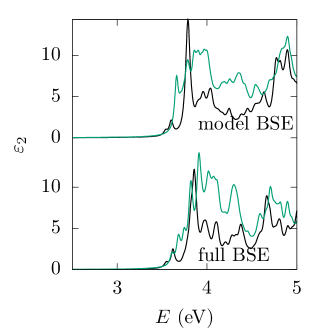
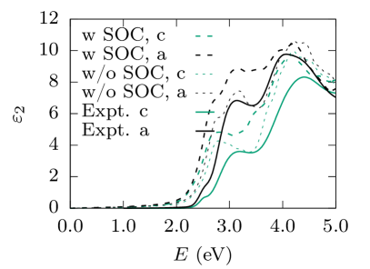
First, the calculated optical spectrum of the pristine bulk crystal is compared with the experimentally measured one. Figure 1 shows the imaginary part of the relative high-frequency dielectric permittivity (left axis) and the absorption coefficient (right axis). The calculated spectrum was obtained on LSDA+ level (=5.3 eV) in the IPA and averaged over the cartesian directions. This approach is used below for the optical spectra of BiFeO3 with defects.
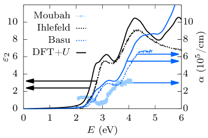
The calculated spectra on the independent-particle level are reasonably close to the experimentally measured ones of Refs. [Ihlefeld et al., 2008; Basu et al., 2008]. The underestimation of the quasiparticle gap and the missing excitonic binding energy and spin-orbit coupling largely cancel each other, except for a moderate redshift of eV. The spectrum from Ref. Moubah et al. (2012) appears blueshifted by about 0.5 eV. It should be noted that a larger Hubbard would increase the optical gap in the independent-particle approximation and hence move it closer to experiment Lima (2020); Ju et al. (2009), whereas including spin-orbit coupling would decrease the gap again Lima (2020). Considering that a larger value might overestimate the localization of electrons, a moderate of 5.3 eV, which yields simultaneously formation energies, band gaps, and ferroelectric polarization close to experiment (see Supplemental Material of Ref. [Körbel and Sanvito, 2020]), seems a safer choice for modeling polarons.

Figure 2 shows for the ordinary ( to the axis of the hexagonal unit cell) and extraordinary () axes of BiFeO3 from ellipsometry Choi et al. (2011), the IPA on the LSDA+ level (=6 eV), the IPA on the level, and from the BSE@. The shoulder at the absorption onset is less pronounced in the calculated spectra on the LSDA+ level than in experiment, on the -IPA level a shoulder is clearly visible. The magnitude of the shoulder depends on the broadening, the Hubbard , and the pseudopotential (see Figs. 1, 6, 10, and 11 in the Supplemental Material Note (1)). The BSE spectra are possibly not sufficiently converged with respect to -points in order to resolve a shoulder, but the model BSE with more -points yields a similar feature, see Fig. 12 in the Supplemental Material Note (1).
Figure 3 shows the transition charge densities weighted with the dipole matrix element of the hole and electron states forming the lowest optical transition () in the BSE,
| (3) |
and analogously for the hole, where is the coupling coefficient for the BSE eigenvalue , so Rohlfing and Louie (2000); Onida et al. (2002) and the excitonic wave function Rohlfing and Louie (2000), where and are the positions of electrons and holes. The indices , , and denote valence bands, conduction bands, and -points in the first Brillouin zone. The transition densities were calculated using PSP0.
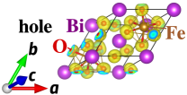
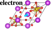

The lowest transition from hybridized O- and Fe- states to Fe- states (Fig. 3) should be partially dipole- and spin-forbidden Pisarev et al. (2009), so its oscillator strength would be underestimated in a calculation without spin-orbit coupling, as performed here. Self-consistency in , not considered here, might further modify the calculated spectral weight at the onset.
III.2 Optical spectra of BiFeO3 with defects
III.2.1 Absorption
Optical spectra of BiFeO3 with defects were calculated using the independent-particle approximation on the LSDA+ level (=5.3 eV) validated in the previous section.
Polarons.
Previous first-principles calculations indicate that excess electrons spontaneously form small polarons Körbel et al. (2018); Radmilovic et al. (2020), whereas holes form large polarons Körbel et al. (2018); Geneste, Grégory and Paillard, Charles and Dkhil, Brahim (2019). The large hole polaron occupies a metal-like state at the top of the valence band, whereas the small electron polaron occupies a midgap state such that the system retains a finite band gap Körbel et al. (2018); Radmilovic et al. (2020). Figure 4 shows the atomic configuration of the 71° domain wall and isosurfaces of the charge densities of excess electrons and holes.
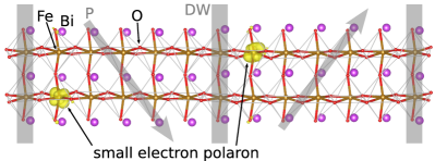
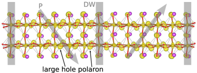
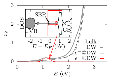
Figure 5 schematically shows the transitions involved in absorption and emission for pristine BiFeO3 and BiFeO3 with small electron polarons as an example for a defect with a deep level.
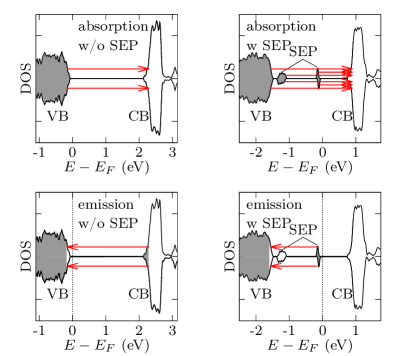
Figure 6 shows the optical spectra (imaginary part of the high-frequency relative dielectric permittivity , ) of BiFeO3 without (bulk) and with defects, and the difference between them ().
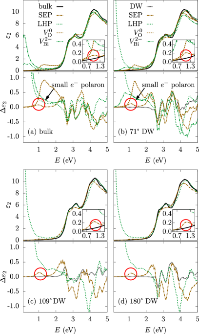
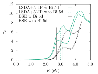
The optical spectrum of the pristine domain wall is nearly identical to that of the bulk. The large hole polaron leads to large absorption at vanishing photon energy due to its metallic density of states (Drude peak). In the case of the small electron polaron, instead an absorption peak is found at a photon energy of 1 eV, which is well separated in energy from the band edges, so the system remains insulating or semiconducting. For better visibility of the polaron peaks also the differential spectra () are shown in the bottom panels of Fig. 6. The small electron polaron peak is composed of electronic transitions between the small electron polaron level and the lowest conduction bands, as depicted in Fig. 7, which shows around the small polaron peak, the electronic density of states, and the contribution to that stems only from electronic transitions between the polaron level just below 0 eV and the lowest conduction bands near 1 eV (within the red rectangle). The electronic density of states of BiFeO3 with small electron polarons is in close agreement with that found in Ref. [Radmilovic et al., 2020].
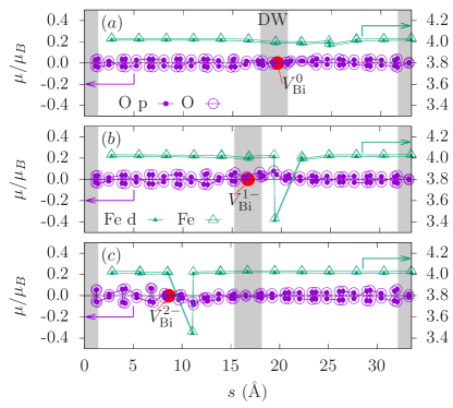
The spectra with oxygen vacancies also contain states within the gap, in agreement with Ref. [Radmilovic et al., 2020]. Transitions involving this localized electronic state near an oxygen vacancy appear to have an oscillator strength larger than that of the electron polaron in the bulk. In the case of bismuth vacancies near domain walls, the calculated local magnetic moments of Fe indicate that holes localize on Fe, forming Fe4+, see Fig. 8. Formation of Fe4+ near Bi vacancies at domain walls was also reported in Ref. [Rojac et al., 2017] based on spatially resolved electron-energy loss spectroscopy.
The spectra of the 109° and 180° domain walls are similar to that of the 71° wall. The most pronounced effects of the domain walls are the additional absorption peaks stemming from the defects located there. The oscillator strength of transitions involving defects is already small at the high doping level of the order of 1020–1021/cm3 considered here, and should decrease linearly for lower doping levels. Therefore, these defect signatures will be difficult to detect in absorption spectroscopy, but should be easier to find using photoluminescence spectroscopy (Kasha’s rule).
III.2.2 Photoluminescence
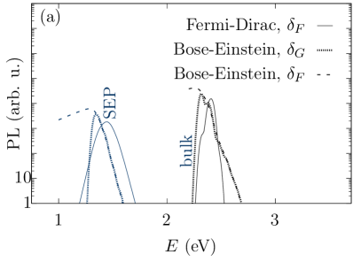
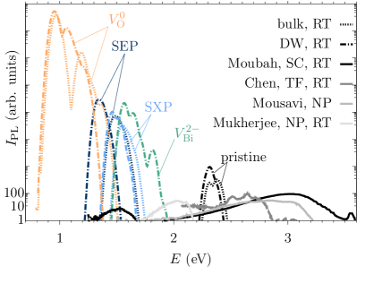
Figure 9 shows calculated PL spectra of the bulk and the 71° domain walls without and with defects together with experimental data. Other than in the case of the absorption spectra, the defect peaks deep inside the gap are no longer weak, even though here, other than for the absorption spectra above, a low defect concentration of the order of 1011/cm3 (excess electrons, oxygen vacancies) and 1015/cm3 (Bi vacancies) is assumed. The differences between bulk and domain walls and between electron and exciton polarons are subtle. It appears that the energy levels of the small electron polaron, the small exciton polaron, and the electrons at the oxygen vacancy are slightly lower at the domain wall than in the bulk, confirming that the domain walls act as traps for these defects. Like in the absorption spectra, the oscillator strengths of the transitions of electrons at oxygen vacancies are larger than those for electrons in bulk, otherwise the properties (energy level and shape of the wave function) of small electron polarons at oxygen vacancies Radmilovic et al. (2020) appear to be quite similar to those of small electron polarons in bulk or at domain walls, indicating that the properties of the small electron polaron may be largely independent of the nature of the electron trap. In the case of the Bi vacancy, it appears that if it is located near a domain wall, it can create a mid-gap level with a separate peak in emission. The differences in peak position, width, and shape between measured and calculated photoluminescence spectra should arise from neglect of electron-phonon interaction, from the band gap underestimation by LSDA+, and possibly from a non-thermal carrier distribution in experiment. Note that the exact shape of the calculated spectra, such as their tail at the onset, is sensitive to the type of broadening that was applied in the calculation (see Fig. 23 in the Supplemental Material Note (1).) We can conclude that (a) partial thermalization of the excited charge carriers should make it possible to detect the defect levels in photoluminescence, and (b) electron polarons, electrons at oxygen vacancies, and holes at Bi vacancies located at domain walls may have similar signatures and could be difficult to distinguish. If both the oxygen vacancy and the isolated electron polaron are present in similar concentrations, the peak of the oxygen vacancy should be dominant. The predicted photoluminescence spectra could be experimentally verified or falsified by performing photoluminescence spectroscopy of samples that have been prepared to contain a high concentration of domain walls and a specific point defect, which could be achieved by means of substrate strain (domain walls) and an oxygen-poor environment (oxygen vacancies) or by ensuring a Bi deficiency during processing (Bi vacancies).
IV Summary and Conclusions
Pristine BiFeO3.
The optical absorption spectrum of BiFeO3 calculated on the BSE@ level, using pseudopotentials and starting from LSDA+, is in close agreement with experiment,
but different choices of pseudopotentials and different numbers of frequencies in the part can change the calculated gap by several tenths of an eV.
A quasiparticle band gap of 3.1 eV and an optical band gap of 2.9 eV are obtained (excitonic binding energy 0.2 eV).
Due to partial cancellation of errors, the independent-particle approximation on LSDA+ level has a similar accuracy.
The agreement with experiment is best for eV.
Assuming that the methodology adopted here is valid, the shoulder at
the absorption onset cannot be explained by defect states, such as
those at oxygen vacancies, because the defect states lie too deep in
the gap so they form separate peaks rather than a shoulder.
Moreover, the defect concentration would need to be quite large (of the order of /cm3)
to give rise to a sizable signal in the absorption spectrum.
The shoulder is already present in calculated absorption spectra of defect-free BiFeO3.
It seems, therefore, more likely that the shoulder is composed of transitions between hybridized O-/Fe- valence states and Fe- conduction states
of pristine BiFeO3. Such transitions that are partially dipole- and spin-forbidden are likely underestimated by the methodology adopted here.
To validate the adopted methodology and to clarify the origin of the shoulder unambigously,
self-consistency in and a dense -point mesh using e.g. interpolation should be employed,
taking into account spin-orbit coupling, ideally also avoiding the use of pseudopotentials, a formidable task.
BiFeO3 with defects.
Different point defects, namely, electron polarons, electrons at oxygen vacancies, and possibly holes near bismuth vacancies apparently introduce defect states deep within the gap. These defect states seem to be at similar energies and may be difficult to distinguish. In the case of hole doping (-type conditions), a Drude peak should appear due to the metal-like density of states of the large hole polaron. The spectroscopic signatures of the point defects should only be visible in absorption spectra at high defect concentrations of the order of 1020/cm3, whereas they should be visible in photoluminescence at lower concentrations, such as 1011/cm3, provided the excited carriers are near thermal equilibrium and their concentration is of the order of the defect concentration or lower, otherwise bulk transitions should dominate. The ferroelectric domain walls seem to accumulate these point defects rather than to affect the spectra directly.
Acknowledgement
S. K. thanks F. Bechstedt, S. Botti, J. Hlinka, and S. Sanvito for helpful discussion, P. Ghosez for pointing out literature, and S. Choi for sharing ellipsometry data. This project has received funding from the European Union’s Horizon 2020 research and innovation programme under the Marie Skłodowska-Curie Grant Agreement No. 746964. Computational resources and support were supplied by the Trinity Centre for High Performance Computing funded by Science Foundation Ireland, by the Irish Centre for High-End Computing, and and by the e-INFRA CZ project (ID:90254), supported by the Ministry of Education, Youth and Sports of the Czech Republic, and the HPC cluster ARA of the University of Jena, Germany. Figures were made using Vesta Momma and Izumi (2011) and gnuplot.
References
- Lebeugle et al. (2007) Delphine Lebeugle, Dorothée Colson, A Forget, and Michel Viret, “Very large spontaneous electric polarization in BiFeO3 single crystals at room temperature and its evolution under cycling fields,” Appl. Phys. Lett. 91, 022907 (2007).
- Smolenskii and Chupis (1982) G A Smolenskii and I E Chupis, “Ferroelectromagnets,” Sov. Phys. Usp. 25, 475–493 (1982).
- Basu et al. (2008) S. R. Basu, L. W. Martin, Y. H. Chu, M. Gajek, R. Ramesh, R. C. Rai, X. Xu, , and J. L. Musfeldt, “Photoconductivity in BiFeO3 thin films,” Appl. Phys. Lett. 92, 091905 (2008).
- Hauser et al. (2008) A. J. Hauser, J. Zhang, L. Mier, R. A. Ricciardo, P. M. Woodward, T. L. Gustafson, L. J. Brillson, and F. Y. Yang, “Characterization of electronic structure and defect states of thin epitaxial BiFeO3 films by UV-visible absorption and cathodoluminescence spectroscopies,” Appl. Phys. Lett. 92, 222901 (2008).
- Ihlefeld et al. (2008) JF Ihlefeld, NJ Podraza, ZK Liu, RC Rai, X Xu, T Heeg, YB Chen, J Li, RW Collins, JL Musfeldt, et al., “Optical band gap of BiFeO3 grown by molecular-beam epitaxy,” Appl. Phys. Lett. 92, 142908 (2008).
- Kumar et al. (2008) Amit Kumar, Ram C Rai, Nikolas J Podraza, Sava Denev, Mariola Ramirez, Ying-Hao Chu, Lane W Martin, Jon Ihlefeld, T Heeg, J Schubert, et al., “Linear and nonlinear optical properties of BiFeO3,” Appl. Phys. Lett. 92, 121915 (2008).
- Železný et al. (2010) V Železný, D Chvostová, L Pajasová, I Vrejoiu, and M Alexe, “Optical properties of epitaxial BiFeO3 thin films,” Applied Physics A 100, 1217–1220 (2010).
- Sando et al. (2018) Daniel Sando, Cécile Carrétéro, Mathieu N Grisolia, Agnès Barthélémy, Valanoor Nagarajan, and Manuel Bibes, “Revisiting the Optical Band Gap in Epitaxial BiFeO3 Thin Films,” Advanced Optical Materials 6, 1700836 (2018).
- Moubah et al. (2012) Reda Moubah, Guy Schmerber, Olivier Rousseau, Dorothée Colson, and Michel Viret, “Photoluminescence investigation of defects and optical band gap in multiferroic BiFeO3 single crystals,” Applied Physics Express 5, 035802 (2012).
- Fridkin (2001) V.M. Fridkin, “Bulk photovoltaic effect in noncentrosymmetric crystals,” Crystallogr. Rep. 46, 654–658 (2001).
- Choi et al. (2009) T. Choi, S. Lee, Y. J. Choi, V. Kiryukhin, and S.-W. Cheong, “Switchable Ferroelectric Diode and Photovoltaic Effect in BiFeO3,” Science 324 (2009).
- Ji et al. (2011) Wei Ji, Kui Yao, and Yung C. Liang, “Evidence of bulk photovoltaic effect and large tensor coefficient in ferroelectric BiFeO3 thin films,” Phys. Rev. B 84, 094115 (2011).
- Bhatnagar et al. (2013) Akash Bhatnagar, Ayan Roy Chaudhuri, Young Heon Kim, Dietrich Hesse, and Marin Alexe, “Role of domain walls in the abnormal photovoltaic effect in BiFeO3,” Nature communications 4, 2835 (2013).
- Goffinet et al. (2009) M. Goffinet, P. Hermet, D. I. Bilc, and Ph. Ghosez, “Hybrid functional study of prototypical multiferroic bismuth ferrite,” Phys. Rev. B 79, 014403 (2009).
- Stroppa and Picozzi (2010) A Stroppa and S Picozzi, “Hybrid functional study of proper and improper multiferroics,” Phys. Chem. Chem. Phys. 12, 5405–5416 (2010).
- Pisarev et al. (2009) R. V. Pisarev, A. S. Moskvin, A. M. Kalashnikova, and Th. Rasing, “Charge transfer transitions in multiferroic BiFeO3 and related ferrite insulators,” Phys. Rev. B 79, 235128 (2009).
- Choi et al. (2011) SG Choi, HT Yi, S-W Cheong, JN Hilfiker, R France, and AG Norman, “Optical anisotropy and charge-transfer transition energies in BiFeO3 from 1.0 to 5.5 eV,” Phys. Rev. B 83, 100101R (2011).
- Himcinschi et al. (2010) C Himcinschi, I Vrejoiu, M Friedrich, E Nikulina, L Ding, C Cobet, N Esser, M Alexe, D Rafaja, and DRT Zahn, “Substrate influence on the optical and structural properties of pulsed laser deposited BiFeO3 epitaxial films,” J. Appl. Phys. 107, 123524 (2010).
- Lima (2020) A F Lima, “Optical properties, energy band gap and the charge carriers’ effective masses of the BiFeO3 magnetoelectric compound,” Journal of Physics and Chemistry of Solids 144, 109484 (2020).
- Radmilovic et al. (2020) Andjela Radmilovic, Tyler J Smart, Yuan Ping, and Kyoung-Shin Choi, “Combined Experimental and Theoretical Investigations of n-Type BiFeO3 for Use as a Photoanode in a Photoelectrochemical Cell,” Chem. Mater. 32, 3262–3270 (2020).
- Ederer and Spaldin (2005) Claude Ederer and Nicola A. Spaldin, “Influence of strain and oxygen vacancies on the magnetoelectric properties of multiferroic bismuth ferrite,” Phys. Rev. B 71, 224103 (2005).
- Ju and Cai (2009) Sheng Ju and Tian-Yi Cai, “First-principles studies of the effect of oxygen vacancies on the electronic structure and linear optical response of multiferroic BiFeO3,” Appl. Phys. Lett. 95, 231906 (2009).
- Rojac et al. (2017) Tadej Rojac, Andreja Bencan, Goran Drazic, Naonori Sakamoto, Hana Ursic, Bostjan Jancar, Gasper Tavcar, Maja Makarovic, Julian Walker, Barbara Malic, et al., “Domain-wall conduction in ferroelectric BiFeO3 controlled by accumulation of charged defects,” Nat. Mater. 16, 322 (2017).
- Lohaus et al. (2018) Christian Lohaus, Andreas Klein, and Wolfram Jaegermann, “Limitation of Fermi level shifts by polaron defect states in hematite photoelectrodes,” Nat. Commun. 9, 1–7 (2018).
- Peng and Lany (2012) Haowei Peng and Stephan Lany, “Semiconducting transition-metal oxides based on d5 cations: Theory for MnO and Fe2O3,” Phys. Rev. B 85, 201202R (2012).
- Körbel et al. (2018) Sabine Körbel, Jirka Hlinka, and Stefano Sanvito, “Electron trapping by neutral pristine ferroelectric domain walls in ,” Phys. Rev. B 98, 100104(R) (2018).
- Geneste, Grégory and Paillard, Charles and Dkhil, Brahim (2019) Geneste, Grégory and Paillard, Charles and Dkhil, Brahim, “Polarons, vacancies, vacancy associations, and defect states in multiferroic BiFeO3,” Phys. Rev. B 99, 024104 (2019).
- Seidel et al. (2009) Jan Seidel, Lane W Martin, Q He, Q Zhan, Y-H Chu, A Rother, ME Hawkridge, P Maksymovych, P Yu, M Gajek, et al., “Conduction at domain walls in oxide multiferroics,” Nat. Mater. 8, 229–234 (2009).
- Guyonnet et al. (2011) Jill Guyonnet, Iaroslav Gaponenko, Stefano Gariglio, and Patrycja Paruch, “Conduction at domain walls in insulating Pb(Zr0.2Ti0.8)O3 thin films,” Advanced Materials 23, 5377–5382 (2011).
- Farokhipoor and Noheda (2011) S Farokhipoor and Beatriz Noheda, “Conduction through 71° domain walls in BiFeO3 thin films,” Phys. Rev. Lett. 107, 127601 (2011).
- Bencan et al. (2020) Andreja Bencan, Goran Drazic, Hana Ursic, Maja Makarovic, Matej Komelj, and Tadej Rojac, “Domain-wall pinning and defect ordering in BiFeO3 probed on the atomic and nanoscale,” Nat. Commun. 11, 1–9 (2020).
- Gaponenko et al. (2015) I Gaponenko, P Tückmantel, J Karthik, LW Martin, and P Paruch, “Towards reversible control of domain wall conduction in Pb(Zr0.2Ti0.8)O3 thin films,” Appl. Phys. Lett. 106, 162902 (2015).
- Kresse and Furthmüller (1996) Georg Kresse and Jürgen Furthmüller, “Efficiency of ab-initio total energy calculations for metals and semiconductors using a plane-wave basis set,” Comput. Mater. Sci. 6, 15–50 (1996).
- Dudarev et al. (1998) S. L. Dudarev, G. A. Botton, S. Y. Savrasov, C. J. Humphreys, and A. P. Sutton, “Electron-energy-loss spectra and the structural stability of nickel oxide: An LSDA+U study,” Phys. Rev. B 57, 1505–1509 (1998).
- Jain et al. (2013) Anubhav Jain, Shyue Ping Ong, Geoffroy Hautier, Wei Chen, William Davidson Richards, Stephen Dacek, Shreyas Cholia, Dan Gunter, David Skinner, Gerbrand Ceder, and Kristin A. Persson, “The Materials Project: A materials genome approach to accelerating materials innovation,” APL Materials 1, 011002 (2013), https://doi.org/10.1063/1.4812323.
- Körbel and Sanvito (2020) Sabine Körbel and Stefano Sanvito, “Photovoltage from ferroelectric domain walls in BiFeO3,” Phys. Rev. B 102, 081304(R) (2020).
- Sadigh et al. (2015) Babak Sadigh, Paul Erhart, and Daniel Åberg, “Variational polaron self-interaction-corrected total-energy functional for charge excitations in insulators,” Phys. Rev. B 92, 075202 (2015).
- Erhart et al. (2014) Paul Erhart, Andreas Klein, Daniel Åberg, and Babak Sadigh, “Efficacy of the DFT+U formalism for modeling hole polarons in perovskite oxides,” Phys. Rev. B 90, 035204 (2014).
- Franchini et al. (2021) Cesare Franchini, Michele Reticcioli, Martin Setvin, and Ulrike Diebold, “Polarons in materials,” Nature Reviews Materials , 1–27 (2021).
- Diéguez, Oswaldo and Aguado-Puente, Pablo and Junquera, Javier and Íñiguez, Jorge (2013) Diéguez, Oswaldo and Aguado-Puente, Pablo and Junquera, Javier and Íñiguez, Jorge, “Domain walls in a perovskite oxide with two primary structural order parameters: First-principles study of BiFeO3,” Phys. Rev. B 87, 024102 (2013).
- Ren et al. (2013) Wei Ren, Yurong Yang, Oswaldo Diéguez, Jorge Íñiguez, Narayani Choudhury, and L. Bellaiche, “Ferroelectric Domains in Multiferroic Films under Epitaxial Strains,” Phys. Rev. Lett. 110, 187601 (2013).
- Wang et al. (2013) Yi Wang, Chris Nelson, Alexander Melville, Benjamin Winchester, Shunli Shang, Zi-Kui Liu, Darrell G Schlom, Xiaoqing Pan, and Long-Qing Chen, “BiFeO3 domain wall energies and structures: a combined experimental and density functional theory+U study,” Phys. Rev. Lett. 110, 267601 (2013).
- Chen et al. (2017) Yun-Wen Chen, Jer-Lai Kuo, and Khian-Hooi Chew, “Polar ordering and structural distortion in electronic domain-wall properties of BiFeO3,” J. Appl. Phys. 122, 075103 (2017).
- Fousek and Janovec (1969) Jan Fousek and Václav Janovec, “The orientation of domain walls in twinned ferroelectric crystals,” J. Appl. Phys. 40, 135–142 (1969).
- Note (1) See Supplemental Material at http://link.aps.org/supplemental/10.1103/PhysRevMaterials.7.104402 for a validation of the computational methods, fits, and additional computational details .
- Bokdam et al. (2016) Menno Bokdam, Tobias Sander, Alessandro Stroppa, Silvia Picozzi, DD Sarma, Cesare Franchini, and Georg Kresse, “Role of polar phonons in the photo excited state of metal halide perovskites,” Sci. Rep. 6, 1–8 (2016).
- Varrassi et al. (2021) Lorenzo Varrassi, Peitao Liu, Zeynep Ergönenc Yavas, Menno Bokdam, Georg Kresse, and Cesare Franchini, “Optical and excitonic properties of transition metal oxide perovskites by the Bethe-Salpeter equation,” Phys. Rev. Materials 5, 074601 (2021).
- Qiu et al. (2013) Diana Y. Qiu, Felipe H. da Jornada, and Steven G. Louie, “Optical Spectrum of : Many-Body Effects and Diversity of Exciton States,” Phys. Rev. Lett. 111, 216805 (2013).
- Gajdoš et al. (2006) M Gajdoš, K Hummer, G Kresse, J Furthmüller, and F Bechstedt, “Linear optical properties in the projector-augmented wave methodology,” Phys. Rev. B 73, 045112 (2006).
- Jackson (1999) John David Jackson, Classical Electrodynamics (John Wiley & Sons, New Jersey, 1999).
- Albert Einstein (1917) Albert Einstein, “Zur Quantentheorie der Strahlung [On the quantum theory of radiation],” Physik. Zeitschr. 18, 121–128 (1917).
- Cardona and Yu (2010) Manuel Cardona and Peter Y Yu, Fundamentals of semiconductors, 4th ed. (Springer, Berlin Heidelberg, 2010).
- Hannewald et al. (2000) K Hannewald, S Glutsch, and F Bechstedt, “Theory of photoluminescence in semiconductors,” Phys. Rev. B 62, 4519 (2000).
- cof (2022) https://github.com/skoerbel/cofimaker (2022).
- Torun et al. (2018) Engin Torun, Henrique PC Miranda, Alejandro Molina-Sánchez, and Ludger Wirtz, “Interlayer and intralayer excitons in MoS2/WS2 and MoSe2/WSe2 heterobilayers,” Phys. Rev. B 97, 245427 (2018).
- Cannuccia et al. (2019) E. Cannuccia, B. Monserrat, and C. Attaccalite, “Theory of phonon-assisted luminescence in solids: Application to hexagonal boron nitride,” Phys. Rev. B 99, 081109R (2019).
- Ju et al. (2009) Sheng Ju, Tian-Yi Cai, and Guang-Yu Guo, “Electronic structure, linear, and nonlinear optical responses in magnetoelectric multiferroic material BiFeO3,” The Journal of Chemical Physics 130, 214708 (2009), https://doi.org/10.1063/1.3146796 .
- Rohlfing and Louie (2000) Michael Rohlfing and Steven G Louie, “Electron-hole excitations and optical spectra from first principles,” Phys. Rev. B 62, 4927 (2000).
- Onida et al. (2002) Giovanni Onida, Lucia Reining, and Angel Rubio, “Electronic excitations: density-functional versus many-body Green’s-function approaches,” Rev. Mod. Phys. 74, 601 (2002).
- Chen et al. (2012) Xinman Chen, Hu Zhang, Tao Wang, Feifei Wang, and Wangzhou Shi, “Optical and photoluminescence properties of BiFeO3 thin films grown on ITO-coated glass substrates by chemical solution deposition,” Phys. Status Solidi A 209, 1456–1460 (2012).
- Mukherjee et al. (2018) Ayan Mukherjee, Sankalpita Chakrabarty, Neetu Kumari, Wei-Nien Su, and Suddhasatwa Basu, “Visible-light-mediated electrocatalytic activity in reduced graphene oxide-supported bismuth ferrite,” ACS Omega 3, 5946–5957 (2018).
- Mousavi Ghahfarokhi et al. (2022) Seyed Ebrahim Mousavi Ghahfarokhi, Khadijeh Helfi, and Morteza Zargar Shoushtari, “Synthesis of the Single-Phase Bismuth Ferrite (BiFeO3) Nanoparticle and Investigation of Their Structural, Magnetic, Optical and Photocatalytic Properties,” Advanced Journal of Chemistry-Section A 5, 45–58 (2022).
- Momma and Izumi (2011) Koichi Momma and Fujio Izumi, “VESTA3 for three-dimensional visualization of crystal, volumetric and morphology data,” J. Appl. Crystallogr. 44, 1272–1276 (2011).
Supplemental Information
Optical signatures of defects in BiFeO3
I Convergence tests for bulk BiFeO3
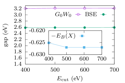
This section contains convergence tests for the 10-atom unit cell of perfect rhombohedral BiFeO3. Details of the pseudopotentials (PSP) used and calculation results are given in Table 4. Where not stated otherwise, test calculations were carried out with a plane-wave cutoff energy eV, a cutoff energy for the dielectric permittivity =300 eV, and a -point grid, 1560 bands in total, of which bands were corrected with , neglecting spin-orbit coupling.
I.1 -points
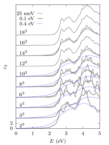
Figure 10 shows obtained in the independent particle approximation (IPA) on LSDA+ level (=5.3 eV) using PSP0 for different -point meshes ( to ) and different spectral broadenings (25 meV to 0.4 eV). The -point convergence depends on the broadening: For 25 meV a dense mesh of -points is needed, for 0.4 eV a mesh of -points already yields nearly converged spectra.
The -point convergence of the BSE spectra is shown in section I.8.
I.2 Number of frequencies in
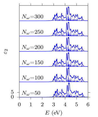
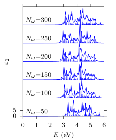
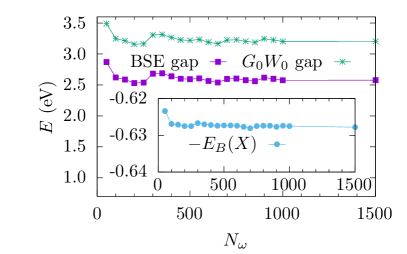
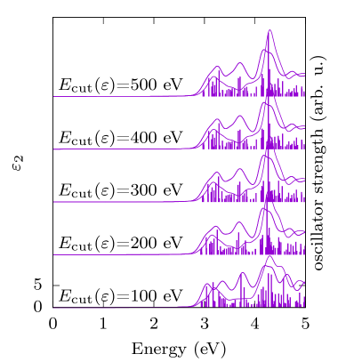
Figure 11 shows (broadened by 0.1 eV) and the oscillator strengths from the BSE@ as a function of the number of frequencies in , using PSP1 and PSP2, =6 eV, and 16 valence and 16 conduction bands in the BSE. Figure 12 shows the gaps from and the BSE as well as the exciton binding energy. The exciton binding energy and the spectral shape are approximately converged at 100. The gaps themselves converge more slowly and still vary by 0.1 eV above 100.
I.3 Total number of bands
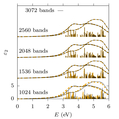
Figure 13 shows (broadened by 0.4 eV) and the oscillator strengths from the BSE@ as a function of the total number of bands included in the part using eV, PSP0, eV, , and 8 valence and 8 conduction bands in the BSE. Using 1560 bands all transition energies up to 5.7 eV are converged within 40 meV compared to the calculation with 3072 bands. For 2048 bands all transition energies up to 6 eV are converged within 3 meV.
I.4 Number of bands in the BSE
Figure 14 shows (broadened by 0.4 eV) and the oscillator strengths from the BSE@ as a function of the number of valence and conduction bands (VB and CB) included in the BSE part, using =5.3 eV, PSP0, , and eV. The spectra obtained with 12 VB and 12 CB are already identical to those obtained with 20 VB and 20 CB.

I.5 Hubbard
Figure 15 shows (broadened by 25 meV) on LSDA+ level as a function of the Hubbard , using PSP2, 120 bands, and a -point grid. The best agreement with experiment is obtained for 6 eV.
Figure 16 shows the Kohn-Sham (LSDA+), , and BSE@ gaps as a function of the Hubbard , using PSP2, a -point grid, , and 16 valence and 16 conduction bands in the BSE. Both the gaps and the exciton binding energy depend considerably on the starting point, i. e. the parameter.
I.6 Plane wave energy cutoff
Fig. 17 shows the and BSE@ gaps and the exciton binding energy as a function of the cutoff energy of the basis functions , using PSP1 and PSP2, =6 eV, , eV, and 16 valence and 16 conduction bands in the BSE. The gaps and exciton binding energies are converged at eV.
I.7 Energy cutoff for
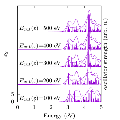
Fig. 18 shows the and BSE@ gaps and the exciton binding energy as a function of the cutoff energy of the dielectric matrix , using PSP1 and PSP2, =6 eV, , and 16 valence and 16 conduction bands in the BSE. The gaps are converged at eV (PSP1) and eV (PSP2), respectively.
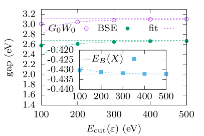
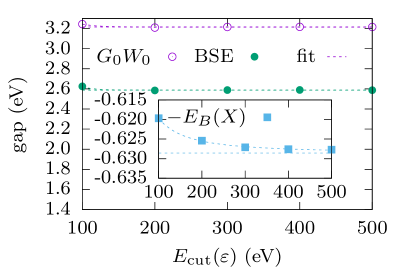
Fig. 19 shows (broadened by 0.1 eV) and the oscillator strengths for different using PSP1 and PSP2. The shape of the spectra and the oscillator strengths of the transitions near the onset are converged at 200 eV.
I.8 model BSE
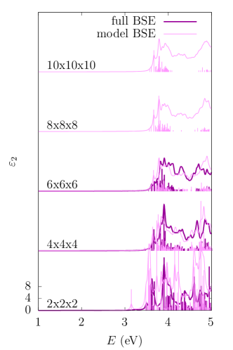
Figure 20 shows from the model BSE (mBSE@LSDA++scissor) as a function of the -point mesh in comparison with the full BSE@ obtained with PSP1 and PSP2, using =6 eV and a -point grid. For the full BSE and eV were used. Both the model and the full BSE were solved for 16 valence and 16 conduction bands. Figure 21 shows the convergence of full and model BSE with -points. Figure 22 shows the gaps obtained from the model BSE in comparison with BSE@.


I.9 Spin-orbit coupling
Figure 23 shows (broadened by 0.1 eV) on LSDA+ level obtained with and without including spin-orbit coupling (SOC), using PSP0, =5.3 eV, 100 bands, and an -point grid. SOC has a considerable effect on the optical absorption spectra and should therefore be included in the calculation. However, since inclusion of SOC doubles the computation time, reduces the band gap only by 0.1 eV, and does not clearly improve the agreement with experimental spectra, it is neglected in the supercell calculations with defects. Neglecting spin-orbit coupling partially cancels the band gap underestimation of LSDA+ with =5.3 eV.
I.10 Local field effects
Figure 24 shows (broadened by 0.1 eV) on LSDA+ level (=5.3 eV) obtained with and without local field effects (LFE), using PSP0 and 50 bands. The local field effects reduce the spectral weight for energies up to 5 eV by about 10%.

I.11 Bi semicore electrons
Figure 25 shows obtained with and without including Bi semicore electrons in the valence, using PSP0 (with “Bi-d” instead of “Bi” in the case of semicore included), =5.3 eV, and 100 bands. The spectra for light polarization along the principle axes were calculated with LSDA on the independent-particle level, neglecting local-field effects, for an -point mesh and a broadening of 0.1 eV, and with the BSE@ on a -point mesh, broadened by 0.4 eV. The contribution of the electrons of Bi to the optical absorption spectra on LSDA+ level near the absorption onset is negligible, but the gap is affected by the Bi semicore electrons.
I.12 pseudopotentials
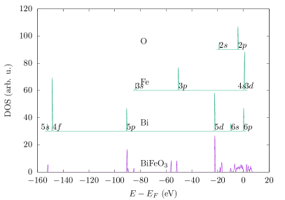
Figure 26 shows the atomic states involved in the electronic structure of BiFeO3. The states of Bi are missing in the depicted density of states of BiFeO3 because in the pseudopotential they are part of the core electrons. Two pseudopotentials with energetically well-separated core and valence states were finally chosen for the calculations, namely the “Bi-d Fe O” (15, 8, and 6 valence electrons) and the “Bi-sv-GW, Fe-sv-GW, O-GW” (23, 16, and 6 valence electrons) sets.
Different pseudopotentials yield different gaps, especially on the level. The BSE gaps are less sensitive to the pseudopotential. Figure 27 shows the gaps on LSDA+ (=5.3 eV), , and BSE@ level for different pseudopotentials, using =150.
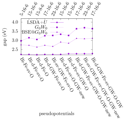
The gaps vary between 3.0 and 3.6 eV, the BSE gaps between 2.6 and 3.1 eV, the exciton binding energy between 0.2 and 0.6 eV. Within the pseudopotential approach, as adopted here, it appears difficult to obtain more than a lower limit for the gap. Figure 28 shows on LSDA+ level (=5.3 eV, 0.2 eV broadening) obtained with different pseudopotentials. Except for the pseudopotential without Fe semicore (“Bi-d-Fe-O”) all spectra are nearly identical on LSDA+ level.

Figure 29 shows (broadened by 0.4 eV) from the BSE@ obtained with different pseudopotentials. The spectrum onset and the shape of the extraordinary component vary with the pseudopotential.
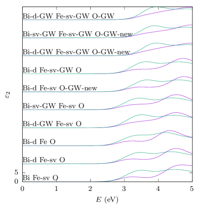
| “Bi Fe-sv O” (PSP0) | “Bi-d Fe O” (PSP1) | “Bi-sv-GW Fe-sv-GW O-GW” (PSP2) | |
| valence conf. | Bi | Bi | Bi |
| Fe | Fe | Fe | |
| O | O | O | |
| LSDA+ gap w/o SOC | dir. 2.35, fund. 2.30 | dir. 2.36 , fund. 2.36 | dir. 2.41, fund. 2.36 |
| LSDA+ gap w SOC | dir. 2.25, fund. 2.19 | dir. 2.25, fund. 2.25 | dir. 2.31, fund. 2.26 |
| corr. (SOC) | dir. -0.11, fund. -0.11 | dir. -0.10, fund. -0.11 | dir. -0.10, fund. -0.11 |
| corr (()) | +0.03 | 0.00 | |
| corr. (BSE -points) | 0.04 | 0.05 | |
| dir. gap (uncorr.) | 3.13 (3.20) | 3.67 (3.77) | |
| fund. gap (uncorr.) | 3.08 (3.16) | 3.57 (3.68) | |
| BSE gap (uncorr.) | 2.92 (2.95) | 3.5 (3.54) | |
| 0.21 | 0.21 | ||
| scissor | 0.84 eV | 1.36 eV | |
| 7.26 | 7.25 | ||
| 1.417 | 1.470 |
I.13 Dipole matrix elements
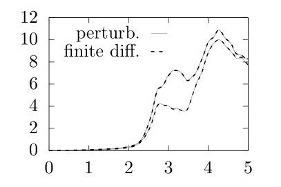
Figure 30 shows (broadened by 0.1 eV) on LSDA+ level (=5.3 eV, using PSP0 and -points) obtained with dipole matrix elements from perturbation theory and from finite differences, respectively. The differences are negligible.
I.14 Tamm-Dancoff approximation
Figure 31 shows (broadened by 0.4 eV) obtained at the BSE@ level with and without the Tamm-Dancoff approximation (TDA), using =5.3 eV, PSP0, =75, eV, and 8 valence and 8 conduction bands in the BSE. The differences due to the TDA are negligible.

Summary
Approximately converged exciton binding energies can be obtained with the calculation parameters in Table 5.
| parameter | converged at |
|---|---|
| 500 eV | |
| -mesh | points (better ) |
| BSE -mesh | points (better ) |
| 100 (better 150) | |
| total # of bands in | 1536 (better 2048) |
| 200 eV | |
| # of BSE bands | 8 VB, 8 CB (better 12 VB, 12 CB) |
| SOC | included |
| local field effects | included |
| antiresonant terms | TDA |
The (BSE@) gaps in the main text were corrected for spin-orbit coupling and extrapolated to an infinite cutoff energy of the dielectric matrix, and to an infinitely dense -point mesh (only BSE).
II Tests for domain walls
This section contains convergence tests for the 120-atom cell of BiFeO3 with 71° domain walls.
II.1 Excitons vs. independent particles in PL spectra
While the absorption spectra of domain walls were calculated in the independent-particle approximation, in the photoluminescence spectrum excitons were introduced afterwards by weighting the absorption spectrum with a Bose-Einstein distribution. Figure 32 shows the photoluminescence spectrum from this approach in comparison with that from a thermal distribution of independent electrons and holes. Differences in the spectra arise due to the difference between Bose and Fermi distribution and different approximations of the function in Eq. (1) in the main text: A Gaussian, , was tested as well as a Fermi function derivative, , .