Topological phase transition in a narrow bandgap semiconductor nanolayer
Abstract
Narrow bandgap semiconductor nanostructures have been explored for realization of topological superconducting quantum devices in which Majorana states can be created and employed for constructing topological qubits. However, a prerequisite to achieve the topological phase transition in these nanostructures is application of a magnetic field, which could complicate the technology development towards topological quantum computing. Here we demonstrate that a topological phase transition can be achieved in a narrow bandgap semiconductor nanolayer under application of a perpendicular electric field. Based on full band structure calculations, it is shown that the topological phase transition occurs at an electric-field induced band inversion and is accompanied by a sharp change of the invariant at the critical field. We also demonstrate that the nontrivial topological phase is manifested by the quantum spin Hall edge states in a band-inverted nanolayer Hall-bar structure. We present the phase diagram of the nanolayer in the space of layer thickness and electric field strength, and discuss the optimal conditions to achieve a large topological bandgap in the electric-field induced topological phase of a semiconductor nanolayer.
Introduction.—Recently, narrow bandgap semiconductor nanostructures have attracted intensive attentions for exploring new topological phases of matter Qi2011 ; Frolov2020 ; Hasan2010 ; Lutchym2018 . Free-standing narrow bandgap semiconductor InAs and InSb nanowires can be made in proximity to -wave superconductors to create zero-energy Majorana bound states (MBSs) due to the intrinsic strong spin-orbit couplings (SOCs) in the materials Lutchyn2010 ; Oreg2010 . Although the signatures of single MBSs have been detected in semiconductor-superconductor heterostructured nanowires in recent years Mourik2012 ; Deng2012 ; Deng2016 ; Aghaee2023 , it is still experimentally challenging to integrate two or more pairs of MBSs together in these one-dimensional (1D) systems for implementing topological quantum computing Alicea2011 ; Aasen2016 ; Aguado2020 ; Sarma2015 . By assuming the coexistence of superconductivity and topological order in a two-dimensional (2D) topological insulator (TI), it is theoretically predicted that the creation and manipulation of topological qubits can be realized Fu2008 ; Schulz2020 ; Heck2015 ; Guo2023 ; Lian2018 . However, conventional narrow bandgap semiconductor layers, such as free-standing InAs and InSb nanolayers Mata2016 ; Pan2016 ; Pan2019 , with good superconducting proximity effects and strong SOCs, have usually but widely exploited in their trivial phase Zhi2019 ; Kang2019 ; Chen2021 ; Zhang2022 ; Fan2022 ; Zhang2022-2 ; Yan2023 . Thus, it is fundamentally important to show whether a nontrivial topological phase can be induced into these conventional layered semiconductor materials using an experimentally accessible, controlled method.
Here, in this article, we propose a new but experimentally convenient way of introducing a 2D TI phase in a planar narrow bandgap semiconductor nanolayer. We will demonstrate that a perpendicular electrical field can be employed to manipulate the energy bands and to induce a topological phase transition in the semiconductor nanolayer. Experimentally, application of such a perpendicular electrical field to a semiconductor nanolayer can be achieved via a planar dual-gate technique Chen2021 ; Zhang2022 ; Fan2022 . The demonstration is based on solid calculations for the full band structures and the invariant of a typical semiconductor, such as an InSb nanolayer, under different strengths of the applied electrical field. We will show that the energy bands will be inverted, when the electrical field becomes larger than a critical strength, and the nanolayer will undergo a sharp topological phase transition under tuning of the electrical field through the critical field. We will also present the phase diagram of the nanolayer from which a guideline of finding optimal conditions to achieve a large topological bandgap can be extracted.
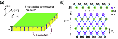
Band inversion and topological phase transition.—To demonstrate the principal concept, we consider an InSb nanolayer with a finite thickness but with infinite planar dimensions under application of a perpendicular electric field [as indicated in the schematic of Fig. 1(a)]. Thus, the nanolayer can be effectively viewed as a 2D lattice with the size of a unit cell proportional to the layer thickness. The 2D band structures are calculated under different strengths of the electric field and the topological phase transition are analyzed by examining the electric-field induced variation of the bandgap and the characteristic topological invariant. The renowned tight binding (TB) method Vogl1983 is adopted in the calculations of the band structures and the normal direction of the layer is assumed to be parallel to the crystallographic [001] direction. The obtained results can be straightforwardly extended to the layers with different normal crystallographic directions.
Expanding in the basis Vogl1983 , the Hamiltonian of the system can be written as,
| (1) |
where represents spin-orbital basis state at , is a lattice vector, is the displacement of atom in a unit cell, and is an in-plane wave vector with and being defined along the crystallographic [1-10] and [110] directions. The diagonal terms in Eq. (1) represent the on-site atomic orbital energies, while the off-diagonal terms describe the interactions between different intra-atomic orbitals, i.e., the terms arising from the intrinsic SOCs between the intra-atomic orbitals, and the interactions between nearest-neighbor atomic orbitals Persson2006 ; Liao2016 ; SM . The effect of the external electric field is taken into consideration by adding a location-dependent electric potential to the on-site energies Xiao2019 ,
| (2) |
where is the elementary charge, represents the electric field strength, the indices of the atomic layers, an offset constant, and the inter-atomic layer distance with denoting the material lattice constant and giving the thickness of the nanolayer [see Fig. 1(a)]. In order to avoid the effect of surface relaxation and reconstruction on the calculations, the dangling bonds of the surface atoms have been passivated by hydrogen-like atoms Persson2006 ; Liao2016 ; SM . For further details and the TB parameters employed in the calculations for the band structures of InSb nanolayers with hydrogen passivated surfaces, we refer to Ref. SM, .
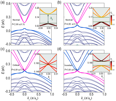
To illustrate the bandgap variation with the external perpendicular electric field and the topological phase transition in a semiconductor nanolayer, we show in Fig. 2 the calculated band structures of the InSb nanolayer with at different electric field strengths . Figure 2(a) shows the energy band structure at a small electric field, where is the bandgap at the point. As depicted in Figs. 2(b) and 2(c), the bandgap is reduced with increasing and gets closed when the field reaches to a critical value of mV/Å. With further increasing , the conduction and valence bands will be inverted and the electron-hole hybridization promotes a bandgap reopening, as demonstrated in Fig. 2(d). The band inversion can also be manifested by changes in the orbital characters of the Bloch bands near the bandgap SM . When goes beyond the critical field, the bands below and above the bandgap contain contributions dominantly from the - and -like orbitals, respectively, which is opposite to that in the normal, no-band-inversion cases [see the insets of Fig. 2].
For 2D Bloch bands with time-reversal symmetry, the topology is characterized by a single invariant Hasan2010 ; Qi2011 , with two possibly taking values of 0 and 1, and the nonzero invariant corresponds to the nontrivial phase. The determination of the invariant involves all the occupied Bloch bands over the half Brillouin zone (BZ) Fu2006a , and the breaking of the inversion symmetry induced by the perpendicular electric field complicates the calculations for the values of the invariant. However, by regarding one component of the 2D wave vector as an virtual periodic time parameter, the invariant can be ascertained by tracking the evolutions of the centers of maximum localized Wannier functions, constructed from the fully occupied bands, over a half period Soluyanov2011 ; Yu2011 ; SM .
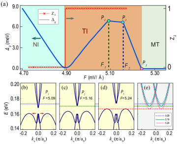
Figure 3(a) shows the derived topological invariant and the bandgap as a function of the electric field for the InSb nanolayer with . Here, an abrupt change in is observed at mV/Å. As the electric field is swept through the critical value of mV/Å, changes from 0 to 1 and is accompanied by the reopening of the bandgap as a result of electron-hole hybridization. Thus, the InSb nanolayer turns to a 2D topological insulator. It is seen that this reopened topological bandgap increases with increasing but reaches to a maximum value of meV at mV/Å [i.e., at point in Fig. 3(a)]. A further increase of leads to a decrease in bandgap. This is due to the fact that when goes beyond , the top of valence bands appears no longer around the point, but at finite points [see Fig. 3(b)], and these new top valence states become to interact more weakly with the bottom conduction band states. However, it is found that the topological bandgap is confronted with a quick decrease as exceeds a value of mV/Å. The physics behind this is that when reaches , the conduction band valley at the point gets aligned with the bottom of the conduction band around the point [see Figs. 3(c) and 3(e)]. These conduction band -valley states have a much heavier effective electron mass Klimeck2000 and move towards low energies with increasing . Eventually, the topological band-inverted energy gap gets closed when reaches a value of mV/Å, at which the -valley conduction band states get aligned with the top of the valence bands in energy [see Figs. 3(d) and 3(e)], and the InSb nanolayer turns to be at a metallic state when goes beyond mV/Å.
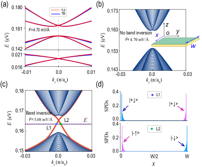
Edge states in an InSb nanolayer with a finite width.—The nontrivial topology can also be manifested by the presence of edge states and the quantum spin Hall effect in a band-inverted InSb nanolayer Hall-bar structure. To demonstrate this, we consider an InSb nanolayer with a finite width as shown in the inset of Fig. 4(b). In principle, the energy spectrum of the system can be obtained by the TB method. However, due to lack of translational symmetry in the planar transverse direction and thus an explosively enlarged unit cell, it requires a significantly large amount of computing resources to obtain the band spectrum. Here, to overcome this difficulty, we employe an effective kp Hamiltonian, which is obtained by fitting to the inverted bands of a corresponding 2D InSb nanolayer obtained by the full TB calculations.
Since only the topologically nontrivial edge states in the band-inverted energy gap will be considered, the effective Hamiltonian can be represented in the six-band basis of . Up to second order in the in-plane wave vector , the Hamiltonian can be written as,
| (5) |
with , , and . Here, , , , are the Pauli matrices in the electron basis and , the angular momentum matrices in the angular momentum hole basis and , () and () are the strengths of the electron (hole) Rashba and Dresselhuas SOCs, denote the strengths of other coupling interactions within the hole basis, correspond to the matrices describing the hybridization of the electron and hole basis states, and denote the hybridization strength Winkler2003 . Note that this effective Hamiltonian is reduced to the Bernevig-Hughes-Zhang (BHZ) Hamiltonian Bernevig2006 , when projected to a lower-dimensional basis of .
Under different electric fields, the coefficients in Eq. (5) can be ascertained by fitting the energy eigenvalues of to the energy band curves obtained by the TB method, as seen in Fig. 4(a). For the specific values of the fitting parameters of the kp Hamiltonian under different electric fields, we refer Ref. SM, . Concretely, for an InSb nanolayer Hall bar with a finite width, the energy in the transverse direction is quantized and the energy spectrum appears in the form of one-dimensional subbands. Figures 4(b) and 4(c) show the subband structures obtained using the effective Hamiltonian for an InSb nanolayer with a finite width under applied electric fields without and with induced band inversion, respectively. It is evidently seen in Fig. 4(c) that being different from the case without the band inversion, there exist four gapless energy bands inside the band-inverted energy gap. These four gapless energy bands exhibit linear energy dispersion relations (the Dirac bands) near the crossing point (the Dirac point). Figure 4(d) shows the probability distributions of the four gapless band states at a fixed energy near the Dirac point. Due to the hybridization between the electron and hole basis states, we can introduce a composite vector operator to calibrate the effective spin direction of the gapless states SM . In the band-inverted nanolayer, it is confirmed that the two states residing at each side of the Hall bar are characterized by different spin orientations (which are closely parallel and antiparallel to the -axis) and distinct propagating directions, i.e., by the quantum spin Hall edge states.
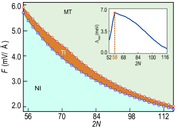
Phase diagram of an InSb nanolayer.—Figure 5 displays the phase diagram of the InSb nanolayer with changing nanolayer thickness and electric field. It is shown that the strength of the critical field at which the phase transition occurs decreases with increasing layer thickness. It is also clearly seen that there presents a stripe of the topologically nontrivial phase (dark colored TI region) in the phase diagram, separating the regions of the trivial insulator phase (NI region) and metallic phase (MT region). The inset of Fig. 5 shows the maximum value of the topological gap , which could be found in the topological phase, as a function of layer thickness. It is found that increases with increasing layer thickness for a thin InSb nanolayer and, after reaching a value of meV, turns to decrease with increasing layer thickness. In principle, the size of the topological gap is largely related to the hybridization of the electron and hole states located close to the two opposite surfaces after the band inversion. Thus, would continuously increase with shrinking layer thickness. However, due to the presence of the -valley conduction band states with a heavy effective mass and the fact that the upper inverted bands near the point has been largely pushed up by quantum confinement, the size of the topological gap has been compromised by the conduction band states near the -valley [cf. Figs. 3(d) and 3(e)]. Similarly, for an InSb nanolayer with a sufficiently small layer thickness, the stripe width of the topological insulator phase is not increased with decreasing layer thickness as one would expect, but instead it is decreased with decreasing layer thickness due to the presence of the low-energy, heavy -valley electron states.
Discussion and conclusion.—In this work, we have shown that the topologically nontrivial phase can be established in a conventional, narrow bandgap semiconductor nanolayer through application of a perpendicular electric field. The topological phase transition occurs in such a nanolayer when the applied electric field goes beyond a critical strength at which the conduction and valence bands of the nanolayer are inverted. In order to obtain a substantially large inverted topological bandgap, it is preferable to explore a semiconductor nanolayer with a small thickness, as to amplify the degree of the electron-hole hybridization. However, in this case, a combined effect of strong quantum confinement and requirement for applying a large field may result in an unfavorable situation, with a conduction band valley lying below the inverted upper-band minimum, and thus prevent from achieving a desired large topological bandgap. Thus, there is a trade-off between the size of the topological bandgap and the size of the topological phase region (cf. the phase diagram in Fig. 5). Overall, our finding should promote the exploiting of the topological phase transition in conventional semiconductor nanolayers for novel physics studies and for topological quantum computing technology developments. It is also possible to extend the expedient proposal to other layered materials with a suitable-size bandgap.
Acknowledgements.
Acknowledgments.—We thank P. Kotetes, D. E. Liu, Q. F. Sun and J. H. Zhao for useful discussions. This work is supported by the National Natural Science Foundation of China (Grant Nos. 92165208, 11874071, 11974340 and 92265203), the Key-Area Research and Development Program of Guangdong Province (Grant No. 2020B0303060001), and the Chinese Academy of Sciences (Grant Nos. XDB28000000, XDPB22 and QYZDJ-SSWSYS001).References
- (1) X.-L. Qi and S.-C. Zhang, Topological insulators and superconductors, Rev. Mod. Phys. 83, 1057 (2011).
- (2) M. Z. Hasan and C. L. Kane, Colloquium: Topological insulators, Rev. Mod. Phys. 82, 3045 (2010).
- (3) R. M. Lutchyn, E. P. A. M. Bakkers, L. P. Kouwenhoven, P. Krogstrup, C. M. Marcus, and Y. Oreg, Majorana zero modes in superconductor-semiconductor heterostructures, Nat. Rev. Mater. 3, 52-68 (2018).
- (4) S. M. Frolov, M. J. Manfra, and J. D. Sau, Topological superconductivity in hybrid devices, Nat. Phys. 16, 718-724 (2020).
- (5) R. M. Lutchyn, J. D. Sau, and S. Das Sarma, Majorana Fermions and a topological phase transition in semiconductor-superconductor heterostructures, Phys. Rev. Lett. 105, 077001 (2010).
- (6) Y. Oreg, G. Refael, and F. von Oppen, Helical liquids and Majorana bound states in quantum wires, Phys. Rev. Lett. 105, 177002 (2010).
- (7) V. Mourik, K. Zuo, S. M. Frolov, S. R. Plissard, E. P. A. M. Bakkers, and L. P. Kouwenhoven, Signatures of Majorana fermions in hybrid superconductor-semiconductor nanowire devices, Science 336, 1003-1007 (2012).
- (8) M. T. Deng, C. L. Yu, G. Y. Huang, M. Larsson, P. Caroff, and H. Q. Xu, Anomalous Zero-bias conductance peak in a Nb-InSb nanowire-Nb hybrid Device, Nano Lett. 12 (12) 6414-6419 (2012).
- (9) M. T. Deng, S. Vaitiekenas, E. B. Hansen, J. Danon, M. Leijnse, K. Flensberg, J. Nygård, P. Krogstrup, and C. M. Marcus, Majorana bound state in a coupled quantum-dot hybrid-nanowire System, Science 354, 1557-1562 (2016).
- (10) M. Aghaee et al. (Microsoft Quantum), InAs-Al hybrid devices passing the topological gap protocol, Phys. Rev. B 107, 245423 (2023).
- (11) J. Alicea, Y. Oreg, G. Refael, F. von Oppen, and M. P. A. Fisher, Non-Abelian statistics and topological quantum information processing in 1D wire networks, Nature Phys. 7, 412-417 (2011).
- (12) S. Das Sarma, M. Freedman, and C. Nayak, Majorana zero modes and topological quantum computation, npj Quantum Information 1, 15001 (2015).
- (13) D. Aasen, M. Hell, R. V. Mishmash, A. Higginbotham, J. Danon, M. Leijnse, T. S. Jespersen, J. A. Folk, C. M. Marcus, K. Flensberg, and J. Alicea, Milestones Toward Majorana-Based Quantum Computing, Phys. Rev. X 6, 031016 (2016).
- (14) R. Aguado and L. P. Kouwenhoven, Majorana qubits for topological quantum computing, Physics Today 73, 6, 44 (2020).
- (15) L. Fu and C. L. Kane, Superconducting proximity effect and majorana fermions at the surface of a topological insulator, Phys. Rev. Lett. 100, 096407 (2008).
- (16) B. van Heck, T. Hyart, C. W. J. Beenakker, Minimal circuit for a flux-controlled Majorana qubit in a quantum spin-Hall insulator, Phys. Scr. T 164, 014007 (2015).
- (17) B. Lian, X.-Q. Sun, A. Vaezi, X.-L. Qi, and S.-C. Zhang, Topological quantum computation based on chiral Majorana fermions, PNAS 115 (43) 10938-10942 (2018).
- (18) F. Schulz, K. Plekhanov, D. Loss, and J. Klinovaja, Majorana bound states in topological insulators with hidden Dirac points, Phys. Rev. Research 2, 033215 (2020).
- (19) Guo-Liang Guo, Han-Bing Leng, Xin Liu, Parity-protected superconducting qubit based on topological insulators, arXiv:2308.12027.
- (20) M. de la Mata, R. Leturcq, S. R. Plissard, C. Rolland, C. Magén, J. Arbiol, P. Caroff, Twin-Induced InSb Nanosails: A Convenient High Mobility Quantum System, Nano Lett. 16, 825-833 (2016).
- (21) D. Pan, D. X. Fan, N. Kang, J. H. Zhi, X. Z. Yu, H. Q. Xu, J. H. Zhao, Free-Standing Two-Dimensional Single-Crystalline InSb Nanosheets, Nano Lett. 16, 834-841 (2016).
- (22) D. Pan, J.-Y. Wang, W. Zhang, L. Zhu, X. Su, F. Fan, Y. Fu, S. Huang, D. Wei, L. Zhang, M. Sui, A. Yartsev, H. Q. Xu, and J. Zhao, Dimension Engineering of High-Quality InAs Nanostructures on a Wafer Scale, Nano Lett. 19, 1632-1642 (2019).
- (23) J. Zhi, N. Kang, F. Su, D. Fan, S. Li, D. Pan, S. P. Zhao, J. Zhao, and H. Q. Xu, Coexistence of induced superconductivity and quantum Hall states in InSb nanosheets, Phys. Rev. B 99, 245302 (2019).
- (24) N. Kang, D. Fan, J. Zhi, D. Pan, S. Li, C. Wang, J. Guo, J. Zhao, and H. Q. Xu, Two-Dimensional Quantum Transport in Free-Standing InSb Nanosheets, Nano Lett. 19, 561-569 (2019).
- (25) Y. Chen, S. Huang, D. Pan, J. Xue, L. Zhang, J. Zhao, and H. Q. Xu, Strong and tunable spin-orbit interaction in a single crystalline InSb nanosheet, npj 2D Mater. Appl. 5, 3 (2021).
- (26) F. Fan, Y. Chen, D. Pan, J. Zhao, and H. Q. Xu, Electrically Tunable spin-orbit interactions in an InAs nanosheet, Nanoscale Advances 4, 2642-2648 (2022).
- (27) L. Zhang, Y. Chen, D. Pan, S. Huang, J. Zhao, and H. Q. Xu, Fabrication and characterization of InSb nanosheet/hBN/graphite heterostructure devices, Nanotechnology 33, 325303 (2022).
- (28) L. Zhang, D. Pan, Y. Chen, J. Zhao, and H. Q. Xu, Quantum oscillations in a hexagonal boron nitride-supported single crystalline InSb nanosheet, Chin. Phys. B 31, 098507 (2022).
- (29) S. Yan, H. Su, D. Pan, W. Li, Z. Lyu, M. Chen, X. Wu, L. Lu, J. Zhao, J.-Y. Wang, and H. Q. Xu, Supercurrent, Multiple Andreev Reflections and Shapiro Steps in InAs Nanosheet Josephson Junctions, Nano Lett. 23, 6497-6503 (2023).
- (30) P. Vogl, H. P. Hjalmarson, and J. D. Dow, A Semi-empirical tight-binding theory of the electronic structure of semiconductors, J. Phys. Chem. Solids 44, 365 (1983).
- (31) M. P. Persson and H. Q. Xu, Electronic structure of [100]-oriented free-standing InAs and InP nanowires with square and rectangular cross sections, Phys. Rev. B 73, 125346 (2006).
- (32) G. Liao, N. Luo, K.-Q. Chen, and H. Q. Xu, Electronic structures of -oriented free-standing InAs and InP nanowires, J. Phys.: Condens. Matter 28, 135303 (2016).
- (33) See the Supplemental Material in which detailed descriptions for and additional results obtained from the calculations of the band structures and topological invariants of an InSb nanolayer under different applied perpendicular electrical fields as well as the calculations of the subband structure and topological edge states of an InSb nanolayer with a finite width are presented.
- (34) X.-B. Xiao, Q. Ye, Z.-F. Liu, Q.-P. Wu, Y. Li, and G.-P. Ai, Electric Field Controlled Indirect-Direct-Indirect Band Gap Transition in Monolayer InSe, Nanoscale Res. Lett. 14, 322 (2019).
- (35) L. Fu and C. L. Kane, Topological insulators with inversion symmetry, Phys. Rev. B 76, 045302 (2007).
- (36) A. A. Soluyanov and D. Vanderbilt, Wannier representation of Z2 topological insulators, Phys. Rev. B 83, 035108 (2011); Computing topological invariants without inversion symmetry, Phys. Rev. B 83, 235401 (2011).
- (37) R. Yu, X. L. Qi, A. Bernevig, Z. Fang and Xi Dai, Equivalent expression of Z2 topological invariant for band insulators using the non-Abelian Berry connection, Phys. Rev. B 84, 075119 (2011).
- (38) G. Klimeck, R. C. Bowen, T. B. Boykin, T. A. Cwik, Tight-binding parameters for transport simulations in compound semiconductors, Superlatt. Microstruct. 27, 519 (2000).
- (39) R. Winkler, Spin-orbit Coupling Effects in Two-dimensional Electron and Hole Systems, (Springer, Berlin, 2003).
- (40) B. A. Bernevig, T. L. Hughes, S.-C. Zhang, Quantum Spin Hall Effect and Topological Phase Transition in HgTe Quantum Wells, Science 314, 1757-1761 (2006).