Understanding the large shift photocurrent of WS2 nanotubes: A comparative analysis with monolayers
Abstract
We study the similarities and differences in the shift photocurrent contribution to the bulk photovoltaic effect between transition-metal dichalcogenide monolayers and nanotubes. Our analysis is based on density functional theory in combination with the Wannier interpolation technique for the calculation of the shift photoconductivity tensor. Our results show that for nanotube radii of practical interest Å, the shift photoconductivity of a single-wall nanotube is well described by that of the monolayer. Additionally, we quantify the shift photocurrent generated under realistic experimental conditions like device geometry and absorption capabilities. We show that a typical nanotube can generate a photocurrent of around 10 nA, while the monolayer only attains a maximum of 1 nA. This enhancement is mainly due to the larger conducting cross section of a nanotube in comparison to a monolayer. Finally, we discuss our results in the context of recent experimental measurements on WS2 monolayer and nanotubes [Zhang et al., Nature 570, 349 (2019)].
I Introduction
The bulk photovoltaic effect (BPVE) offers a promising alternative to traditional solar cells thanks to its ability to generate a d.c. current upon light absorption in homogeneous materials. This effect is described as a second-order optical process; hence, it can only take place in crystal structures that break inversion symmetry Sturman and Fridkin (2021); Fridkin (2001). The photovoltage attained in the BPVE is not limited by the band gap of the material, giving rise to large measured values Spanier et al. (2016); Osterhoudt et al. (2019).
In the last years, the study of the BPVE, and in particular the shift-current contribution, has witnessed a reinvigorated interest Young et al. (2012); Zhang et al. (2019a); Ma et al. (2019); Yang et al. (2018). While traditionally this effect has been mostly studied in bulk ferroelectrics such as BaTiO3 Koch et al. (1975); Young and Rappe (2012), recent theoretical works have emphasized that the shift current undergoes a significant enhancement in two-dimensional (2D) systems such as single-layer monochalcogenides Cook et al. (2017); Rangel et al. (2017). Current efforts include searching for suitable crystal structures with 2D-like properties, in the hope that they may yield an efficient harvesting of light Kwak (2019); Bernardi et al. (2013).
In this context, nanotubes, which consist of a stack of rolled monolayers, offer an ideal bridge between a purely 2D system and a bulk crystal structure. Early theoretical work by Král and co-workers Král et al. (2000) showed the possibility of generating a net shift current in acentric and polar BN nanotubes. In addition to the quasiparticle contribution, the role of excitons (collective excitations composed by electron-hole pairs) in enhancing the nonlinear light-absorption process has also been addressed Konabe (2021); Huang et al. (2023). Low-dimensional transition metal-dichalcogenides (TMDs) also show very good potential as solar-cell devices due to their capacity to absorb a substantial amount of light in the visible range Bernardi et al. (2013), and they are also ideal platforms to study van der Walls interactions and excitonic effects, among other phenomena McCreary et al. (2018). Interestingly, a recent experiment on WS2 TMD nanotubes reported a short-circuit current of around 10 nA Zhang et al. (2019b), yielding one of the largest figure-of-merit reported to date for nonlinear processes. This remarkable value may find its origin on the shift-current contribution Kim et al. (2022), which is allowed by the lack of inversion symmetry of these TMD polytypes.
In this work we perform a systematic study of the shift current in WS2 monolayer and nanotube structures in order to discern the similarities and differences between the two. Our analysis is based on ab-initio density functional theory (DFT) in combination with Wannier-interpolation techniques for an efficient and accurate calculation of the shift photoconductivity tensor Ibañez-Azpiroz et al. (2018). We find that the optical properties of a single-wall nanotube are well described by those of a monolayer for nanotube radii larger than Å, which is generally the range of practical interest. While the shift photoconductivity of the nanotube is somewhat modified by interactions between walls for typical interwall distances, we do not find a substantial and systematic enhancement. Despite possessing a similar shift photoconductivity, we show that a WS2 nanotube can generate a photocurrent of around 10 nA, while the monolayer attains a maximum photocurrent of order 1 nA. Finally, we compute the angular current distribution of both nanotube and monolayer and compare it with the one recently measured in experiment Zhang et al. (2019b).
The paper is organized as follows. In Section II we discuss technical details regarding the approach to describe the monolayer and nanotube structures and the calculation of optical responses using Wannier interpolation. In Section III we show the bulk of our results; after a brief comment on symmetry considerations (Sec. III.1), we analyze the calculated optical photoconductivies of monolayer and nanotube structures (Sec. III.2) and the generated d.c. photocurrent (Sec. III.3). Finally, in Section IV, we provide the main conclusions, and supplementary calculations are included in the Appendix.
II Methods
We have performed first-principles calculations using DFT as implemented in the siesta code packageSoler et al. (2002). We have used norm-conserving pseudopotentials Pickett (1989); Hamann et al. (1979) and we have treated exchange-correlation effects by means of the local density approximation Ceperley and Alder (1980); Perdew and Zunger (1981). We have used a basis set centered at the transition metal (M) and chalcogen (X) atoms of the double-zeta type with polarization orbitals, and we have tested that the results are virtually unchanged using triple-zeta plus polarization orbitals.
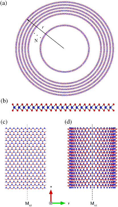
We have considered the trigonal 2H-phase crystal structure Schutte et al. (1987) for modelling TMD monolayers of stoichiometry MX2. Then, by choosing a three-atom fundamental unit domain (one M sandwiched between two X), we have constructed a single-wall nanotube by rolling up the 2D monolayer along the chiral vector defined as , where and are lattice unit vectors of the monolayer and the chiral (integer) indexes determine the chirality of the nanotube. In this work we have focused on the so-called zigzag nanotubes of the type [see 1(d)]. For large , the nanotube radius is proportional to . In our calculations, we have considered the range Å, and we have incorporated a vacuum region of more than 15 Å in every non-periodic direction of the computational slab in order to avoid spurious interactions among the periodic images. Accordingly, we have sampled the Brillouin zone using a -centered k-mesh of 15 15 1 for the monolayer, 10 1 1 for the single-wall nanotube, and 5 1 1 for the double-wall nanotube with mesh cutoff energy of 100 Ry used in all the calculations.
In a postprocessing step, we have calculated maximally localized Wannier functions (MLWFs) Souza et al. (2001); Marzari and Vanderbilt (1997) from a set of Bloch states, using the Wannier90 code package Pizzi et al. (2019). For the monolayer we have constructed 11 MLWFs comprising 7 high-energy valence bands and 4 low-energy conduction bands using and orbitals centered on M and X ions respectively. For the nanotube we have constructed the MLWFs by choosing the localized sets of valence and conduction bands around the Fermi level that comprise the and orbitals centered on all the M and X ions in the slab, which depends on the chiral index .
Finally, we have computed the linear ()
and shift-current () photoconductivities
using the
Wannier-interpolation technique implemented in the postw90
module Pizzi et al. (2019).
We have computed the dipole matrix element
and its covariant derivative entering the expression for the
transition matrix elements Sipe and Shkrebtii (2000)
following the approach
of Refs. Wang et al., 2006
and Ibañez-Azpiroz et al., 2018, respectively.
We employed an interpolation k-mesh and energy smearing width of 10000 10000 1 and 0.02 eV for the monolayer, respectively, and 1000 1 1 and 0.03 eV for the nanotubes, respectively.
III Results
III.1 Symmetry considerations
2D TMD monolayers MX2 are formed by a trigonal prismatic network of M transition metal atoms sandwiched by two inequivalent X chalcogen atoms, as illustrated in Fig.1(b) (side view) and Fig.1(c) (top view). The system breaks inversion symmetry but is symmetric under with a mirror-symmetry plane Mxz denoted in Fig.1(c). The point group of the system is D3h, and the symmetry-allowed components of the shift photoconductivity tensor are (only one independent component).
Regarding the nanotube structure, in this work we will report results on the so-called zigzag configuration, as we have checked that other configurations such as armchair and chiral ones yield similar or slightly smaller optical absorption (this is in line with Ref. Kim et al., 2022). A zigzag nanotube belongs to the isogonal point group C2nv Damnjanović et al. (2017) ( denotes a positive integer number), which contains rotations around the tube axis X and vertical mirror planes such as the one illustrated in Fig. 1(d). The symmetry-allowed tensor components of the shift current are and (two independent components). In practice, this implies that the photocurrent flows only along the direction of the tube axis, irrespective of the light polarization.
III.2 Linear and shift current photoconductivity
III.2.1 Monolayer and single-wall nanotube
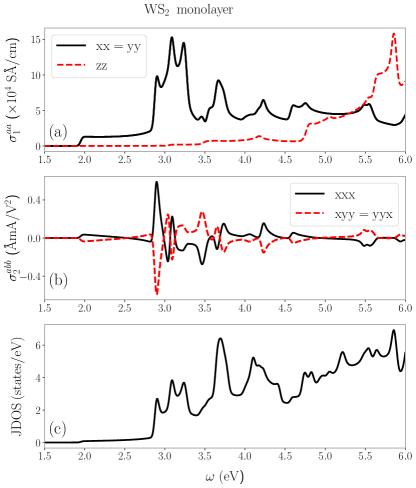
We begin our analysis by studying the linear and shift photoconductivity of WS2 in various forms. Let us start by describing the calculated results for the monolayer, shown in Fig. 2(a,b) together with the corresponding joint density of states (JDOS) in Fig. 2(c), which provides a measure of allowed interband optical transitions Ibañez-Azpiroz et al. (2018); Hu et al. (2019). As expected, the peaks in the various linear and shift photoconductivity spectra coincide with the peaks in the JDOS. Focusing on the shift current, the maximum value takes place at eV, where it reaches ÅmA/V2. As prescribed in Ref. Cook et al., 2017, dividing this figure by the monolayer thickness Å one can obtain an estimated bulk value of about 180 A/V2. This value is significantly larger than the the shift photoconductivity of prototypical ferroelectrics and perovskitesYoung et al. (2012); Zheng et al. (2015); Brehm et al. (2014), and is in line with values reported in other 2D monolayers such as GeS Rangel et al. (2017).
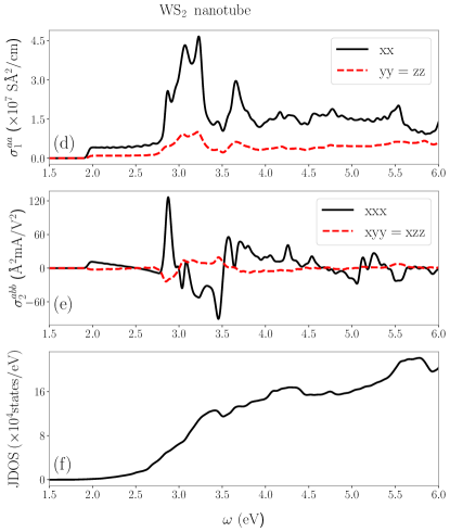
We turn now to analyze the optical properties of a single-wall nanotube of radius Å. The calculated band gap 1.9 eV is very close to that of the monolayer value (see electronic band structures in Appendix), in line with previously reported values Staiger et al. (2012); Zibouche et al. (2012). For both the linear [Fig. 2(d)] and shift current [Fig. 2(e)] spectra, the dominant photoconductivity component corresponds to the tube axis and , respectively. In both cases, the shapes are very similar to the associated components calculated for the monolayer, and the maximum shift current reaches 120 Å2mA/V2. Note, however, that due to the difference in units between Fig. 2(b) and Fig. 2(e), a direct quantitative comparison between monolayer and nanotube shift photoconductivity is not straightforward.
In order to overcome this subtlety, we have opted for considering a quantity known as the shift distance. This magnitude quantifies the real-space distance travelled by electronic carriers upon photoexcitation as a consequence of the shift-current mechanismNastos and Sipe (2006). It is defined as
| (1) |
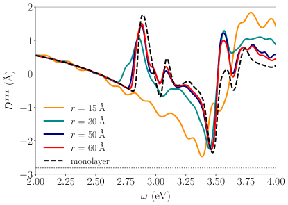
where is the complex dielectric function within the independent-particle approximation, with the vacuum permittivity and as electron charge. Since Eq. 1 involves a ratio between the quadratic and linear absorption coefficients, the shift distance has always length units, allowing a direct comparison of monolayer and nanotube results. In Fig. 3 we show the calculated results of the main component for the monolayer as well as for single-wall nanotubes for radii ranging from 15 to 60 Å. While the peak structure closely follows that of optical properties in all cases, the shape is significantly altered, showing maxima at eV. Overall, the calculated shift distance is of the order of the average bond length between SS and WS atoms in the monolayer configuration, indicated in the figure. This magnitude is in line with what has been previously reported in bulk materials Nastos and Sipe (2006); Ibañez-Azpiroz et al. (2020).
We end this section by inspecting the dependence of the shift distance on the nanotube radius. For a nanotube with Å, we find no peak at and the shape of deviates significantly from the monolayer result. However, as is increased the nanotube shift distance tends to match the shape as well as magnitude of the monolayer result; for Å, only slight deviations are visible. This is an important result, as it shows that nanotubes with radius larger than 60 Å fall within the monolayer limit. Given that in reality, all walls of synthesized nanotubes have 60 ÅZak et al. (2010); Qin et al. (2017), their optical properties can be conveniently described by those of the monolayer, provided interwall interactions are not too large. The latter are analyzed in the following section.
III.2.2 Double-wall nanotube
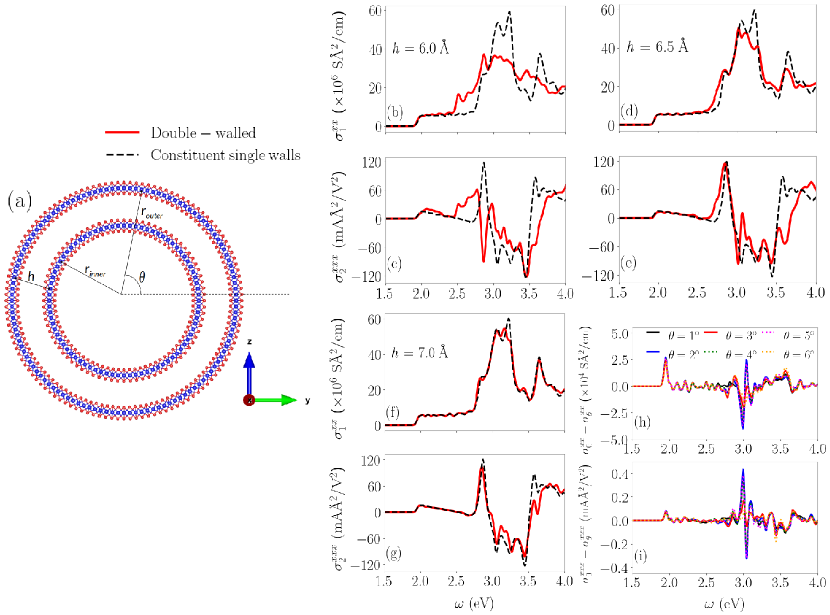
Here we report on the linear and shift
photoconductivity of a double-wall
WS2 nanotube; see Fig. 4(a) for a schematic illustration. For their construction, we stacked two single-wall zigzag nanotubes of different radius on one another.
In our calculations, we have fixed the radius of the inner wall
at Å and varied the radius of the outer wall
in order to sample the photoresponse for varying
interwall distance .
The interwall
distance in the ideal WS2 bilayer
structure is Å,
which increases by in nanotubes Zak et al. (2010); Brüser et al. (2014).
Having this in mind,
in Figs. 4(b)-(e) we show the calculated
and for 6 Å, 6.5 Å and 7 Å.
In addition to the double-wall results, we have also included
results corresponding to the
individual constituent walls, hence
the difference between the two sets can be attributed to the
interwall interaction.
Figs. 4(b)-(c) for Å show that, while the interwall interaction induces visible deviations from the single wall result, it does not alter the order of magnitude of the optical responses. The largest effect on the shift current takes place at 2.9 eV, where peak of the double-wall result flips the sign. However, already for Å [Figs. 4(d)-(e)] the interwall interaction induces only minor differences with respect to the single wall result, and the main spectral features are practically restored. Given that synthesized WS2 nanotubes are likely to have an interwall distance closer to 6.5 Å than 6.0 Å, our calculations indicate that the interwall interaction does not affect the photoresponse properties to the extent that it could explain the enhancement reported in the experiment of Ref. Zhang et al., 2019b. We have verified that this holds for different rotation angles of one wall with respect to the other [see Fig. 4(h)-(i)] as well as for other values of the inner and outer walls (keeping the considered range of interwall distance).
The above results are in apparent contrast to some of the results reported in Ref. Kim et al., 2022, where an acute enhancement of the shift photoconductivity (but not of the linear absorption) was observed in double-wall nanotubes with interwall distance around Å, which was attributed to a wall-to-wall charge shift. We have not found evidence of this enhancement in our calculations, even when using the same radii reported in Ref. Kim et al., 2022. We note that, unlike in the theoretical approach employed in Ref. Kim et al., 2022, we do not resort to a tight-binding model derived from Wannier functions as we keep the whole matrix structure of both the Hamiltonian as well as the position matrix elements Ibañez-Azpiroz et al. (2018). This might explain part of the difference with the results of that work, given that position matrix elements can play an important role in the shift-current generation Ibañez-Azpiroz et al. (2022).
III.3 Total current: monolayer vs nanotube
III.3.1 Estimates of relevant quantities
We turn now to analyze the factors involved in the generation of the total shift current of WS2 monolayer and nanotube. For a material with thickness , the shift current generated under linearly polarized light in a direction normal to the incidence can be written as Fei et al. (2020)
| (2) |
with and the speed of light. There are several quantities entering the above expression, which we now discuss one by one in the context of the experimental setup of Ref. Zhang et al., 2019b.
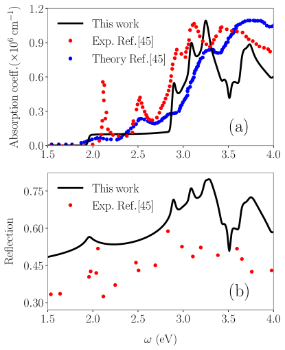
The factor describes the portion of light that is not reflected at the surface between the vacuum and the material. It involves the reflectivity
| (3) |
where the coefficients and are related to the real (R) and imaginary (I) parts of the complex dielectric function as and . In Fig. 5(b) we show the calculated reflectivity factor . It shows that at the band-edge approximately half the incoming light is reflected, whereas, at the peak energy eV approximately 70 of light is reflected; both these values are in rather good agreement with experimental measurements of Ref. Liu et al., 2020, which we have reproduced in the figure. Given that the reflectivity is mainly a surface property, we assume that the same factor applies to the monolayer and the nanotube. This is backed up by a recent experiment on WS2 nanotubes and 2D sheets, which displays very similar levels of reflection intensity for most frequenciesLiu et al. (2019).
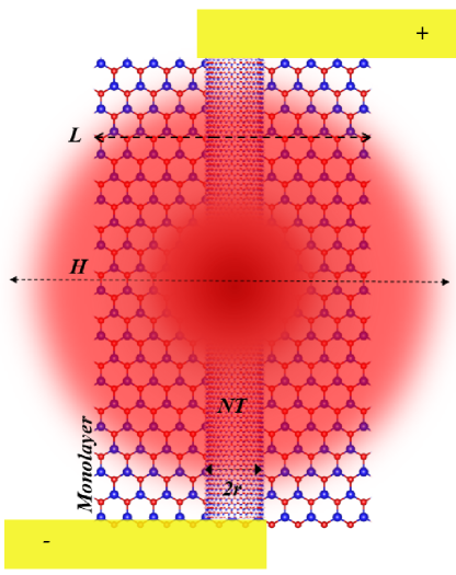
The factor in Eq. 2 accounts for the intensity of the electric field. Ref. Zhang et al., 2019b employed a Gaussian beam, and for a laser of 632.8 nm wavelength, the average electric field strength (or power density) over the spotsize is W/cm2. This number describes appropriately the action of the electric field over the monolayer, given that its dimensions described by m are of the order of the spotsize diameter m Zhang et al. (2019b) (see Fig. 6 for a sketch). In turn, the effective strength of the electric field acting on the nanotube is larger than the average value, given that it is placed in the middle of the laser spotsize where light intensity is highest and its radius nm is small in comparison to (see Fig. 6). Considering the Gaussian profile employed in Ref. Zhang et al., 2019b, we find that the effective strength in the nanotube is approximately larger than the average value, hence, we use W/cm2 for the nanotube.
Finally, we come to analyze the geometric and light-absorption terms in Eq. 2. The symbol denotes the length of the material exposed to light illumination, which is in the case of the monolayer and for the nanotube (see Fig. 6). Plugging the numbers we get that , reflecting the fact that the monolayer is much wider than the nanotube diameter. On the other hand, in Eq. 2 stands for the Glass coefficient Glass et al. (1974); Tan et al. (2016)
| (4) |
with the dielectric constant of the material. The Glass coefficient thus involves the ratio between the shift current and the absorption coefficient Fei et al. (2020)
| (5) |
The inverse of the absorption coefficient describes the light penetration depth into the material. We note that, in the limit of thin materials, , and therefore, the expression of Eq. 2 reduces to , which is independent of and involves the cross section normal to the flow of current.
In Fig. 5(a) we show the calculated absorption coefficient for WS2. The figure shows that ranges between 1 cm-1 at the band-edge and 5 cm-1 at the peak energy eV. These values are in good agreement with previously reported experimental measurements and theoretical estimates of Liu et al. (2020). In practical terms, this means that the light penetration depth ranges between 1000 at the band-edge and 200 at eV. In the case of the monolayer, its thickness is orders of magnitude smaller than the penetration depth. As for the nanotube, it is typically composed of 25 layers and light traverses them twice in most regions. Considering the interwall distance of 6.5 Zak et al. (2010); Brüser et al. (2014), a nanotube is roughly thick; given that , most layers of the nanotube are active in absorbing light. This in turn means that , reflecting the fact that a nanotube is much “thicker” than a monolayer. Combining with the width factor discussed earlier, we conclude that , which represents roughly an order of magnitude enhancement of the nanotube as compared to the monolayer.
III.3.2 Angular dependence and magnitude of the photocurrent
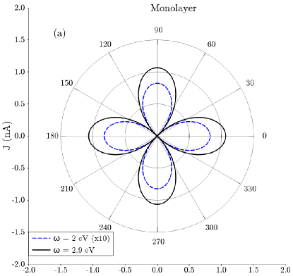
As the last step in our analysis, we study the angular dependence of the shift photocurrent in the two structures based on the arguments of the preceding sections, and quantitatively compare our results to the experimental measurements of Ref. Zhang et al., 2019b. We assume linearly polarized light in the plane under normal incidence, with its electric field described by
| (6) |
The total current generated along the axis can be then expressed as
| (7) |
where gathers the remaining factors of Eq. 2.
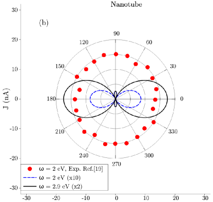
To illustrate our results, in Fig. 7 we have considered two photon energies; 2 eV, where Ref. Zhang et al., 2019b measured maximum current, and 2.9 eV, where our calculations predict maximum shift photoconductivity (see Fig. 2). Let us begin by discussing the monolayer results of Fig. 7(a). Our calculations predict a photocurrent smaller than 0.1 nA for photon energy 2 eV, while at 2.9 eV it is maximum and of the order of nA. To put this into context, BaTiO3 reaches a maximum shift current of 610-3 nA Koch et al. (1975); Young and Rappe (2012). As for the measurements performed in monolayer WS2, Ref. Zhang et al., 2019b did not report a photocurrent larger than 0.1 nA. This suggests that either our calculations overestimate the peak shift-current value by at least an order of magnitude, or some other effect counteracts its contribution. Such effect could be the so-called ballistic current Belinicher et al. (1982); Fridkin (2001), and extrinsic kinetic contribution to the BPVE that can be as large or even larger than the shift current Sturman (2020). In any case, except for the peak magnitude our results on the monolayer are not inconsistent with the experimental findings of Ref. Zhang et al., 2019b, given that in most spectral regions our calculations predict a shift current smaller than 0.1 nA.
We come next to the nanotube results shown in Fig. 7(b); in our calculations, we have disregarded interwall interactions and employed the photoconductivity of a single-wall nanotube with Å, together with Å in Eq. 2 corresponding to a typical nanotube composed of layers Zak et al. (2010); Zhang et al. (2019b). The calculated nanotube photocurrent in Fig. 7(b) ranges between order 1 nA at 2 eV and 10 nA at 2.9 eV, showing an elongated shape around owing to the dominance of over (see Fig. 2). The maximum photocurrent measured in Ref. Zhang et al., 2019b is also of the order of 10 nA, but takes place at 2 eV, coinciding with the energy of the so-called A exciton of WS2. Aside from the mismatch in energy, our calculations show that a zigzag WS2 nanotube with shift photoconductivity equal to the monolayer can account for the order of magnitude measured in Ref. Zhang et al., 2019b. As for the angular dependence, the measured data for the nanotube shows a rounded shape around the origin, but this distribution appears to depend significantly on the precise nanotube that is measured Zhang et al. (2019b).
We note that the nanotubes used in experiment are typically composed of a mixture of internal structures (i.e. zigzag, armchair and chiral) that is in general unknown, and even the radius is not constant throughout the whole nanotube, hence significant deviations from our idealized results are to be expected. Improved theoretical results could be obtained by the modelling of interfaces between different types of structures. Considering many-body interactions in the quadratic photoresponse Luppi et al. (2010); Konabe (2021); Chan et al. (2021); Huang et al. (2023); Garcia-Goiricelaya et al. (2023) could also bring numerical results closer to experiment. In particular, TMDs host the so-called A and B excitons McCreary et al. (2018) that translate into narrow peaks in the spectra (see Fig. 5) which are not captured in our current theoretical description. The few available theoretical works reporting excitonic contributions to the shift current indicate that the effect can be significant Taghizadeh and Pedersen (2018); Konabe (2021); Chan et al. (2021); Huang et al. (2023).
We expect to tackle these aspects in future work.
IV Conclusions
In summary, we have conducted a systematic study of the shift current in WS2 monolayer and nanotube structures. Our DFT calculations have shown that the optical properties of a single wall zigzag nanotube are well described by those of a monolayer for nanotube radius larger than Å. According to our calculations, the single-wall results are only slightly modified when accounting for interactions with other walls of the nanotube for typical interwall distances. Despite possessing a similar shift photoconductivity, we have shown that a WS2 nanotube can generate a photocurrent of around 10 nA, while the monolayer attains a maximum photocurrent of order 1 nA. The main reason behind this difference is the larger conducting cross section of a nanotube in comparison to a monolayer. Our calculations reproduce the order of magnitude of the photocurrent measured in a recent experiment on WS2 nanotubes Zhang et al. (2019b), suggesting that the shift current plays an important role.
V Acknowledgments
We are very grateful to Yijin Zhang for stimulating correspondence. This project has received funding from the European Union’s Horizon 2020 research and innovation programme under the European Research Council (ERC) Grant Agreement No. 946629, and the Department of Education, Universities and Research of the Eusko Jaurlaritza and the University of the Basque Country UPV/EHU (Grant No. IT1527-22).
Appendix: additional calculations
Here we provide additional calculations on electronic structure and optical properties.
.1 Band structure and Wannier interpolation
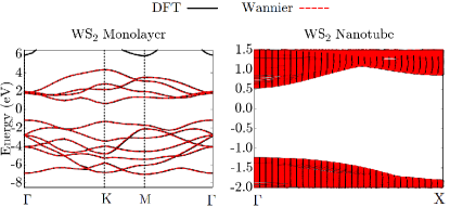
Fig. A1 shows the calculated band structure for WS2 monolayer [Fig. 1(b)] and zigzag nanotube of radius Å [Fig. 1(a)]. We have also included the Wannier-interpolated band structure, which reproduces the DFT one. The figure shows that the direct band gap of the monolayer takes place at high symmetry point K, while in the nanotube it takes place at . The value of the band gap is eV, virtually the same in both structures
.2 Shift current
.2.1 Atomic relaxation
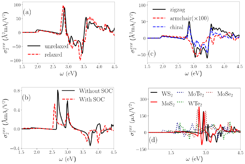
In the calculations in the main text we considered ideal (unrelaxed) atomic positions for the nanotubes. The reason to proceed in this way is twofold. Firstly, we have checked that the relaxation procedure results in changes of the bond lengths below 1 %; this implies that the shift current is only mildly affected as compared to the ideal structure, as exemplified in Fig. A2(a) for a zigzag nanotube of Å. In all calculations, the computed static stress is 0.01 eV Å3. Secondly, working with the ideal atomic structure makes sure that the monolayer and nanotube geometries are as close as possible. This then allows a clear comparison of the optical properties of a monolayer and the corresponding nanotube constructed from it, better highlighting the similarities and differences between them.
.2.2 Spin-orbit coupling
Spin-orbit coupling (SOC) is usually not the main driving effect for the shift current of semiconductors. However, given that tungsten is a heavy element, we have conducted additional calculations on the shift photoconductivity including SOC. We have conducted these calculations using the plane-wave-based QUANTUM ESPRESSO code package Giannozzi et al. (2017), given that the interface to the Wannier90 code package is currently implemented for the case of fully relativistic pseudopotentials. Fig. A2(b) shows the dominant tensor component of the shift photoconductivity of monolayer WS2 calculated with and without SOC. The figure shows that the band-gap energy is reduced by eV as a consequence of SOC, and the main spectral features are somewhat shifted to lower energies roughly by that amount. As expected, the overall order of magnitude of the shift photoconductivity is not altered by SOC. We have verified that this is also the case for calculations of nanotube structures, and that the main results of this work are also not modified by SOC.
.2.3 Nanotube configurations
In addition to the zigzag configuration, an experimentally synthesized TMD nanotube can coexist with two other configurations, namely armchair and chiral . In Fig. A2(c), we present a comparative analysis of the dominant tensor of the shift photoconductivity of three different WS2 nanotube configurations, namely zigzag, armchair and chiral, each with a radius of 30 Å. The figure shows that for the armchair configuration is two orders of magnitude smaller as compared to the zigzag. On the other hand, the shift current of chiral nanotubes follows the same peak trend and same order of magnitude as the zigzag.
.2.4 Different TMDs
Finally, we have extended the calculations to cover the TMD combinations Mo, W and S, Se, Te. Fig. A2(d) shows the calculated (including SOC) of the monolayer structure for all these combinations. As shown by the figure, the overall order of magnitude is the same for all the TMDs, with a maximum shift photoconductivity of 220 A/V2 attained in MoS2.
References
- Sturman and Fridkin (2021) B. I. Sturman and V. M. Fridkin, The Photovoltaic and Photorefractive Effects in Noncentrosymmetric Materials, 1st ed. (Routledge, 2021).
- Fridkin (2001) V. M. Fridkin, Crystallogr. Rep. 46, 654 (2001).
- Spanier et al. (2016) J. E. Spanier, V. M. Fridkin, A. M. Rappe, A. R. Akbashev, A. Polemi, Y. Qi, Z. Gu, S. M. Young, C. J. Hawley, D. Imbrenda, et al., Nature Photonics 10, 611 (2016).
- Osterhoudt et al. (2019) G. B. Osterhoudt, L. K. Diebel, M. J. Gray, X. Yang, J. Stanco, X. Huang, B. Shen, N. Ni, P. J. Moll, Y. Ran, et al., Nature materials 18, 471 (2019).
- Young et al. (2012) S. M. Young, F. Zheng, and A. M. Rappe, Physical review letters 109, 236601 (2012).
- Zhang et al. (2019a) Y. Zhang, T. Holder, H. Ishizuka, F. de Juan, N. Nagaosa, C. Felser, and B. Yan, Nature Communications 10, 3783 (2019a).
- Ma et al. (2019) J. Ma, Q. Gu, Y. Liu, J. Lai, P. Yu, X. Zhuo, Z. Liu, J.-H. Chen, J. Feng, and D. Sun, Nature Materials 18, 476 (2019).
- Yang et al. (2018) M.-M. Yang, D. J. Kim, and M. Alexe, Science 360, 904 (2018).
- Koch et al. (1975) W. Koch, R. Munser, W. Ruppel, and P. Würfel, Solid State Communications 17, 847 (1975).
- Young and Rappe (2012) S. M. Young and A. M. Rappe, Physical Review Letters 109, 116601 (2012).
- Cook et al. (2017) A. M. Cook, B. M. Fregoso, F. De Juan, S. Coh, and J. E. Moore, Nature communications 8, 14176 (2017).
- Rangel et al. (2017) T. Rangel, B. M. Fregoso, B. S. Mendoza, T. Morimoto, J. E. Moore, and J. B. Neaton, Physical Review Letters 119, 067402 (2017).
- Kwak (2019) J. Y. Kwak, Results in Physics 13, 102202 (2019).
- Bernardi et al. (2013) M. Bernardi, M. Palummo, and J. C. Grossman, Nano Letters 13, 3664 (2013).
- Král et al. (2000) P. Král, E. J. Mele, and D. Tománek, Physical Review Letters 85, 1512 (2000).
- Konabe (2021) S. Konabe, Phys. Rev. B 103, 075402 (2021).
- Huang et al. (2023) Y.-S. Huang, Y.-H. Chan, and G.-Y. Guo, Phys. Rev. B 108, 075413 (2023).
- McCreary et al. (2018) K. M. McCreary, A. T. Hanbicki, S. V. Sivaram, and B. T. Jonker, APL Materials 6, 111106 (2018).
- Zhang et al. (2019b) Y. J. Zhang, T. Ideue, M. Onga, F. Qin, R. Suzuki, A. Zak, R. Tenne, J. H. Smet, and Y. Iwasa, Nature 570, 349 (2019b).
- Kim et al. (2022) B. Kim, N. Park, and J. Kim, Nature Communications 13, 1 (2022).
- Ibañez-Azpiroz et al. (2018) J. Ibañez-Azpiroz, S. S. Tsirkin, and I. Souza, Physical Review B 97, 245143 (2018).
- Soler et al. (2002) J. M. Soler, E. Artacho, J. D. Gale, A. García, J. Junquera, P. Ordejón, and D. Sánchez-Portal, Journal of Physics: Condensed Matter 14, 2745 (2002).
- Pickett (1989) W. E. Pickett, Computer Physics Reports 9, 115 (1989).
- Hamann et al. (1979) D. Hamann, M. Schlüter, and C. Chiang, Physical Review Letters 43, 1494 (1979).
- Ceperley and Alder (1980) D. M. Ceperley and B. J. Alder, Physical review letters 45, 566 (1980).
- Perdew and Zunger (1981) J. P. Perdew and A. Zunger, Physical Review B 23, 5048 (1981).
- Schutte et al. (1987) W. Schutte, J. De Boer, and F. Jellinek, Journal of Solid State Chemistry 70, 207 (1987).
- Souza et al. (2001) I. Souza, N. Marzari, and D. Vanderbilt, Physical Review B 65, 035109 (2001).
- Marzari and Vanderbilt (1997) N. Marzari and D. Vanderbilt, Physical review B 56, 12847 (1997).
- Pizzi et al. (2019) G. Pizzi, V. Vitale, R. Arita, S. Bluegel, F. Freimuth, G. Géranton, M. Gibertini, D. Gresch, C. Johnson, T. Koretsune, Ibañez-Azpiroz, H. Lee, J.-M. Lihm, D. Marchand, A. Marrazzo, Y. Mokrousov, J. I. Mustafa, Y. Nohara, Y. Nomura, L. Paulatto, S. Ponce, T. Ponweiser, J. Qiao, F. Thöle, S. S. Tsirkin, M. Wierzbowska, N. Marzari, D. Vanderbilt, I. Souza, A. A. Mostofi, and J. R. Yates, Journal of Physics: Condensed Matter (2019), 10.1088/1361-648X/ab51ff.
- Sipe and Shkrebtii (2000) J. E. Sipe and A. I. Shkrebtii, Physical Review B 61, 5337 (2000).
- Wang et al. (2006) X. Wang, J. R. Yates, I. Souza, and D. Vanderbilt, Physical Review B 74, 195118 (2006).
- Damnjanović et al. (2017) M. Damnjanović, T. Vuković, and I. Milošević, Israel Journal of Chemistry 57, 450 (2017).
- Hu et al. (2019) J.-Q. Hu, X.-H. Shi, S.-Q. Wu, K.-M. Ho, and Z.-Z. Zhu, Nanoscale Research Letters 14, 1 (2019).
- Zheng et al. (2015) F. Zheng, H. Takenaka, F. Wang, N. Z. Koocher, and A. M. Rappe, The journal of physical chemistry letters 6, 31 (2015).
- Brehm et al. (2014) J. A. Brehm, S. M. Young, F. Zheng, and A. M. Rappe, The Journal of chemical physics 141, 204704 (2014).
- Staiger et al. (2012) M. Staiger, P. Rafailov, K. Gartsman, H. Telg, M. Krause, G. Radovsky, A. Zak, and C. Thomsen, Physical Review B 86, 165423 (2012).
- Zibouche et al. (2012) N. Zibouche, A. Kuc, and T. Heine, The European Physical Journal B 85, 1 (2012).
- Nastos and Sipe (2006) F. Nastos and J. Sipe, Physical Review B 74, 035201 (2006).
- Ibañez-Azpiroz et al. (2020) J. Ibañez-Azpiroz, I. Souza, and F. de Juan, Physical Review Research 2, 013263 (2020).
- Zak et al. (2010) A. Zak, L. Sallacan-Ecker, A. Margolin, Y. Feldman, R. Popovitz-Biro, A. Albu-Yaron, M. Genut, and R. Tenne, Fullerenes, Nanotubes, and Carbon Nanostructures 19, 18 (2010).
- Qin et al. (2017) F. Qin, W. Shi, T. Ideue, M. Yoshida, A. Zak, R. Tenne, T. Kikitsu, D. Inoue, D. Hashizume, and Y. Iwasa, Nature communications 8, 14465 (2017).
- Brüser et al. (2014) V. Brüser, R. Popovitz-Biro, A. Albu-Yaron, T. Lorenz, G. Seifert, R. Tenne, and A. Zak, Inorganics 2, 177 (2014).
- Ibañez-Azpiroz et al. (2022) J. Ibañez-Azpiroz, F. de Juan, and I. Souza, SciPost Physics 12, 070 (2022).
- Liu et al. (2020) H.-L. Liu, T. Yang, J.-H. Chen, H.-W. Chen, H. Guo, R. Saito, M.-Y. Li, and L.-J. Li, Scientific Reports 10, 15282 (2020).
- Fei et al. (2020) R. Fei, L. Z. Tan, and A. M. Rappe, Phys. Rev. B 101, 045104 (2020).
- Liu et al. (2019) Z. Liu, A. W. A. Murphy, C. Kuppe, D. C. Hooper, V. K. Valev, and A. Ilie, ACS nano 13, 3896 (2019).
- Glass et al. (1974) A. Glass, D. Von der Linde, and T. Negran, Applied Physics Letters 25, 233 (1974).
- Tan et al. (2016) L. Z. Tan, F. Zheng, S. M. Young, F. Wang, S. Liu, and A. M. Rappe, Npj Computational Materials 2, 1 (2016).
- Belinicher et al. (1982) V. Belinicher, E. Ivchenko, and B. Sturman, Zh. Eksp. Teor. Fiz 83, 649 (1982).
- Sturman (2020) B. I. Sturman, Physics-Uspekhi 63, 407 (2020).
- Luppi et al. (2010) E. Luppi, H. Hübener, and V. Véniard, Phys. Rev. B 82, 235201 (2010).
- Chan et al. (2021) Y.-H. Chan, D. Y. Qiu, F. H. da Jornada, and S. G. Louie, Proceedings of the National Academy of Sciences 118, e1906938118 (2021).
- Garcia-Goiricelaya et al. (2023) P. Garcia-Goiricelaya, J. Krishna, and J. Ibañez-Azpiroz, Phys. Rev. B 107, 205101 (2023).
- Taghizadeh and Pedersen (2018) A. Taghizadeh and T. G. Pedersen, Phys. Rev. B 97, 205432 (2018).
- Giannozzi et al. (2017) P. Giannozzi, O. Andreussi, T. Brumme, O. Bunau, M. B. Nardelli, M. Calandra, R. Car, C. Cavazzoni, D. Ceresoli, M. Cococcioni, et al., Journal of physics: Condensed matter 29, 465901 (2017).