Photo-induced electronic and spin topological phase transitions in monolayer bismuth
Abstract
Ultrathin bismuth exhibits rich physics including strong spin-orbit coupling, ferroelectricity, nontrivial topology, and light-induced structural dynamics. We use ab initio calculations to show that light can induce structural transitions to four transient phases in bismuth monolayers. These light-induced phases exhibit nontrivial topological character, which we illustrate using the recently introduced concept of spin bands and spin-resolved Wilson loops. Specifically, we find that the topology changes via the closing of the electron and spin band gaps during photo-induced structural phase transitions, leading to distinct edge states. Our study provides strategies to tailor electronic and spin topology via ultrafast control of photo-excited carriers and associated structural dynamics.
Bismuth exhibits a rich spectrum of topological phases in all its forms, from monolayer/bilayer to thin film and to bulk Murakami (2006, 2007); Fu et al. (2007); Murakami (2011); Wada et al. (2011); Ning et al. (2014); Drozdov et al. (2014); Lu et al. (2015); Ito et al. (2016); Schindler et al. (2018); Nayak et al. (2019); Hsu et al. (2019); König et al. (2021); Bai et al. (2022). Strong spin-orbit coupling (SOC) motivated early studies of the surface/edge states of 3D bismuth in the context of spin splitting Koroteev et al. (2004); Pascual et al. (2004); Sugawara et al. (2006); Hirahara et al. (2006, 2007); Takayama et al. (2011); Xiao et al. (2012); Takayama et al. (2015). With the advent of topological materials, bismuth was one of the first proposed quantum spin Hall (QSH) insulators in 2D Murakami (2006, 2007) and topological insulators in 3D Fu et al. (2007), both of which have been confirmed experimentally Ning et al. (2014); Drozdov et al. (2014); Lu et al. (2015); Ito et al. (2016). More recently, it has been experimentally shown that bismuth exhibits exotic properties such as topological crystalline insulator states and higher-order topology Schindler et al. (2018); Nayak et al. (2019); Hsu et al. (2019).
In its ultrathin form, bismuth exhibits multiple structural phases, predicted theoretically Singh et al. (2019) and characterized experimentally Nagao et al. (2004). It has been predicted that a puckered monolayer phase exhibits elemental ferroelectricity with switchable in-plane polarization, and this phase can be understood with respect to a paraelectric phase in which there is no puckering Xiao et al. (2018). Recently, such ferroelectric switching has been confirmed experimentally using an in-plane electric field produced by scanning probe microscopy Gou et al. (2023), holding promise for various applications in memory Hong et al. (2023) and energy harvesting Qian et al. (2023) devices. Additionally, several experimental and theoretical works have proposed distinct topological properties for both phases, including Dirac Kowalczyk et al. (2020) and Weyl states Lu et al. (2023) for the ferroelectric phase, 2D topological insulator states Lu et al. (2015) for the paraelectric phase, and generalized QSH states for both phases Bai et al. (2022); Wang et al. (2022). Overall, monolayer bismuth promises to be a fruitful platform to study the interplay between structural, topological, and ferroelectric/paraelectric phases, especially how the topological phase evolves as the structural phase transition takes place.
Among the external stimuli typically used to tune structural phases of bismuth, light can be a relatively simple and economical option, as the structural properties of bismuth are sensitive to photoexcitation energy and fluence, and even small changes in electronic occupation significantly affect its potential energy surface Faure et al. (2013). Indeed, bulk bismuth has served as a reference material for studying photo-excited carrier dynamics and structural dynamics for decades Hase et al. (2002); Murray et al. (2005, 2007); Fritz et al. (2007); Johnson et al. (2009); Timrov et al. (2012); Papalazarou et al. (2012); Faure et al. (2013); Johnson et al. (2013); Perfetti et al. (2015); Murray and Fahy (2015); O’Mahony et al. (2019). In this context, we ask whether monolayer bismuth may be a good candidate for realizing photo-switchable structural and topological properties through phase transitions tuned by photoexcitation energy and fluence. To this end, it would be insightful to investigate whether light can induce phase transitions between the topologically distinct ferroelectric and paraelectric phases, or lead to other hidden phases that cannot be accessed in the dark.
In this Letter, we show that light can be used to control both structural and topological properties of ferroelectric and paraelectric bismuth monolayers. Varying the photo-excited carrier density and electronic temperature, four previously unreported transient inversion symmetric phases are stabilized. We perform a spin band structure analysis Prodan (2009); Lin et al. (2022); Lange et al. (2023) to characterize the topological properties and find that the two dark phases exhibit different QSH insulating behavior with different spin Chern numbers. Remarkably, photo-induced phase transitions drive the ferroelectric and paraelectric phases into 2D Dirac and nodal-line semimetals respectively, each with distinct topological edge states.
Photoexcitation is simulated using two chemical potentials for thermalized electrons and holes respectively Tangney and Fahy (1999, 2002); Murray et al. (2007); Paillard et al. (2016); Haleoot et al. (2017); Paillard et al. (2017, 2019); Gu et al. (2021); Marini and Calandra (2021a, b, 2022), constraining a fixed number of electrons to the conduction bands and holes to the valence bands Peng et al. (2020a, b, 2022). This setup describes an electron-hole plasma state (where excitons are completely screened) and provides an accurate description of optically excited structural dynamics in semimetallic systems such as bulk bismuth Murray et al. (2005, 2007); Fritz et al. (2007); O’Mahony et al. (2019). Density functional theory (DFT) calculations are performed using the Quantum Espresso package Giannozzi et al. (2009, 2020) and Abinit Gonze and et al. (2016, 2020). A fully-relativistic projector augmented wave pseudopotential Dal Corso (2012) is used with the PBEsol exchange-correlation functional Perdew et al. (2008). Kinetic energy cutoffs of Ry and Ry are chosen for the wavefunction and charge density respectively, with a Monkhorst-Pack -point grid of size . A vacuum spacing of 24 Å is employed in combination with the truncation of the Coulomb interaction in the out-of-plane direction Sohier et al. (2017). To analyze the topological properties, maximally localized Wannier functions Marzari and Vanderbilt (1997); Souza et al. (2001); Marzari et al. (2012) for the orbitals are generated using wannier90 Mostofi et al. (2008, 2014); Pizzi et al. (2020). The edge states are computed using WannierTools Wu et al. (2018).
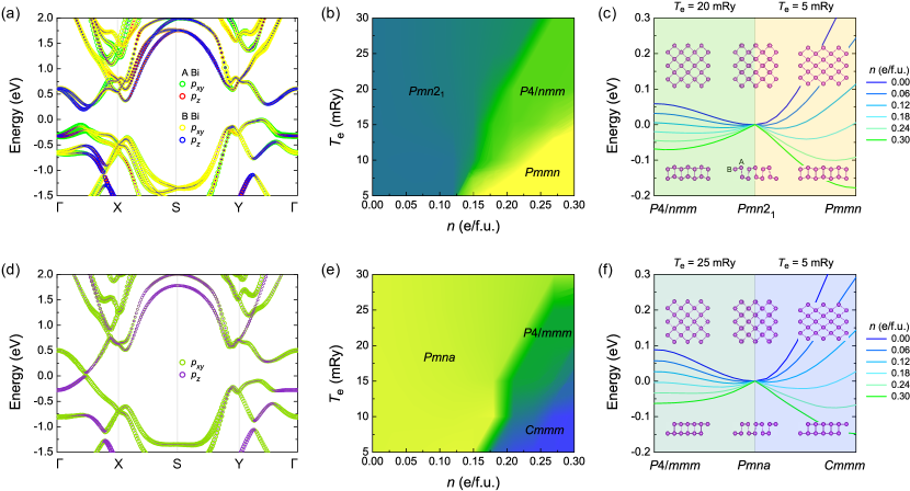
The orbital-projected electronic band structure of the ferroelectric phase is shown in Fig. 1(a). Performing a structural relaxation for different photo-excited carrier densities and electronic temperatures , two paraelectric phases can be obtained, see Fig. 1(b). This is similar to a recent study of ferroelectric perovskites, where the paraelectric phase was predicted to be stabilized by light as carriers effectively screen the polarization Paillard et al. (2017); Peng et al. (2020b). Below mRy (about K), the phase is stabilized at e/f.u. (electron per formula unit). Increasing , the phase becomes energetically favorable.
The crystal structures of the three phases are sketched in the inset of Fig. 1(c). The buckling of the Bi atoms in the same sublayer (labeled A and B) in the phase is also observed in the photo-induced phases. However, the atoms in the sublayers become vertically aligned, restoring inversion symmetry and preventing any polarization. Although both photo-induced phases are paraelectric, they are distinguished by their rectangular () and square () lattices.
To understand whether the photo-induced phases are metastable or transient, we compute the potential energy surfaces of monolayer Bi along the transition paths from ( e/f.u.) to ( e/f.u., mRy) and ( e/f.u., mRy), respectively, for several fixed values of , see Fig. 1(c). In the dark, the phase is unstable. Increasing , the phase becomes stable while the phase becomes unstable, indicating that the phase is transient and can only be accessed by photoexcitation. Similar behavior is observed for the transition from to at mRy.
We also consider the photo-induced transitions starting from the paraelectric phase. Unlike the phase, all four atoms in the phase contribute equally to the electronic states near the Fermi level, see Fig. 1(d). As a result, photoexcitation cannot make the two Bi atoms in the same sublayer asymmetric, i.e. puckering cannot be induced. Two phases are realized upon photoexcitation of the phase: at low and at high , see Fig. 1(e). Neither phase exhibits buckling, see Fig. 1(f), contrary to the phases in Fig. 1(b). The potential energy surfaces from the phase in the dark to the photo-excited phases are shown in Fig. 1(f), indicating that they are also transient and cannot be realized in the dark.
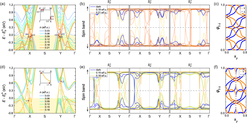
The electronic band structure as a function of carrier density, starting from the phase, is shown in Fig. 2(a). Upon photoexcitation, the gap decreases until the phase transition to at e/f.u., where it closes, indicating that a topological phase transition accompanies the structural transition. For a more refined diagnosis of the topological properties of these phases with fully relativistic SOC included, we consider the spin degree of freedom and examine the spin band structures Prodan (2009); Lin et al. (2022); Lange et al. (2023). We consider the projected spin operator along axis , , where and is the projector onto occupied bands. Importantly, this operator is gauge-invariant provided the electronic band gap does not close Lin et al. (2022); Lange et al. (2023). Diagonalization of leads to spin bands along , which generically do not coincide with the electronic bands and which, for sufficiently strong SOC, can be gapless even when the electronic bands are gapped. Whenever the spin up bands remain separated from the spin down bands however (referred to as the spin gap being open), the spin up/down sectors along are well-defined and their topology can be studied separately, leading to a generalized, -valued QSH effect Prodan (2009, 2010); Yang et al. (2011); Bai et al. (2022), which relies on the presence of a gap in both the energy and the spin spectrum. The spin band structures of the phase are shown in Fig. 2(b). In the dark, the electronic band gap is open as the phase is insulating, and the spin gap is also open along , implying that the spin topology is well defined along these spin directions. By considering the spin- resolved Wilson loop winding Bouhon et al. (2019); Lin et al. (2022); Lange et al. (2023), see Fig. 2(c), we find the spin Chern number for the phase. Thus, the phase in the dark is an exotic doubled QSH insulator with trivial Kane-Mele invariant Kane and Mele (2005a, b); Prodan (2009); Lin et al. (2022), in agreement with Ref. Bai et al. (2022).
The photo-induced phase is a 2D Dirac semimetal because inversion symmetry is restored Young and Kane (2015); Meng et al. (2022); Ding et al. (2022); Yu et al. (2022). The Dirac points D1 and D2 (marked in red) appear along the X–S high-symmetry line and remain nearly fixed for larger , while another Dirac point D3 (marked in white), emerges along –X for e/f.u. The position of the Dirac points in the 2D BZ are shown in the inset of Fig. 2(a). Note that the spin band structure in Fig. 2(b) ceases to be gauge-invariant when the electronic band gap closes. We conclude that the doubled QSH insulator becomes a 2D Dirac semimetal when the structural phase transition takes place.
The band structure as a function of carrier density starting from the paraelectric phase is shown in Fig. 2(d). Under weak or vanishing photoexcitation, the electronic band gap remains open while the spin gap closes for the in-plane spin components and , implying that the spin topology is not well defined along the in-plane directions, see Fig. 2(e). For the out-of plane spin component , the spin gap remains open as long as the electronic gap remains open, suggesting that the effect of SOC is weaker in this direction. For the -directed spin, we find in Fig. 2(f). This suggests that the phase is a QSH insulator as mod , in agreement with Ref. Wang et al. (2022). However, by considering the projected spin band structure within fully relativistic SOC, we can identify this phase as an exotic tripled QSH insulator as long as the gap remains open. The band structures for photo-excited Bi are shown in Fig. 2(d). At e/f.u., the phase transition to takes place and the two bands become degenerate along a nodal line. Thus, the light-induced structural and topological phase transitions occur simultaneously from the QSH insulator with for to the 2D Dirac nodal-line semimetal for .
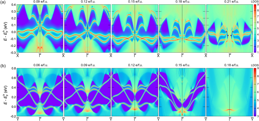
To investigate the boundary signatures Hasan and Kane (2010); Qi and Zhang (2011); Rhim et al. (2018) of the spin topological phases, we plot the (electronic) edge states in Fig. 3. For the phase, we plot the edge states, from 0.09 to 0.21 e/f.u. for = 20 mRy, in Fig. 3(a). Before the phase transition occurs, the doubled QSH insulator displays two pairs of helical edge states which are doubly degenerate at and on the edge (the upper pair partially overlaps with the bulk). In a doubled QSH insulator with conserved , i.e. with quantized eigenvalues, we expect two helical edge states crossing the gap. As is not conserved in our system, the edge states can elastically backscatter pairwise, opening a gap between them Kane and Mele (2005a), as we observe in Fig. 3(a). These edge states are remnants of the bulk topology, but they are not topologically protected, in agreement with the trivial invariant. During the phase transition to the Dirac semimetal, the helical edge states merge into the projections of the bulk Dirac points, connecting the neighboring projected Dirac points.
In Fig. 3(b) we show the edge states of the paraelectric phase from to e/f.u. for mRy. We see a pair of helical edge states crossing the gap, in agreement with the usual phases Kane and Mele (2005a, b). Interestingly, however, we also observe additional edge states, which are weakly gapped out and appear robust up to the phase transition point. Similar to the phase, these are likely remnant edge states, arising due to the fact that the bulk has a high spin Chern number without conservation. After the phase transition, the edge states of the Dirac nodal-line semimetal are hidden in the projections of the bulk states and are only visible around the point at about eV. The split of the edge bands away from the point has been experimentally observed in both Sb and Bi thin films Koroteev et al. (2004); Pascual et al. (2004); Sugawara et al. (2006); Hirahara et al. (2006, 2007); Takayama et al. (2011); Xiao et al. (2012); Takayama et al. (2015), and has been attributed to the strong SOC Hofmann (2006); Bihlmayer et al. (2007).
In summary, we show that light can simultaneously induce transient structural and topological phases in monolayer bismuth, allowing efficient switching between different topologies. By tailoring the photo-excited carrier density and electronic temperature, we find that four hidden crystal structures can be accessed, and in doing so the electronic and spin topological properties may be manipulated, which can be directly measured by existing experimental techniques that have been widely used to study photo-excited dynamics of bismuth. Our findings open a promising route towards ultrafast control of structural, electronic topological properties, as well as spin physics in emerging quantum materials.
Acknowledgements.
B.P., R.J.S. and B.M. acknowledge funding from the Winton Programme for the Physics of Sustainability. B.P. also acknowledges support from Magdalene College Cambridge for a Nevile Research Fellowship. G.F.L. acknowledges funding from the Aker Scholarship. D.B. acknowledges support from the US Army Research Office (ARO) MURI project under grant No. W911NF-21-0147 and the National Science Foundation DMREF program under Award No. DMR-1922172. R.J.S. also acknowledges funding from a New Investigator Award from the EPSRC (EP/W00187X/1) and from Trinity College Cambridge. B.M. also acknowledges support from a UKRI Future Leaders Fellowship (MR/V023926/1) and from the Gianna Angelopoulos Programme for Science, Technology, and Innovation. Calculations were performed using resources provided by the Cambridge Tier-2 system, operated by the University of Cambridge Research Computing Service (www.hpc.cam.ac.uk) and funded by EPSRC Tier-2 capital grant EP/P020259/1, as well as with computational support from the U.K. Materials and Molecular Modelling Hub, which is partially funded by EPSRC (EP/P020194), for which access is obtained via the UKCP consortium and funded by EPSRC grant EP/P022561/1.References
- Murakami (2006) S. Murakami, Phys. Rev. Lett. 97, 236805 (2006).
- Murakami (2007) S. Murakami, New J. Phys. 9, 356 (2007).
- Fu et al. (2007) L. Fu, C. L. Kane, and E. J. Mele, Phys. Rev. Lett. 98, 106803 (2007).
- Murakami (2011) S. Murakami, J. Phys.: Conf. Ser. 302, 012019 (2011).
- Wada et al. (2011) M. Wada, S. Murakami, F. Freimuth, and G. Bihlmayer, Phys. Rev. B 83, 121310(R) (2011).
- Ning et al. (2014) W. Ning, F. Kong, C. Xi, D. Graf, H. Du, Y. Han, J. Yang, K. Yang, M. Tian, and Y. Zhang, ACS Nano 8, 7506 (2014).
- Drozdov et al. (2014) I. K. Drozdov, A. Alexandradinata, S. Jeon, S. Nadj-Perge, H. Ji, R. J. Cava, B. Andrei Bernevig, and A. Yazdani, Nat. Phys. 10, 664 (2014).
- Lu et al. (2015) Y. Lu, W. Xu, M. Zeng, G. Yao, L. Shen, M. Yang, Z. Luo, F. Pan, K. Wu, T. Das, P. He, J. Jiang, J. Martin, Y. P. Feng, H. Lin, and X.-s. Wang, Nano Lett. 15, 80 (2015).
- Ito et al. (2016) S. Ito, B. Feng, M. Arita, A. Takayama, R.-Y. Liu, T. Someya, W.-C. Chen, T. Iimori, H. Namatame, M. Taniguchi, C.-M. Cheng, S.-J. Tang, F. Komori, K. Kobayashi, T.-C. Chiang, and I. Matsuda, Phys. Rev. Lett. 117, 236402 (2016).
- Schindler et al. (2018) F. Schindler, Z. Wang, M. G. Vergniory, A. M. Cook, A. Murani, S. Sengupta, A. Y. Kasumov, R. Deblock, S. Jeon, I. Drozdov, H. Bouchiat, S. Guéron, A. Yazdani, B. A. Bernevig, and T. Neupert, Nat. Phys. 14, 918 (2018).
- Nayak et al. (2019) A. K. Nayak, J. Reiner, R. Queiroz, H. Fu, C. Shekhar, B. Yan, C. Felser, N. Avraham, and H. Beidenkopf, Sci. Adv. 5, eaax6996 (2019).
- Hsu et al. (2019) C.-H. Hsu, X. Zhou, T.-R. Chang, Q. Ma, N. Gedik, A. Bansil, S.-Y. Xu, H. Lin, and L. Fu, Proc Natl Acad Sci 116, 13255 (2019).
- König et al. (2021) C. König, J. C. Greer, and S. Fahy, Phys. Rev. B 104, 035127 (2021).
- Bai et al. (2022) Y. Bai, L. Cai, N. Mao, R. Li, Y. Dai, B. Huang, and C. Niu, Phys. Rev. B 105, 195142 (2022).
- Koroteev et al. (2004) Y. M. Koroteev, G. Bihlmayer, J. E. Gayone, E. V. Chulkov, S. Blügel, P. M. Echenique, and P. Hofmann, Phys. Rev. Lett. 93, 046403 (2004).
- Pascual et al. (2004) J. I. Pascual, G. Bihlmayer, Y. M. Koroteev, H.-P. Rust, G. Ceballos, M. Hansmann, K. Horn, E. V. Chulkov, S. Blügel, P. M. Echenique, and P. Hofmann, Phys. Rev. Lett. 93, 196802 (2004).
- Sugawara et al. (2006) K. Sugawara, T. Sato, S. Souma, T. Takahashi, M. Arai, and T. Sasaki, Phys. Rev. Lett. 96, 046411 (2006).
- Hirahara et al. (2006) T. Hirahara, T. Nagao, I. Matsuda, G. Bihlmayer, E. V. Chulkov, Y. M. Koroteev, P. M. Echenique, M. Saito, and S. Hasegawa, Phys. Rev. Lett. 97, 146803 (2006).
- Hirahara et al. (2007) T. Hirahara, K. Miyamoto, I. Matsuda, T. Kadono, A. Kimura, T. Nagao, G. Bihlmayer, E. V. Chulkov, S. Qiao, K. Shimada, H. Namatame, M. Taniguchi, and S. Hasegawa, Phys. Rev. B 76, 153305 (2007).
- Takayama et al. (2011) A. Takayama, T. Sato, S. Souma, and T. Takahashi, Phys. Rev. Lett. 106, 166401 (2011).
- Xiao et al. (2012) S. Xiao, D. Wei, and X. Jin, Phys. Rev. Lett. 109, 166805 (2012).
- Takayama et al. (2015) A. Takayama, T. Sato, S. Souma, T. Oguchi, and T. Takahashi, Phys. Rev. Lett. 114, 066402 (2015).
- Singh et al. (2019) S. Singh, Z. Zanolli, M. Amsler, B. Belhadji, J. O. Sofo, M. J. Verstraete, and A. H. Romero, J. Phys. Chem. Lett. 10, 7324 (2019).
- Nagao et al. (2004) T. Nagao, J. T. Sadowski, M. Saito, S. Yaginuma, Y. Fujikawa, T. Kogure, T. Ohno, Y. Hasegawa, S. Hasegawa, and T. Sakurai, Phys. Rev. Lett. 93, 105501 (2004).
- Xiao et al. (2018) C. Xiao, F. Wang, S. A. Yang, Y. Lu, Y. Feng, and S. Zhang, Adv. Funct. Mater. 28, 1707383 (2018).
- Gou et al. (2023) J. Gou, H. Bai, X. Zhang, Y. L. Huang, S. Duan, A. Ariando, S. A. Yang, L. Chen, Y. Lu, and A. T. S. Wee, Nature 617, 67 (2023).
- Hong et al. (2023) Y. Hong, J. Deng, X. Ding, J. Sun, and J. Z. Liu, J. Phys. Chem. Lett. 14, 3160 (2023).
- Qian et al. (2023) Z. Qian, J. Zhou, H. Wang, and S. Liu, npj Comput. Mater. 9, 67 (2023).
- Kowalczyk et al. (2020) P. J. Kowalczyk, S. A. Brown, T. Maerkl, Q. Lu, C.-K. Chiu, Y. Liu, S. A. Yang, X. Wang, I. Zasada, F. Genuzio, T. O. Menteş, A. Locatelli, T.-C. Chiang, and G. Bian, ACS Nano 14, 1888 (2020).
- Lu et al. (2023) Q. Lu, P. Reddy, H. Jeon, A. R. Mazza, M. Brahlek, W. Wu, S. A. Yang, J. Cook, C. Conner, X. Zhang, et al., arXiv:2303.02971 (2023).
- Wang et al. (2022) B. Wang, X. Zhou, Y.-C. Lin, H. Lin, and A. Bansil, arXiv:2202.04162 (2022).
- Faure et al. (2013) J. Faure, J. Mauchain, E. Papalazarou, M. Marsi, D. Boschetto, I. Timrov, N. Vast, Y. Ohtsubo, B. Arnaud, and L. Perfetti, Phys. Rev. B 88, 075120 (2013).
- Hase et al. (2002) M. Hase, M. Kitajima, S.-I. Nakashima, and K. Mizoguchi, Phys. Rev. Lett. 88, 067401 (2002).
- Murray et al. (2005) E. D. Murray, D. M. Fritz, J. K. Wahlstrand, S. Fahy, and D. A. Reis, Phys. Rev. B 72, 060301(R) (2005).
- Murray et al. (2007) E. D. Murray, S. Fahy, D. Prendergast, T. Ogitsu, D. M. Fritz, and D. A. Reis, Phys. Rev. B 75, 184301 (2007).
- Fritz et al. (2007) D. M. Fritz, D. Reis, B. Adams, R. Akre, J. Arthur, C. Blome, P. Bucksbaum, A. L. Cavalieri, S. Engemann, S. Fahy, et al., Science 315, 633 (2007).
- Johnson et al. (2009) S. L. Johnson, P. Beaud, E. Vorobeva, C. J. Milne, E. D. Murray, S. Fahy, and G. Ingold, Phys. Rev. Lett. 102, 175503 (2009).
- Timrov et al. (2012) I. Timrov, T. Kampfrath, J. Faure, N. Vast, C. R. Ast, C. Frischkorn, M. Wolf, P. Gava, and L. Perfetti, Phys. Rev. B 85, 155139 (2012).
- Papalazarou et al. (2012) E. Papalazarou, J. Faure, J. Mauchain, M. Marsi, A. Taleb-Ibrahimi, I. Reshetnyak, A. van Roekeghem, I. Timrov, N. Vast, B. Arnaud, and L. Perfetti, Phys. Rev. Lett. 108, 256808 (2012).
- Johnson et al. (2013) S. L. Johnson, P. Beaud, E. Möhr-Vorobeva, A. Caviezel, G. Ingold, and C. J. Milne, Phys. Rev. B 87, 054301 (2013).
- Perfetti et al. (2015) L. Perfetti, J. Faure, E. Papalazarou, J. Mauchain, M. Marsi, M. Goerbig, A. Taleb-Ibrahimi, and Y. Ohtsubo, Journal of Electron Spectroscopy and Related Phenomena 201, 60 (2015).
- Murray and Fahy (2015) E. D. Murray and S. Fahy, Phys. Rev. Lett. 114, 055502 (2015).
- O’Mahony et al. (2019) S. M. O’Mahony, F. Murphy-Armando, E. D. Murray, J. D. Querales-Flores, I. Savić, and S. Fahy, Phys. Rev. Lett. 123, 087401 (2019).
- Prodan (2009) E. Prodan, Phys. Rev. B 80, 125327 (2009).
- Lin et al. (2022) K.-S. Lin, G. Palumbo, Z. Guo, J. Blackburn, D. P. Shoemaker, F. Mahmood, Z. Wang, G. A. Fiete, B. J. Wieder, and B. Bradlyn, arXiv:2207.10099 (2022).
- Lange et al. (2023) G. F. Lange, A. Bouhon, and R.-J. Slager, Phys. Rev. Res. 5, 033013 (2023).
- Tangney and Fahy (1999) P. Tangney and S. Fahy, Phys. Rev. Lett. 82, 4340 (1999).
- Tangney and Fahy (2002) P. Tangney and S. Fahy, Phys. Rev. B 65, 054302 (2002).
- Paillard et al. (2016) C. Paillard, B. Xu, B. Dkhil, G. Geneste, and L. Bellaiche, Phys. Rev. Lett. 116, 247401 (2016).
- Haleoot et al. (2017) R. Haleoot, C. Paillard, T. P. Kaloni, M. Mehboudi, B. Xu, L. Bellaiche, and S. Barraza-Lopez, Phys. Rev. Lett. 118, 227401 (2017).
- Paillard et al. (2017) C. Paillard, S. Prosandeev, and L. Bellaiche, Phys. Rev. B 96, 045205 (2017).
- Paillard et al. (2019) C. Paillard, E. Torun, L. Wirtz, J. Íñiguez, and L. Bellaiche, Phys. Rev. Lett. 123, 087601 (2019).
- Gu et al. (2021) F. Gu, E. Murray, and P. Tangney, Phys. Rev. Mater. 5, 034414 (2021).
- Marini and Calandra (2021a) G. Marini and M. Calandra, Phys. Rev. B 104, 144103 (2021a).
- Marini and Calandra (2021b) G. Marini and M. Calandra, Phys. Rev. Lett. 127, 257401 (2021b).
- Marini and Calandra (2022) G. Marini and M. Calandra, Phys. Rev. B 105, L220406 (2022).
- Peng et al. (2020a) B. Peng, H. Zhang, W. Chen, B. Hou, Z.-J. Qiu, H. Shao, H. Zhu, B. Monserrat, D. Fu, H. Weng, and C. M. Soukoulis, npj 2D Mater. Appl. 4, 14 (2020a).
- Peng et al. (2020b) B. Peng, Y. Hu, S. Murakami, T. Zhang, and B. Monserrat, Sci Adv 6, eabd1618 (2020b).
- Peng et al. (2022) B. Peng, D. Bennett, I. Bravić, and B. Monserrat, Phys. Rev. Mater. 6, L082401 (2022).
- Giannozzi et al. (2009) P. Giannozzi, S. Baroni, N. Bonini, M. Calandra, R. Car, C. Cavazzoni, D. Ceresoli, G. L. Chiarotti, M. Cococcioni, I. Dabo, et al., J. Phys.: Condens. Matter 21, 395502 (2009).
- Giannozzi et al. (2020) P. Giannozzi, O. Baseggio, P. Bonfà, D. Brunato, R. Car, I. Carnimeo, C. Cavazzoni, S. de Gironcoli, P. Delugas, F. Ferrari Ruffino, A. Ferretti, N. Marzari, I. Timrov, A. Urru, and S. Baroni, J. Chem. Phys. 152, 154105 (2020).
- Gonze and et al. (2016) X. Gonze and et al., Comput. Phys. Commun. 205, 106 (2016).
- Gonze and et al. (2020) X. Gonze and et al., Comput. Phys. Commun. 248, 107042 (2020).
- Dal Corso (2012) A. Dal Corso, Phys. Rev. B 86, 085135 (2012).
- Perdew et al. (2008) J. P. Perdew, A. Ruzsinszky, G. I. Csonka, O. A. Vydrov, G. E. Scuseria, L. A. Constantin, X. Zhou, and K. Burke, Phys. Rev. Lett. 100, 136406 (2008).
- Sohier et al. (2017) T. Sohier, M. Calandra, and F. Mauri, Phys. Rev. B 96, 075448 (2017).
- Marzari and Vanderbilt (1997) N. Marzari and D. Vanderbilt, Phys. Rev. B 56, 12847 (1997).
- Souza et al. (2001) I. Souza, N. Marzari, and D. Vanderbilt, Phys. Rev. B 65, 035109 (2001).
- Marzari et al. (2012) N. Marzari, A. A. Mostofi, J. R. Yates, I. Souza, and D. Vanderbilt, Rev. Mod. Phys. 84, 1419 (2012).
- Mostofi et al. (2008) A. A. Mostofi, J. R. Yates, Y.-S. Lee, I. Souza, D. Vanderbilt, and N. Marzari, Comput. Phys. Commun. 178, 685 (2008).
- Mostofi et al. (2014) A. A. Mostofi, J. R. Yates, G. Pizzi, Y.-S. Lee, I. Souza, D. Vanderbilt, and N. Marzari, Comput. Phys. Commun. 185, 2309 (2014).
- Pizzi et al. (2020) G. Pizzi, V. Vitale, R. Arita, S. Blügel, F. Freimuth, G. Géranton, M. Gibertini, D. Gresch, C. Johnson, T. Koretsune, et al., J. Phys.: Condens. Matter 32, 165902 (2020).
- Wu et al. (2018) Q. Wu, S. Zhang, H.-F. Song, M. Troyer, and A. A. Soluyanov, Comput. Phys. Commun. 224, 405 (2018).
- Prodan (2010) E. Prodan, New J. Phys. 12, 065003 (2010).
- Yang et al. (2011) Y. Yang, Z. Xu, L. Sheng, B. Wang, D. Y. Xing, and D. N. Sheng, Phys. Rev. Lett. 107, 066602 (2011).
- Bouhon et al. (2019) A. Bouhon, A. M. Black-Schaffer, and R.-J. Slager, Phys. Rev. B 100, 195135 (2019).
- Kane and Mele (2005a) C. L. Kane and E. J. Mele, Phys. Rev. Lett. 95, 226801 (2005a).
- Kane and Mele (2005b) C. L. Kane and E. J. Mele, Phys. Rev. Lett. 95, 146802 (2005b).
- Young and Kane (2015) S. M. Young and C. L. Kane, Phys. Rev. Lett. 115, 126803 (2015).
- Meng et al. (2022) W. Meng, Y. Liu, W.-W. Yu, X. Zhang, and G. Liu, Mater. Today Physics 27, 100774 (2022).
- Ding et al. (2022) X. Ding, Y. Ge, Y. Jia, G. Gou, Z. Zhu, and X. C. Zeng, ACS Nano 16, 21546 (2022).
- Yu et al. (2022) Z.-M. Yu, Z. Zhang, G.-B. Liu, W. Wu, X.-P. Li, R.-W. Zhang, S. A. Yang, and Y. Yao, Sci. Bull. 67, 375 (2022).
- Hasan and Kane (2010) M. Z. Hasan and C. L. Kane, Rev. Mod. Phys. 82, 3045 (2010).
- Qi and Zhang (2011) X.-L. Qi and S.-C. Zhang, Rev. Mod. Phys. 83, 1057 (2011).
- Rhim et al. (2018) J.-W. Rhim, J. H. Bardarson, and R.-J. Slager, Phys. Rev. B 97, 115143 (2018).
- Hofmann (2006) P. Hofmann, Prog. Surf. Sci. 81, 191 (2006).
- Bihlmayer et al. (2007) G. Bihlmayer, S. Blügel, and E. V. Chulkov, Phys. Rev. B 75, 195414 (2007).
- Zhou et al. (2023) S. Zhou, C. Bao, B. Fan, H. Zhou, Q. Gao, H. Zhong, T. Lin, H. Liu, P. Yu, P. Tang, S. Meng, W. Duan, and S. Zhou, Nature 614, 75 (2023).