ODMR short = ODMR, long = optically detected magnetic resonance, tag = abbrev \DeclareAcronymNMR short = NMR, long = nuclear magnetic resonance, tag = abbrev \DeclareAcronymEM short = EM, long = electromagnetic radiation, tag = abbrev \DeclareAcronymGSLAC short = GSLAC, long = ground state level anticrossing, tag = abbrev \DeclareAcronymMRI short = MRI, long = magnetic resonance imaging , tag = abbrev \DeclareAcronymPID short = PID, long = proportional-integral-derivative controller, tag = abbrev \DeclareAcronymFCC short = FCC, long = face-centred cubic, tag = abbrev \DeclareAcronymNV short = NV, long = nitrogen vacancy, tag = abbrev \DeclareAcronym-NV short = NV-, long = nitrogen vacancy, tag = abbrev \DeclareAcronymSG short = SG, long = signal generator, tag = abbrev \DeclareAcronymFG short = FG, long = function generator, tag = abbrev \DeclareAcronymMW short = MW, long = microwave, tag = abbrev \DeclareAcronymLCAO short = LCAO, long = linear combination of atomic orbitals , tag = abbrev \DeclareAcronymMO short = MO, long = molecular orbitals , tag = abbrev \DeclareAcronymISC short = ISC, long = intersystem crossing , tag = abbrev \DeclareAcronymPL short = PL, long = photo-luminescence, tag = abbrev \DeclareAcronymcw short = cw, long = continuous wave, tag = abbrev \DeclareAcronymMandhala short = Mandhala, long = magnetic arrangement for novel discrete halbach layout, tag = abbrev \DeclareAcronymHPHT short = HPHT, long = high-pressure high-temperature, tag = abbrev \DeclareAcronymSQ short = SQ, long = single quantum, tag = abbrev \DeclareAcronymDQ short = DQ, long = double quantum, tag = abbrev \DeclareAcronymfps short = fps, long = frames per second, tag = abbrev \DeclareAcronymmagnet short = magnet, long = Halbach assembly, tag = abbrev \DeclareAcronymPM short = PM, long = cylindrical permanent magnet, tag = abbrev \DeclareAcronymLM short = LM, long = Levenberg-Marquardt, tag = abbrev \DeclareAcronymFWC short = FWC, long = full well capacity, tag = abbrev \DeclareAcronymFWHM short = FWHM, long = full width at half maximum, tag = abbrev \DeclareAcronymWF short = WF, long = wide-field, tag = abbrev \DeclareAcronymCVD short = CVD, long = chemical vapour deposition, tag = abbrev \DeclareAcronymMEG short = MEG, long = magnetoencephalography, tag = abbrev \DeclareAcronymMCG short = MCG, long = magnetocardiography, tag = abbrev \DeclareAcronymSQUID short = SQUID, long = superconducting quantum interference device, tag = abbrev \DeclareAcronymsCMOS short = sCMOS, long = scientific Complementary Metal-Oxide-Semiconductor, tag = abbrev \DeclareAcronymPSN short = PSN, long = photon shot-noise, tag = abbrev \DeclareAcronymOPM short = OPM, long = optically pumped magentometer, tag = abbrev \DeclareAcronymFPGA short = FPGA, long = field progammable gate array, tag = abbrev \DeclareAcronymESLAC short = ESLAC, long = excited-state level anti-crossing, tag = abbrev \DeclareAcronymSTED short = STED, long = stimulated emission depletion, tag = abbrev
Microwave-free wide-field magnetometry using nitrogen-vacancy centers
Abstract
A wide-field magnetometer utilizing nitrogen-vacancy (NV) centers in diamond that does not require microwaves is demonstrated. It is designed for applications where microwaves need to be avoided, such as magnetic imaging of biological or conductive samples. The system exploits a magnetically sensitive feature of NV centers near the \acGSLAC. An applied test field from a wire was mapped over an imaging area of \qty[parse-numbers=false]≈500×470\squared. Analysis of the \acGSLAC lineshape allows to extract vector information of the applied field. The device allows micrometer-scale magnetic imaging at a spatial resolution dominated by the thickness of the NV layer (here ). For a pixel size of the estimated sensitivity is \qty4.8\micro\per. Two modalities for visualizing the magnetic fields, static and temporal, are presented along with a discussion of technical limitations and future extensions of the method.
I Introduction
Negatively charged \acfNV centers in diamond [1] have attracted significant attention as a promising platform for sensing various physical quantities, such as temperature, pressure, magnetic and electric fields, at the nanoscale under various environmental conditions [2, 3, 4]. Magnetometry based on spin-dependent fluorescence of these \acNV centers has demonstrated sensitivities down to \qty[parse-numbers=false]0.6\pico\per for ensembles at room temperature [5, 6, 7]. By employing \acpODMR with \acNV centers, one can probe the magnetic fields generated by a wide range of samples, including biological systems, magnetic materials, current-carrying wires, and \acpFPGA [8, 6, 9, 10, 11]. In \acODMR based magnetometry, a diamond sample is illuminated with laser light (for example, at 532 nm) and is subjected to a microwave field to drive population transfer between the differently bright spin states. When the microwave frequency matches a transition, there is a decrease of fluorescence. Measuring the resonant frequencies for transitions between the and states allows reconstruction of the magnetic field projection onto the NV axis [4, 12, 13].
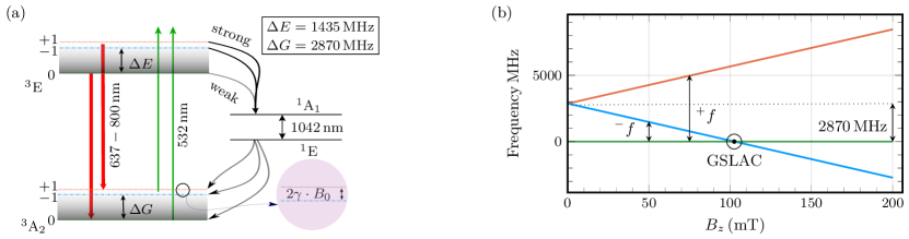
However, there are scenarios where the use of microwaves is undesirable, such as when dealing with conductive materials or sensitive biological samples. To address this, recent developments have focused on microwave-free protocols that exploit energy-level crossings of \acNV centers at different magnetic fields. These protocols include microwave-free magnetometry and vector magnetometry at zero-field, as well as the exploitation of specific features like the \acESLAC feature at 51.2 mT and the \acfGSLAC feature at 102.45 mT [14, 13, 15]. These kind of magnetically sensitive features have been successfully utilized for vector magnetometery, measuring eddy currents in conducting materials and performing \acNMR [16, 17, 18]. In light of these advancements, this report presents a microwave-free wide-field magnetic microscope that leverages the \acGSLAC feature to probe and image samples where microwaves are detrimental.
The \acGSLAC feature originates from the mixing of ground-state levels at 102.45 mT. Due to the Zeeman splitting of the triplet ground state, as illustrated in Fig. 1a, the state becomes degenerate with the state and mixing results in population transfer between these states. Mixing occurs due to hyperfine interaction, cross-relaxation with other defects as well as static and oscillating transversal magnetic fields. The population transfer is observed as a drop in fluorescence intensity. Our study aims to explore the potential of utilizing \acNV centers without the need for microwaves to map magnetic fields. We create static magnetic field maps by analyzing the lineshape of the \acGSLAC resonance pixel by pixel. Furthermore, in another sensing modality, we investigate the sensitivity to dynamic field changes between individual image frames.
To demonstrate the utility of this magnetometer we map the magnetic field distribution of a direct current (DC) field generated by a straight current-carrying wire with a diameter of \qty200 placed on the diamond sample while we image it from underneath. This proof-of-concept experiment explores the application of \acNV centers in a setup without microwaves. The lack of microwaves increases the usability of the device while reducing its technical complexity since no microwave components are needed. The results highlight the viability of diamond-based quantum sensors for a wide range of materials and biological applications.
II Experimental Setup
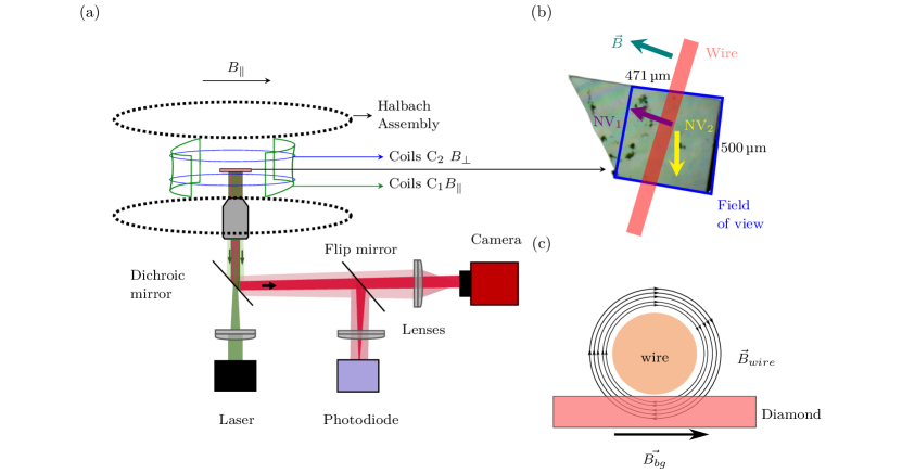
The setup incorporates a \aclmagnet [20, 21], two pairs of coils, a (110) diamond plate and collection optics. The cylindrical \aclmagnet provides a magnetic field orthogonal to its bore with minimal stray field external to the magnet. The diamond is a \acHPHT grown diamond purchased from Element Six with a concentration of \qty3.7 \acNV centers homogeneously distributed. It was cut mechanically from a 13C depleted Ib diamond with a (100) face to a (110) face. The diamond sample dimensions were \qty[parse-numbers=false]1 ×0.5 ×0.05\cubic. It had an initial nitrogen concentration \qty10. It was irradiated with electrons of \qty5\mega, with a dose of \qty2e19\per□ electrons and then annealed at \qty700 for \qty8. The thickness of the NV layer (\qty50) limits the spatial magnetic field resolution [19]. The diamond is shown in Fig. 2b where the field of view is marked in blue, the two NV axes of the diamond orthogonal to the cylinder bore usable for microwave-free magentometry are marked in yellow and violet. We use the orientation marked in violet.
The sample is positioned in the center of the \aclmagnet on a rotatable platform, with its axis of rotation parallel to the \aclmagnet bore perpendicular to the field. This allowed to align the \acNV axis in the (110) plane of the diamond to the \aclmagnet background field produced. The sample is set on a sapphire window with a diameter of \qty10 and a thickness of 0.25 mm. It permits laser-light delivery and collection of light from under the diamond sample while acting as a heat sink.
As shown in Fig. 2 the \aclmagnet is fitted with two sets of Helmholtz coil pairs. Coil pair C1 is oriented in the direction of the background field and coil pair C2 is perpendicular to it and parallel to the cylinder axis. The coils are used to shim the magnetic field of the \aclmagnet and optimize the linewidth and contrast of the \acGSLAC feature. The diamond mount is attached to the C1 coils. It feature a range of \qty[parse-numbers=false]±1.3\milli. The second Helmholtz coil pair (C2) is used to remove residual transverse fields. A third coil pair perpendicular to C1 and C2 would be ideal but was not implemented due to space constraints in the magnet bore.
A \accw 532 nm laser (Laser Quantum, gem532) is used to illuminate the diamond via a microscope objective (Olympus Plan 10X objective). The fluorescent light is gathered using the same objective, reflected off a short-pass dichroic mirror with a cutoff wavelength of 600 nm and passes through a long-pass filter to remove the remaining green reflection of the laser light.
The collected fluorescence is directed to a \acfsCMOS camera (Andor Zyla 5.5) for imaging. Alternatively for diagnostic purposes, the light can be directed to a photodiode (PDA36A2) using a flip mirror.
III Results and Discussions
III.1 Static Imaging
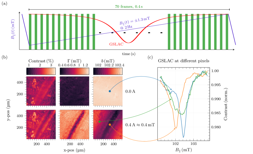
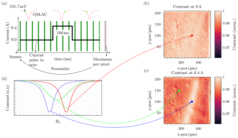
We demonstrate a static magnetic field imaging modality using the \acGSLAC by visualizing the field generated by a wire carrying electric current. The results are presented in Fig. 3b To image , we illuminated the diamond with \accw 532 nm laser light with a Gaussian profile. The laser beam covered an area of \qty[parse-numbers=false]≈0.5×0.47\squared.
The background magnetic field was swept over a range of \qty[parse-numbers=false]102.45±1.3\milli, covering the \acGSLAC feature while images where taken with the camera. This way the individual pixels contain a magnetic field scan over the \acGSLAC feature. The current-carrying wire generates both axial () and transverse components () in the measurement region, thereby leading to alterations in the contrast (C), \acFWHM and the center-field position of the \acGSLAC feature.
To analyze and quantify the observed changes, we fitted the experimental data pixel-by-pixel with a Lorentzian function [22, 23] to extract three fitting parameters: contrast (), \acFWHM (), and center-field ().
To ensure synchronization between the magnetic field ramp and the data acquisition, we employed an external trigger at 185 Hz. This trigger served as a timing reference and triggered the camera to capture 70 frames during a 0.4 s magnetic field ramp.
Additionally, to enhance the signal-to-noise ratio, we repeated the acquisition 20 times and averaged the results.The acquisition procedure, which is similar to that of [24], is illustrated in Fig. 3a.
During data analysis, we extract the \acGSLAC feature from individual pixels within a specific region measuring \qty[parse-numbers=false]≈0.47×0.50□. This region comprises a total of pixels, with each pixel corresponding to an area of on the diamond surface. The extracted data are averaged over a pixels grid. This binning process reduces the optical resolution to approximately which is not limiting the spatial resolution for magnetic fields.
We utilize the \acLM algorithm [25] to fit the binned data on a pixel-by-pixel basis to a Lorentzian function. We extract the fitting parameters for each pixel, which provides information about the magnetic field distribution. The fitting of multiple pixels was done in parallel utilizing a threaded Python script. The resulting data-processing time was \qty136 per image. This is still significantly longer than the data acquisition time and requires further improvement. For example, deploying a parallel fitting routine on a graphics card or \acpFPGA.
The maps presented in Fig. 3b are reconstructed images of a current-carrying wire. As the wire field in the sensor is mostly anti-aligned to the background field (see Fig. 2c), the total magnetic field reduces. The wire field results in a shift and a broadening of the \acGSLAC feature. On examination of the maps, we observe that the width of the feature is smallest at the center of the wire and increases away from it. This is mirrored in the center maps where the change in the total magnetic field is largest under the wire, Fig. 2c and Fig. 3c. This is consistent with a model of the wire magnetic field in the diamond.
In the region under the wire, there is no broadening of \acFWHM caused by transverse fields. As we move away from the center of the wire, the transverse components become dominant, leading to an increase in the observed \acFWHM of the \acGSLAC feature. The center maps in Fig. 3c also demonstrate this effect, with the area nearest to the wire showing a \qty0.5\milli-shift from \qty102.4\milli to \qty101.9\milli when a magnetic field corresponding to a current of 0.4 A is applied. This shift gradually reduces to \qty0.1\milli furthest from the wire.
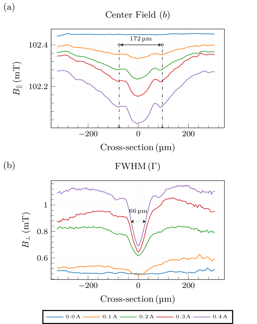
Additionally, we examine an averaged cross-section of the maps in Fig. 4, specifically focusing on the \acFWHM displayed in Fig. 4b. We observe something peculiar: considering the thickness of the \acNV layer in the diamond, which is approximately 50 , the spatial resolution for the magnetic field was expected to be on the order of 50 as well [19]. The wire itself has a diameter of 200 . From observation however, the feature in the image Fig. 4b corresponding to the wire shows a \acFWHM of \qty[parse-numbers=false]≈66 when a field is generated with a wire carrying 0.4 A. Just directly below the wire its field does not feature a transverse component in the NV layer. So just there, no broadening is observed. This effect becomes more pronounced with increasing wire current. It bears some resemblance to super-resolution imaging techniques like \acSTED [26, 27], albeit in the context of magnetic fields. In \acSTED, a laser beam with a donut-shaped cross-section is used to de-excite emitters through stimulated emission for sub-diffraction resolution images.
III.2 Temporal Imaging
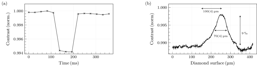
To implement dynamic imaging, we captured a video while pulsing current through the wire. This allows us to observe the magnetic field from the wire in real time. The results are summarized in Fig. 5. The temporal resolution is limited by the camera frame rate, which is set at 39 Hz. The camera can operate at a significantly higher frame rate, however, this reduces the amount of collected photons.
The experimental procedure is illustrated in Fig. 5a. It involves tuning the bias field to the slope of the \acGSLAC feature in at \qty101.7\milli. We then capture 15 frames for \qty380\milli (at a rate of 39 Hz) while turning on a current of 0.4 A through the wire for the central 100 ms. Post acquisition, we normalize the contrast of each individual pixel by its maximum value in the 15 images. This allows a straight-forward comparison of frames taken before and during the current pulse.
In Fig. 5b and Fig. 5c), we present two frames separated by \qty25\milli, respectively. Figure 5b has no current applied through the wire. In figure 5c a current of 0.4 A is applied. We observe changes in contrast in areas away from the wire. This is a result of the transverse components of the magnetic field () generated by the wire. It broadens the \acGSLAC feature. The broadening leads to a decrease in contrast and the corresponding diamond region to appear darker. However, directly under the wire, the magnetic field is aligned with the total field () causing the \acGSLAC resonance to shift to \qty103.2\milli but not to broaden. This is why this region remains bright. We have chosen the values of the bias and the wire fields to maximize the contrast variation between the “on” and “off” frames integrated over the complete image. Furthermore, we chose these parameters to ensure all pixels remain within the \acGSLAC feature and to determine the limit of contrast variations we can visualize.
An analysis of the temporal cross-section of the acquired frames is shown in Fig. 6a. The the applied pulse shape is retrieved. An examination of the cross-section of the wire image is presented in Fig. 6b. We discern maximum contrast variations of up to \qty9 at a distance of \qty100 from the wire center. Beyond this distance, the contrast variations, which is due mostly to the transverse field component of the wire, level off. To further improve the temporal and spatial resolution in this modality, high-frame-rate or lock-in detection-enabled cameras can be employed.
IV Conclusion
We developed a microwave-free diamond magnetic field microscope utilizing NV centers to measure spatially varying magnetic fields over a field of view of approximately \qty[parse-numbers=false]500 ×470. We analyzed the GSLAC feature and can reconstruct longitudinal and transverse components of magnetic fields of samples. We implemented a fitting algorithm to extract the \acGSLAC feature and estimate magnetic fields in an image of pixels post-binning.
Our results demonstrate the potential of microwave-free vector magnetometry with temporal resolution enabling recording of magnetic “movies”. We envision that this approach will have a significant impact across a range of fields, including materials science, biology, and condensed matter physics.
It is important to acknowledge certain limitations in achieving high-resolution magnetic maps using the current methodology. One constraint is that only 1/4 of the NV-center orientations are available for this modality due to the requirement of on-axis alignment with the bias field. This leads to an overall drop in signal. Use of preferentially oriented NV centers could enhance the overall contrast and sensitivity [28].
Another limitation arises from the camera, which imposes constraints in terms of its Full Well Capacity (FWC) and frames per second (fps). The mean per pixel shot-noise limit is estimated to be approximately \qty4.8\micro\per for a pixel size of \qty4, or \qty137.35\micro \raiseto1.5\per for a volume-normalized estimate. This can be compared to the best-reported volume-normalized sensitivities of comparable cameras using microwaves (including lock-in cameras) of approximately \qty31\nano \raiseto1.5\per [29, 30]. Considering these limits, future improvements may involve lock-in-based detection to boost sensitivity and pulse sequences for T1 relaxometry [18].
V Acknowledgment
This work was supported by the German Federal Ministry of Education and Research (BMBF) within the Quantumtechnologien program (DIAQNOS, project no. 13N16455) and by the European Commission’s Horizon Europe Framework Program under the Research and Innovation Action MUQUABIS, project no. 101070546.
References
- [1] J. R. Maze, A. Gali, E. Togan, Y. Chu, A. Trifonov, E. Kaxiras, and M. D. Lukin, “Properties of nitrogen-vacancy centers in diamond: the group theoretic approach,” New Journal of Physics, vol. 13, p. 025025, feb 2011.
- [2] M. Lesik, T. Plisson, L. Toraille, J. Renaud, F. Occelli, M. Schmidt, O. Salord, A. Delobbe, T. Debuisschert, L. Rondin, P. Loubeyre, and J. F. Roch, “Magnetic measurements on micrometer-sized samples under high pressure using designed NV centers,” Science, vol. 366, pp. 1359–1362, 12 2019.
- [3] V. M. Acosta, E. Bauch, M. P. Ledbetter, A. Waxman, L.-S. Bouchard, and D. Budker, “Temperature dependence of the nitrogen-vacancy magnetic resonance in diamond,” Phys. Rev. Lett., vol. 104, no. 7, p. 070801, 2010.
- [4] A. Jarmola, V. Acosta, K. Jensen, S. Chemerisov, and D. Budker, “Temperature-and magnetic-field-dependent longitudinal spin relaxation in nitrogen-vacancy ensembles in diamond,” Physical review letters, vol. 108, no. 19, p. 197601, 2012.
- [5] G. Chatzidrosos, A. Wickenbrock, L. Bougas, N. Leefer, T. Wu, K. Jensen, Y. Dumeige, and D. Budker, “Miniature cavity-enhanced diamond magnetometer,” Phys. Rev. Appl., vol. 8, p. 044019, Oct 2017.
- [6] J. F. Barry, M. J. Turner, J. M. Schloss, D. R. Glenn, Y. Song, M. D. Lukin, H. Park, and R. L. Walsworth, “Optical magnetic detection of single-neuron action potentials using quantum defects in diamond,” Proceedings of the National Academy of Sciences, vol. 113, pp. 14133–14138, nov 2016.
- [7] J. F. Barry, M. H. Steinecker, S. T. Alsid, J. Majumder, L. M. Pham, M. F. O’Keefe, and D. A. Braje, “Sensitive ac and dc magnetometry with nitrogen-vacancy center ensembles in diamond,” 2023.
- [8] M. Karadas, A. M. Wojciechowski, A. Huck, N. O. Dalby, U. L. Andersen, and A. Thielscher, “Feasibility and resolution limits of opto-magnetic imaging of neural network activity in brain slices using color centers in diamond,” Scientific Reports, vol. 8, mar 2018.
- [9] J. L. Webb, L. Troise, N. W. Hansen, C. Olsson, A. M. Wojciechowski, J. Achard, O. Brinza, R. Staacke, M. Kieschnick, J. Meijer, et al., “Detection of biological signals from a live mammalian muscle using an early stage diamond quantum sensor,” Scientific reports, vol. 11, no. 1, pp. 1–11, 2021.
- [10] T. Lenz, G. Chatzidrosos, Z. Wang, L. Bougas, Y. Dumeige, A. Wickenbrock, N. Kerber, J. Zázvorka, F. Kammerbauer, M. Kläui, Z. Kazi, K.-M. C. Fu, K. M. Itoh, H. Watanabe, and D. Budker, “Imaging topological spin structures using light-polarization and magnetic microscopy,” Physical Review Applied, vol. 15, Feb. 2021.
- [11] E. V. Levine, M. J. Turner, P. Kehayias, C. A. Hart, N. Langellier, R. Trubko, D. R. Glenn, R. R. Fu, and R. L. Walsworth, “Principles and techniques of the quantum diamond microscope,” Nanophotonics, vol. 8, pp. 1945–1973, sep 2019.
- [12] M. W. Doherty, F. Dolde, H. Fedder, F. Jelezko, J. Wrachtrup, N. B. Manson, and L. C. L. Hollenberg, “Theory of the ground-state spin of the nv- center in diamond,” Phys. Rev. B, vol. 85, p. 205203, May 2012.
- [13] V. Ivády, H. Zheng, A. Wickenbrock, L. Bougas, G. Chatzidrosos, K. Nakamura, H. Sumiya, T. Ohshima, J. Isoya, D. Budker, I. A. Abrikosov, and A. Gali, “Photoluminescence at the ground-state level anticrossing of the nitrogen-vacancy center in diamond: A comprehensive study,” Physical Review B, vol. 103, p. 035307, jan 2021.
- [14] A. Wickenbrock, H. Zheng, L. Bougas, N. Leefer, S. Afach, A. Jarmola, V. M. Acosta, and D. Budker, “Microwave-free magnetometry with nitrogen-vacancy centers in diamond,” Applied Physics Letters, vol. 109, p. 053505, aug 2016.
- [15] M. Auzinsh, A. Berzins, D. Budker, L. Busaite, R. Ferber, F. Gahbauer, R. Lazda, A. Wickenbrock, and H. Zheng, “Hyperfine level structure in nitrogen-vacancy centers near the ground-state level anticrossing,” Physical Review B, vol. 100, p. 075204, aug 2018.
- [16] H. Zheng, Z. Sun, G. Chatzidrosos, C. Zhang, K. Nakamura, H. Sumiya, T. Ohshima, J. Isoya, J. Wrachtrup, A. Wickenbrock, and D. Budker, “Microwave-free vector magnetometry with nitrogen-vacancy centers along a single axis in diamond,” Phys. Rev. Appl., vol. 13, p. 044023, Apr 2020.
- [17] X. Zhang, G. Chatzidrosos, Y. Hu, H. Zheng, A. Wickenbrock, A. Jerschow, and D. Budker, “Battery characterization via eddy-current imaging with nitrogen-vacancy centers in diamond,” Applied Sciences, vol. 11, p. 3069, mar 2021.
- [18] J. D. A. Wood, J.-P. Tetienne, D. A. Broadway, L. T. Hall, D. A. Simpson, A. Stacey, and L. C. L. Hollenberg, “Microwave-free nuclear magnetic resonance at molecular scales,” Nature Communications, vol. 8, jul 2017.
- [19] S. C. Scholten, A. J. Healey, I. O. Robertson, G. J. Abrahams, D. A. Broadway, and J. P. Tetienne, “Widefield quantum microscopy with nitrogen-vacancy centers in diamond: strengths, limitations, and prospects,” J. Appl. Phys. 130, 150902 (2021), Aug. 2021.
- [20] A. Wickenbrock, H. Zheng, G. Chatzidrosos, J. S. Rebeirro, T. Schneemann, and P. Blümler, “High homogeneity permanent magnet for diamond magnetometry,” Journal of Magnetic Resonance, vol. 322, p. 106867, jan 2021.
- [21] G. Chatzidrosos, J. S. Rebeirro, H. Zheng, M. Omar, A. Brenneis, F. M. Stürner, T. Fuchs, T. Buck, R. Rölver, T. Schneemann, P. Blümler, D. Budker, and A. Wickenbrock, “Fiberized diamond-based vector magnetometers,” Frontiers in Photonics, vol. 2, aug 2021.
- [22] L. Petrakis, “Spectral line shapes: Gaussian and lorentzian functions in magnetic resonance,” Journal of Chemical Education, vol. 44, p. 432, aug 1967.
- [23] S. Anishchik and K. Ivanov, “A method for simulating level anti-crossing spectra of diamond crystals containing NV- color centers,” Journal of Magnetic Resonance, vol. 305, pp. 67–76, aug 2019.
- [24] S. Sengottuvel, M. Mrózek, M. Sawczak, M. J. Głowacki, M. Ficek, W. Gawlik, and A. M. Wojciechowski, “Wide-field magnetometry using nitrogen-vacancy color centers with randomly oriented micro-diamonds,” Sci. Rep., vol. 12, p. 17997, Oct. 2022.
- [25] K. Levenberg, “A method for the solution of certain non-linear problems in least squares,” Quarterly of Applied Mathematics, vol. 2, no. 2, pp. 164–168, 1944.
- [26] S. W. Hell and J. Wichmann, “Breaking the diffraction resolution limit by stimulated emission: stimulated-emission-depletion fluorescence microscopy,” Opt. Lett., vol. 19, pp. 780–782, Jun 1994.
- [27] E. Rittweger, K. Y. Han, S. E. Irvine, C. Eggeling, and S. W. Hell, “STED microscopy reveals crystal colour centres with nanometric resolution,” Nature Photonics, vol. 3, pp. 144–147, feb 2009.
- [28] C. Osterkamp, M. Mangold, J. Lang, P. Balasubramanian, T. Teraji, B. Naydenov, and F. Jelezko, “Engineering preferentially-aligned nitrogen-vacancy centre ensembles in CVD grown diamond,” Scientific Reports, vol. 9, apr 2019.
- [29] Z. Kazi, I. M. Shelby, H. Watanabe, K. M. Itoh, V. Shutthanandan, P. A. Wiggins, and K.-M. C. Fu, “Wide-field dynamic magnetic microscopy using double-double quantum driving of a diamond defect ensemble,” Physical Review Applied, vol. 15, p. 054032, may 2021.
- [30] C. A. Hart, J. M. Schloss, M. J. Turner, P. J. Scheidegger, E. Bauch, and R. L. Walsworth, “N-v–diamond magnetic microscopy using a double quantum 4-ramsey protocol,” Physical Review Applied, vol. 15, no. 4, p. 044020, 2021.