Electronic structures and transport properties of cove-edged graphene nanoribbons
Abstract
In this comprehensive study, we undertake a thorough theoretical examination of the electronic subband structures within cove-edged zigzag graphene nanoribbons (CZGNRs) using the tight-binding model. These unique nanostructures arise from the systematic removal of carbon atoms along the zigzag edges of conventional zigzag graphene nanoribbons (ZGNRs). Notably, CZGNRs that exhibit intriguing band gaps can be conceptualized as interconnected graphene quantum dots (GQDs). An essential finding of our investigation is the inverse relationship between the size of GQDs and the band gaps of CZGNRs, a relationship that remains consistent regardless of the number of GQDs present. Additionally, we delve into the examination of electron effective masses in proximity to the edges of the first conduction subband of CZGNRs as GQD sizes expand. We observe a significant increase in electron effective masses as GQDs become larger, which is attributed to the increasing similarity between larger GQDs and ZGNRs. To further understand the practical implications, we explore the transport properties of finite CZGNRs when connected to electrodes through line contacts. The presence of edge defects introduces intriguing asymmetries in the tunneling current, leading to a significant reduction in its magnitude. Notably, we observe that the saturation current magnitude is less influenced by the length of CZGNRs and is instead more sensitive to the choice of materials used for the contacted electrodes. Lastly, we investigate the tunneling currents through GQDs featuring boron nitride textures within the Coulomb blockade region, unveiling an irregular staircase-like pattern in the tunneling current behavior.
I Introduction
Since the groundbreaking discovery of two-dimensional graphene in 2004 by Novoselov and Geim [Novoselovks, 1], a multitude of investigations have been dedicated to the synthesis of graphene nanoribbons (GNRs) [Cai, 2–WangX, 13]. The absence of a band gap in the electronic structure of graphene constrains its utility in optoelectronics and electronics. Prior to 2004, theoretical examinations of armchair GNRs (AGNRs) and zigzag GNRs (ZGNRs) demonstrated that AGNRs exhibit either semiconducting or metallic phases, contingent on their widths, whereas ZGNRs persist as gapless metallic phases [Nakada, 14,Wakabayashi, 15]. The noteworthy predictions advanced in references [Nakada, 14,Wakabayashi, 15] not only propelled the evolution of synthesis techniques for discovering novel GNR variants but also catalyzed numerous theoretical inquiries into these novel GNR types [Cai, 2–WangX, 13].
Various scenarios of GNRs involving both AGNRs and ZGNRs have been realized using two distinct bottom-up synthesis methods: on-surface and in-solution approaches. These methods have been tailored to meet the demands of applications in graphene-based electronics [WangHM, 16]. The on-surface approach is a powerful method for fabricating AGNRs and AGNR heterostructures. The emergence of topological zigzag edge states in finite AGNRs and the existence of interface-protected topological states (TSs) in AGNR heterostructures have been experimentally and theoretically confirmed [ChenYC, 4, Rizzo, 7, DRizzo, 10]. These topological states find utility in the realization of charge or spin quantum bits (qubits) [DRizzo, 10], spin current conversion devices [Kuo1, 17], and electron heat diodes [Kuo2, 18]. Due to their metallic phases, not many studies have proposed GNR devices based on ZGNRs. Nevertheless, in references [LeeYL, 19, Florian, 20], authors pointed out that cove-edge ZGNRs host interesting topological phases.
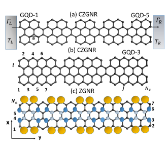
Recent advancements in the in-solution synthesis method have demonstrated the production of graphene nanoribbons featuring cove-shaped zigzag edges [WangX, 13]. These cove-edged ZGNRs (CZGNRs) display adjustable semiconducting phases with varying band gaps [WangX, 13]. While the topological properties of CZGNRs have been explored using first-principle methods [LeeYL, 19] and tight-binding models [Florian, 20], a comprehensive investigation into the electronic structures and transport characteristics of CZGNRs across diverse scenarios, as illustrated in Fig. 1(a) and 1(b), remains incomplete. Our intriguing discovery reveals that the band gaps of CZGNRs depicted in Fig. 1(a) and 1(b) are not dependent on the CZGNR lengths but are determined by the size of individual graphene quantum dots (GQD). Notably, when edge defects are present in CZGNRs, asymmetrical tunneling currents are observed. Saturation currents exhibit limited sensitivity to the CZGNR length but are significantly influenced by the coupling strengths between the electrodes and the CZGNRs. In addition, we examine tunneling currents through GQDs with boron nitride textures within the Coulomb blockade region, revealing the presence of an irregular staircase-like behavior in the tunneling currents.
II Calculation Methodology
To investigate charge transport across the CZGNR coupled to electrodes, we employ a combination of the tight-binding model and the Green’s function technique . The system Hamiltonian is comprised of two components: . Here, denotes the Hamiltonian of the electrodes, encompassing the interaction between the electrodes and the CZGNR. represents the Hamiltonian for the CZGNR and can be expressed as follows[Florian, 20]:
where represents the on-site energy of the orbital in the th row and th column. The operators and create and annihilate an electron at the atom site denoted by (,). characterizes the electron hopping energy from site (,) to site (,). The tight-binding parameters utilized for CZGNRs are for the on-site energy and eV for the nearest-neighbor hopping strength.
The electron currents leaving from the electrodes are given by
| (2) |
where the Fermi distribution function of electrode is denoted as . The chemical potentials ( and , with representing the Fermi energy of the electrodes) depend on the applied bias. The constants , , , and denote the electron charge, Planck’s constant, Boltzmann’s constant, and the equilibrium temperature of the electrodes, respectively.
In the linear response region, the electrical conductance () and Seebeck coefficient () can be computed using and with () defined as
| (3) |
Here, represents the Fermi distribution function of electrodes. signifies the transmission coefficient of a CZGNR connected to electrodes, and it can be calculated using formula [Kuo3, 21,Kuo4, 22], where and denote the tunneling rate (in energy units) at the left and right leads, respectively, and and are the retarded and advanced Green’s functions of the CZGNR, respectively. The tunneling rates are determined by the imaginary part of the self-energy originating from the coupling between the left (right) electrode and its adjacent CZGNR atoms. In terms of tight-binding orbitals, and Green’s functions are matrices. For simplicity, for interface carbon atoms possesses diagonal entries with a common value of . Determining accurately, even using first-principle methods, is challenging [Matsuda, 23]. In this study, we have employed an empirical approach to determine it[Kuo3, 21,MangnusM, 24].
III Results and discussion
III.1 Electronic structures of CZGNRs
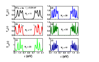
The cove-edged ZGNR (CZGNR) structures with width can be synthesized in reference [WangX, 13], this study focuses on CZGNRs with two widths characterized by and . It’s noteworthy that CZGNRs are generated through periodic removal of some carbon atoms from the upper and lower zigzag edges of ZGNRs (refer to Figures 1(a) and 1(b)). To discuss their relationships, the electron subband structures of ZGNRs with are presented in Figure 2(a). As for the electron subband structures of CZGNRs with , we plot them for varying superlattice constants , defined in terms of the graphene unit cell , as depicted in Figures 2(b)-2(f). It’s important to highlight that within Figure 2(a), the states of the first subband manifest as localized states for values of within the range . Here, is computed as , wherein [Wakabayashi2, 25]. The corresponding eigenvalues of are determined as eV. This finding establishes that states featuring energies within the interval eV correspond to localized edge states, where wave functions exponentially decay in the armchair direction.
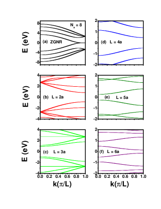
As illustrated in Figures 2(b)-2(f), CZGNRs distinctly exhibit semiconducting phases. Notably, the band gaps of CZGNRs diminish with the increase of . It’s intriguing to observe that each GNR with a brief zigzag segment and a width of can be conceptualized as an independent graphene quantum dot (GQD),which can be characterized by and . The increase in effectively enlarges the GQD sizes. We found that the band gaps of CZGNRs can be determined by the energy level separation of GQD molecules, where and are highest occupied molecule orbital and lowest unoccupied molecule orbital, respectively. Specifically, the computed gap values for CZGNRs are eV, eV, eV, eV, and eV, corresponding to , , , , and , respectively. The role of GQDs plays a charge filter to diminish the energy levels of ZGNRs between the and the . The more detailed discussions will be given in Fig. 4. As seen in Fig. 2(c), distinct flat subbands at eV are discernible. Conversely, for scenarios involving , , and , minute gaps separate the first and second conduction (valence) subbands. Meanwhile, their eV, this indicates that some states near first conduction (valence) subband lower (upper) edges could be localized states. The outcomes depicted in Figure 2(b)-2(f) underscore the tunability of CZGNR band gaps through adjustments in GQD size. Particularly noteworthy is the substantial band gap for instances where ( eV), signifying their potential utility in the realization of nanoscale electronics and room-temperature ( meV) thermoelectric devices.
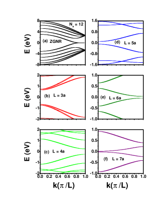
Subsequently, we proceed to evaluate the electronic subband profiles of CZGNR with across varying sizes of GQDs, as depicted in Figure 3. Analogously to Figure 2, the subband arrangements of ZGNRs are featured in Figure 3(a). Within the range of , the electronic states manifest as localized modes. Specifically, when , the corresponding energy is calculated as eV. Much like the scenarios illustrated in Figure 2, the band gaps exhibit a diminishing trend with the enlargement of GQD sizes. Notably, it’s observed that the band gaps remain below eV for . This implies that the states near and may be localized states for when . This situation is the same as that of . These localized states are belonging the states of ZGNR with the flat-band structures. The manifested characteristics are revealed in their electron effective masses. A comprehensive overview of the band gaps and electron effective masses for CZGNRs featuring and across diverse values is presented in the subsequent table. The computation of the electron effective mass in the vicinity of each band gap follows the expression , where and are dimensionless quantities. Additionally, and are expressed in terms of the electron mass () and angstroms (), respectively.
| CZGNR | ||||||
|---|---|---|---|---|---|---|
| 3 | 4 | 5 | 6 | 7 | 8 | |
| 1.875 | 0.958 | 0.512 | 0.288 | 0.171 | 0.106 | |
| 0.35 | 0.235 | 0.237 | 0.265 | 0.282 | 0.323 | |
| CZGNR | ||||||
| 3 | 4 | 5 | 6 | 7 | 8 | |
| 1.3 | 0.495 | 0.188 | 0.076 | 0.034 | 0.016 | |
| 0.194 | 0.165 | 0.226 | 0.345 | 0.507 | 0.647 | |
Remarkably, the electron effective masses show an augmentation with increasing when , signifying a trend towards flatter band structures as expands. It’s notable that in reference [WangX, 13], the band gaps and electron effective mass of CZGNRs featuring were computed for and utilizing a first-principles approach (DFT). Specifically, they obtained eV and for , and eV and for . A comparison with the results provided in the table showcases that the band gaps computed through the tight-binding model slightly deviate in a smaller direction compared to the DFT method. In contrast, the electron effective masses derived from the tight-binding method are approximately one-third of those obtained via the DFT method. Although the values of electron effective masses calculated by the tight binding model are not accuracy as those of DFT, tight binding model could provide analytical expression of electronic band structures, which can deeply reveal the mechanism of electronic properties of CZGNRs.[Wakabayashi2, 25]
III.2 Finite CZGNRs
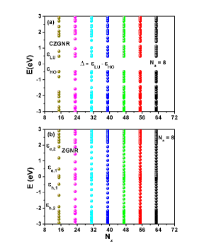
Due to the average size of CZGNRs being nm [WangX, 13], it becomes crucial to elucidate the finite-size effects inherent in CZGNRs. In Figure 4(a), we present computed eigenvalues of CZGNRs with and , as functions of (or ), where signifies the GQD number ranging from 2 to 8. Notably, two eigenvalues, namely and , exhibit a -independent characteristic. Remarkably, a similar intriguing characteristic is also observed at . Additionally, we ascertain that the band gap depicted in Figures 2 and 3 find their determination in .
To gain deeper insights into the attributes of and , we offer the eigenvalues of finite ZGNRs with in Figure 4(b), as functions of , encompassing values such as , and . It emerges that four energy levels, specifically eV, eV, eV, and eV, within the eV range, remain unaffected by variations in . Importantly, it is to be noted that eV and eV.
Despite the consideration of and for in Figure 4, it is pertinent to highlight that analogous situations arise for and . A numerical verification attests that the charge density distribution of a finite ZGNR possessing energy corresponds to that of a CZGNR with when their and exhibit no differences. Notably, the charge density pertaining to in a finite ZGNR with and is depicted in Figure 1(c). In summation, our deduction postulates that (or ) embodies one of the eigenstates of the ZGNR, featuring a specific wave function marked by nodes at vacancy sites that correspond to the periodic removal of carbon atoms from the zigzag edges. Upon satisfying , it is reasonable to infer that the states of CZGNRs in proximity to manifest as localized edge states with interesting magnetic order[SonYW, 26].
III.3 Transport properties of CZGNRs in the linear response region
When graphene interfaces with metal electrodes, the characteristics of the contact, such as the Schottky barrier or ohmic behavior, along with the contact geometries, wield substantial influence over the electron transport phenomena within graphene [Matsuda, 23]. Illustrated in Figure 5 is the computed transmission coefficient of CZGNRs with and , showcasing diverse values at eV. This value aligns with the coupling strength of or metallic electrodes [Matsuda, 23]. For , the transmission coefficients reveal electron transport marked by molecular-like traits, as each resonant energy level is distinctly resolved. Notably, in the scenario where , the pronounced broadening of and due to the interaction between the electrodes and CZGNRs is striking. This broadening phenomenon of resonant levels diminishes as the CZGNR size increases. At instances where two energy levels closely approach each other, they contribute to a transmission coefficient magnitude surpassing unity.
For , the probabilities of transport for and exhibit a decline with the enlargement of . While the spectral intensity of finite CZGNRs proves sensitive to shifts in , it’s noteworthy that the charge blockade region, defined by , remains relatively insensitive to the variation of , a trend congruent with Figure 4(a). The transmission coefficients showcased in Figure 5 furnish insight into the electrical conductance of CZGNRs at absolute zero temperature. Specifically, , where the quantum conductance is expressed as .
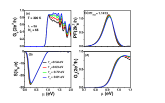
For the potential applications of nanoscale energy harvesting [KuoDMT, 27,Xu, 28], we present the computed electrical conductance (), Seebeck coefficient (), and power factor () as functions of chemical potential values () for distinct values, all considered at the room temperature of K, as illustrated in Figure 6. The range of spans from eV to eV, effectively representing various metallic electrode materials such as , , , and , respectively. In this context, the units for , , and are pegged to , , and . In the depicted graph, Figure 6(a) specifically, it becomes evident that the electrical conductance of subband states () experiences enhancement with increasing , while the of subband edge states in proximity to witnesses suppression (as observed in the curve of Figure 6(d)). Notably, the Seebeck coefficient () close to demonstrates -independent behavior, adhering to , wherein , as portrayed in Figure 6(b). As the analysis continues, Figure 6(c) reveals that the maximum power factor () occurs at eV and is numerically determined as . It’s worth noting that this maximum value approaches a significant milestone, reaching up to of the theoretical limit, , as established for one-dimensional (1D) systems [Whitney, 29].
III.4 Transport properties of CZGNRs in the nonlinear response region
Prior theoretical studies have demonstrated that edge defects can significantly reduce the electron conductance of ZGNRs [Areshkin, 30, Martins, 31]. In this study, we investigate how defects at the edges influence the electron transport properties of CZGNRs by introducing energy shifts on designated defect sites. could be positive or negative, depending on the type of defect [Martins, 31]. The larger the orbital energy shift, the stronger the effect on the electrical conductance [LiTC, 32]. Here, we consider the case of a negative and large to investigate the effects of defects on the electron transport of CZGNRs.
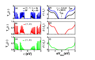
As seen in Fig. 7(a), (b), and (c), the defects occurred at edge sites , , and significantly influence electron transmission coefficients when one compares these transmission coefficients with that of the defect-free (DF) situation. In the absence of defects, there exist 7 resonant channels in the first conduction and valence subbands, respectively. The asymmetrical characteristics of tunneling currents are observed in the presence of defects as shown in Fig. 7(d), (e), and (f). In particular, the tunneling current dramatically drops for the defect at site . This position-dependent defect effect can be understood by their local density of states (LDOS) of CZGNRs with defect-free. The site has a remarkable LDOS, which is why such a defect shows a considerable effect on the tunneling current. If defects occur in the interior sites with small charge densities, their effects on the tunneling current are weak (not shown here). In the case of a defect-free scenario, we define two distinct regions: the tunneling current cut-off region (CR), denoted as , and the saturation region (SR), denoted as . These regions manifest within the gap regions. Notably, the saturation current approximates to . As mentioned in the introduction, we primarily focus on line-contacted electrodes. A novel technique involving edge-contacted electrodes has been developed [HuangWH, 33]. While surface-contacted electrodes can be readily fabricated from a device perspective, their saturation current outputs for GNR-based devices are limited to values smaller than one [LlinasJP, 34, BraunO, 35].

Next, we examine the impact of different values on the tunneling current of CZGNRs. The transmission coefficients of CZGNRs with dimensions , (with nm), and are displayed for three distinct values in Figure 8(a), (b), and (c). The first subband accommodates 15 resonant energy levels spanning a width of eV, ranging from eV to eV. Each resonance peak appears remarkably narrow. Notably, energy levels further from the conduction subband edge () exhibit lower transmission coefficients. The areas beneath the curves increase as increases. The patterns illustrated in Figure 8(a), (b), and (c) underscore how electron transport through CZGNRs from line-contacted electrodes becomes significantly modulated by the coupling strength denoted as , mirroring the observations in Figure 6.
Shifting our focus to the tunneling currents depicted in Figure 8(d), (e), and (f), they correlate with the curves presented in 8(a), (b), and (c), respectively. An increase in is noticeable with an increase in . The tunneling current in the saturation region at eV is almost identical to the blue curve in Fig. 7(d). This suggests that is less sensitive to variations in the length of CZGNRs when the channel length satisfies nm. In Figure 8(c) and 8(f), an additional curve is included for eV, which is similar to graphene-based electrodes. The corresponding tunneling currents exhibit a linear bias-dependent behavior (Ohmic characteristic). Interestingly, the power outputs of these graphene-based electrodes surpass those of metallic electrodes in the saturation region.
III.5 Tunneling current of GQDs in the Coulomb blockade region
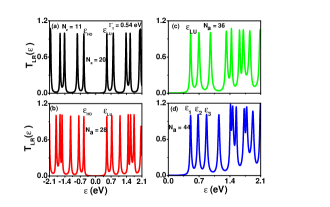
The minimization of transistors with extremely low power consumption is always a significant concern in the semiconductor industry[WangHM, 16,ChiuKL, 36]. As a result, several studies have begun to focus on electron transport through topological states of finite armchair graphene nanoribbons and heterostructures in the Coulomb blockade region [Kuo1, 17,Kuo2, 18,HuangWH, 33]. Here, we propose the implementation of single-electron transistors (SETs) utilizing the schematic structure depicted in Fig. 9(a), which differs significantly from the scenarios involving finite AGNRs found in references [Kuo1, 17,Kuo2, 18,HuangWH, 33]. In Fig. 9(a), GQDs with dimensions and are connected to metallic electrodes via boron-nitride (BN) barriers. It is worth noting that AGNRs with a width of exhibit very narrow energy gaps. However, when AGNRs are confined by BN nanoribbons (BNNRs) [DingY, 37–GSSeal, 39], they display semiconducting properties. To the best of our knowledge, there has been limited investigation into the charge transport through the upper and bottom zigzag edge segments illustrated in Fig. 9(b). Furthermore, BNNRs serve a dual role as both barriers and topological protectors for the localized zigzag edge states.
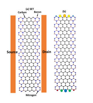
For the sake of simplicity in our analysis, we have disregarded variations in electron hopping strengths between different atoms due to their relatively minor differences [GSSeal, 39]. Specifically, we have assigned energy levels of eV, eV, and eV to boron, nitride, and carbon atoms, respectively. In Fig. 10, we present the computed transmission coefficients for GQDs with BN textures at various values of , while keeping and eV . Notably, a key observation is that eV remains independent of changes in (indicating a lack of size fluctuations along the armchair edge direction). Such robustness is advantageous for the practical implementation of SETs. The charge density distributions corresponding to eV and eV are depicted in Fig. 9(b). As evident from Fig. 9(b), the charge density associated with () is predominantly confined to the upper (bottom) zigzag segment. This observation suggests that achieving charge transport through these zigzag edge segments is challenging when the electrodes are connected to the zigzag edges of GQDs with BN textures.
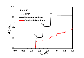
To investigate charge transport within the Coulomb blockade region, both first-principle methods like DFT [SonYW, 26,CaoT, 40] and the tight-binding approach [Kuo3, 21,Kuo4, 22] encounter technical challenges. In our study, we have constructed an effective Hamiltonian that accounts for multiple energy levels and electron Coulomb interactions [Kuo6, 41]. Specifically, we consider an effective Hamiltonian comprising three energy levels denoted as eV, eV, and eV, as shown in Fig. 10(d). Intra-level electron Coulomb interactions are parameterized as eV, eV, and eV, while inter-level Coulomb interactions are given by eV, eV, and eV. These electron Coulomb interactions are determined by the charge densities of the energy levels[Kuo1, 17,Kuo2, 18].
In Fig. 11, we present the computed tunneling current within the Coulomb blockade region. In contrast to the uniform staircase pattern observed in the absence of interactions, we observe an irregular staircase behavior of tunneling current due to electron Coulomb interactions. The plateaus of these staircases result from the interplay between energy level spacing and electron Coulomb interactions. When , complex current spectra emerge as a consequence of these interactions. The heights of the staircases represent the magnitude of probability for each tunneling channel. The probability associated with is primarily influenced by , where the single-particle occupation number for small effective tunneling rate . For , this explains why the tunneling current through is reduced by 1/3 within the Coulomb blockade region compared to the non-interaction case. It’s worth noting that the staircase behavior of tunneling current is destroyed in the presence of a large . This underscores the need for high contact resistances in SETs.
IV Conclusion
The electronic subband structures of cove-edged zigzag graphene nanoribbons (CZGNRs) have been systematically explored under various conditions using the tight-binding model. Similar to semiconducting armchair graphene nanoribbons, CZGNRs exhibit adjustable band gaps and widths, expanding the range of promising options in the field of graphene-based optoelectronics and electronics applications [WangHM, 16, BraunO, 35].
CZGNRs can be envisioned as interconnected GQDs. The band gaps in CZGNRs are determined by the energy level difference , where and represent the energy levels of the highest occupied molecular orbital and the lowest unoccupied molecular orbital of GQDs exhibiting molecular-like characteristics. Significantly, the and values in GQDs originate from distinct eigenstates of finite ZGNRs. The noticeable increase in the effective electron mass within CZGNRs, as GQD sizes grow, suggests that the curvature of the conduction subband edge increasingly resembles flat band-like characteristics.
Moreover, we have explored the optimization of the power factor () for CZGNRs at room temperature. Through an investigation of CZGNRs with parameters , , and , we have achieved a remarkable . This achievement approaches of the theoretical limit set by 1D systems, i.e., . When edge defects are introduced in CZGNRs, we observe intriguing asymmetrical tunneling currents, coupled with a significant reduction in the tunneling magnitude. The tunneling current in the saturation region is found to be less sensitive to variations in the length of CZGNRs () when nm, but it is notably affected by the coupling strengths between the electrodes and the CZGNRs. Additionally, we analyze the tunneling current spectra through GQDs with BN textures, revealing significant Coulomb interactions in the energy level of . This indicates the potential utility of the zigzag edge segments of GQDs with BN textures for the realization of single electron transistors.
Acknowledgments
This work was supported by the National Science and Technology
Council, Taiwan under Contract No. MOST 107-2112-M-008-023MY2.
E-mail address: mtkuo@ee.ncu.edu.tw
References
- (1) K. S. Novoselov, A. K. Geim, S. V. Morozov, D. Jiang, Y. Zhang, S. V. Dubonos, I. V. Grigorieva and A. A. Firsov, Electric field effect in atomically thin carbon films, Science 306 666 (2004).
- (2) J. Cai, P. Ruffieux, R. Jaafar, M. Bieri, T. Braun, S. Blankenburg, M. Muoth, A. P. Seitsonen, M. Saleh, X. Feng, K. Mullen and R. Fasel, Atomically precise bottom-up fabrication of graphene nanoribbons, Nature 466 470 (2010).
- (3) J. Z. Liu, B. W. Li, Y. Z. Tan, A. Giannakopoulos, C. Sanchez-Sanchez, D. Beljonne, P. Ruffieux, R. Fasel, X. L. Feng and K. Mullen, Toward Cove-Edged Low Band Gap Graphene Nanoribbons, J. Am. Chem. Soc. 137 6097 (2015).
- (4) Y. C. Chen, T. Cao, C. Chen, Z. Pedramraz, D. Haberer, D. G. de Oteyza, R. Fischer, S. G. Louie and M. F. Crommie, Molecular bandgap engineering of bottom-up synthesized graphene nanoribbon heterojunctions, Nat. Nanotechnol. 10 156 (2015).
- (5) P. Ruffieux, S. Wang, B. Yang, C. Sachez-Sachez, J. Liu, T. Dienel, L. Talirz, P. Shinde, C. A. Pignedoli, D. Passerone, T. Dumslaff, X. Feng ,K. Mullen and R. Fasel, On-surface synthesis of graphene nanoribbons with zigzag edge topology, Nature 531 489 (2016).
- (6) O. Groning, S. Wang, X. Yao, C. A. Pignedoli , G. B. Barin, C. Daniels, A. Cupo, V. Meunier, X. Feng, A. Narita, K. Muellen, P. Ruffieux and R. Fasel, Engineering of robust topological quantum phases in graphene nanoribbons, Nature 560 209 (2018).
- (7) D. J. Rizzo, G. Veber, T. Cao, C. Bronner, T. Chen, F. Zhao, H. Rodriguez, S. G. Louie, M. F. Crommie and F. R. Fischer, Topological band engineering of graphene nanoribbons, Nature 560 204 (2018).
- (8) L. H. Yan and P. Liljeroth, Engineered electronic states in atomically precise artificial lattices and graphene nanoribbons, ADVANCES IN PHYSICS: X 4 1651672 (2019).
- (9) A. Narita, Z. Chen, Q. Chen , K. Mullen, Solution on-Surface Synthesis of Structurally Defined Graphene Nanoribbons as a New Family of Semiconductors, Chem. Sci. 10, 964 (2019).
- (10) D. J. Rizzo, G. Veber, J. W. Jiang, R. McCurdy, T. Bronner, T. Cao, T. Chen, S. G. Louie, F. R. Fischer and M. F. Crommie, Inducing metallicity in graphene nanoribbons via zero-mode superlattices, Science 369 1597 (2020).
- (11) Q. Sun, Y. Yan, X. L. Yao, K. Mullen, A. Narita, R. Fasel and P. Ruffieux, Evolution of the Topological Energy Band in Graphene Nanoribbons, J. Phys. Chem. Lett. 12 8679 (2021).
- (12) D. J. Rizzo, J. W. Jiang, D. Joshi, G. Veber, C. Bronner, R. A. Durr, P. H. Jacobse , T. Cao, A. Kalayjian, H. Rodriguez, P. Butler, T. Chen, S. G. Louie, F. R. Fischer and M. F. Crommie , Rationally Designed Topological Quantum Dots in Bottom-Up Graphene Nanoribbons, ACS Nano 15 20633 (2021).
- (13) X. Wang, J. Ma, W. H. Zheng, S. Osella, N. Arisnabarreta, J. Droste, J. Serra, O. Ivasenko, A. Lucotti, D. Beljonne, M. Bonn, X. Y. Liu, M. R. Hansen , M. Tommasini, S. De. Feyter, J. Z. Liu, H. I. Wang and X. L. Feng, Cove-Edged Graphene Nanoribbons with Incorporation of Periodic Zigzag-Edge Segments, J. Am. Chem. Soc. 144 228 (2022).
- (14) K. Nakada, M. Fujita, G. Dresselhaus and M. S. Dresselhaus, Edge state in graphene ribbons: Nanometer size effect and edge shape dependence, Phys. Rev. B 54 17954 (1996).
- (15) K. Wakabayashi, M. Fujita, H. Ajiki and M. Sigrist, Electronic and magnetic properties of nanographite ribbons, Phys. Rev. B 59 8271 (1999).
- (16) H. M. Wang, H. S. Wang, C. X. Ma, L. X. Chen, C. X. Jiang, C. Chen , X. M. Xie, A. P. Li and X. R. Wang, Graphene nanoribbons for quantum electronics, Nat. Rev. Phys. 3 791 (2021).
- (17) D. M. T. Kuo, Effects of Coulomb Blockade on the Charge Transport through the Topological States of Finite Armchair Graphene Nanoribbons and Heterostructures, Nanomaterials 13 1757 (2023).
- (18) D. M. T. Kuo, Thermal rectification through the topological states of asymmetrical length armchair graphene nanoribbons heterostructures with vacancies, Nanotechnology 34 505401 (2023).
- (19) L. Y. Lee, F. Z. Zhao, T. Cao, I. Jisoon and S. G. Louie, Topological Phases in Cove-Edged and Chevron Graphene Nanoribbons: Geometric Structures, Z(2) Invariants, and Junction States, Nano Lett. 18 7274 (2018).
- (20) F. M. Arnold, T. J. Liu, A. Kuc, and T. Heine, Structure-Imposed Electronic Topology in Cove-Edged Graphene Nanoribbons, Phys. Rev. Lett. 129, 216401 (2022).
- (21) D. M. T. Kuo and Y. C. Chang, Contact Effects on Thermoelectric Properties of Textured Graphene Nanoribbons, Nanomaterials 12 3357 (2022).
- (22) D. M. T. Kuo, Effects of metallic electrodes on the thermoelectric properties of zigzag graphene nanoribbons with periodic vacancies, J. Phys.: Condens. Matter 35 305301 (2023).
- (23) Y. Matsuda, W. Q. Deng and III W A Goddard, Contact Resistance for ”End-Contacted” Metal-Graphene and Metal-Nanotube Interfaces from Quantum Mechanics, J. Phys. Chem. C. 114 17845 (2010).
- (24) M. J. J. Mangnus, F. R. Fischer, M. F. Crommie, I. Swart and P. H Jacobse, Charge transport in topological graphene nanoribbons and nanoribbon heterostructures, Phys. Rev. B 105 115424 (2022).
- (25) K. Wakabayashi, K. Sasaki, T. Nakanishi and T. Enoki, Electronic states of graphene nanoribbons and analytical solutions, Sci. Technol. Adv. Mater. 11 054504 (2010).
- (26) Y. W. Son, M. L. Cohen, and S. G. Louie, Energy Gaps in Graphene Nanoribbons, Phys. Rev. Lett. 97, 216803 (2006).
- (27) D. M. T Kuo and Y. C. Chang, Thermoelectric and thermal rectification properties of quantum dot junctions, Phys. Rev. B 81, 205321 (2010).
- (28) Y. Xu, Z. Gan and S. C. Zhang, Enhanced Thermoelectric Performance and Anomalous Seebeck Effects in Topological Insulators, Phys. Rev. Lett. 112 226801 (2014).
- (29) R. S. Whitney, Most Efficient Quantum Thermoelectric at Finite Power Output, Phys. Rev. Lett. 112 130601 (2014).
- (30) D. A. Areshkin, D. Gunlycke, and C. T. White, Ballistic transport in graphene nanostrips in the presence of disorder: Importance of edge effects. Nano Lett. 7, 204 (2007).
- (31) T. B. Martins, A. J. R. da Silva, R. H. Miwa and A. Fazzio, sigma- and pi-defects at graphene nanoribbon edges: Building spin filters. Nano Lett. 8, 2293 (2008).
- (32) T. C. Li and S. P. Lu, Quantum conductance of graphene nanoribbons with edge defects, Phys. Rev. B 77, 085408 (2008).
- (33) W. H. Huang, O. Braun, D. I. Indolese, G. B. Barin, G. Gandus, M. Stiefel, A. Olziersky, K. Mullen , M. Luisier, D. Passerone, P. Ruffieux, C. Schonenberger, K. Watanabe, T. Taniguchi, R. Fasel, J. Zhang, M. Calame and M. L. Perrin, Edge Contacts to Atomically Precise Graphene Nanoribbons, https://doi.org/10.1021/acsnano.3c00782
- (34) J. P. Llinas, A. Fairbrother, G. B. Barin, W. Shi, K. H. Lee , S. Wu , B. Y. Choi , R. Braganza, J. Lear , K. Nicholas, W. W. Choi, C. Chen, Z. Pedramrazi, T. Dumslaff , A. Narita , X. L. Feng , K. Mullen, F. Fischer, A. Zettl, P. Ruffieux, E. Yablonovitch, M. Crommie, R. Fasel and J. Bokor, Short-channel field-effect transistors with 9-atom and 13-atom wide graphene nanoribbons, Nat. Commun. 8, 633 (2017).
- (35) O. Braun, J. Overbeck, M. El Abbassi, S. Kaser, R. Furrer, A. Olziersky, A. Flasby, G. B. Barin , Q. Sun, R. Darawish, K. Mullen, P. Ruffieux, R. Fasel, I. Shorubalko, M. L. Perrin, and M. Calame, Optimized graphene electrodes for contacting graphene nanoribbons, Carbon 184 331 (2021).
- (36) K. L. Chiu and Y. Xu, Single-electron transport in graphene-like nanostructures, Phys. Rep.-ReV. Sect. Phys. Lett. 669, 1 (2017).
- (37) Y. Ding, Y. L. Wang and J. Ni, Electronic properties of graphene nanoribbons embedded in boron nitride sheets, Appl. Phys. Lett,95, 123105 (2009).
- (38) L. J. Ci, L. Song, C. H. Jin, D. Jariwala, D. X. Wu, Y. J. Li, A. Srivastava, Z. F. Wang, K. Storr, L. Balicas, F. Liu and P. M. Ajayan, Atomic layers of hybridized boron nitride and graphene domains, Nat. Mater.,9, 430 (2010).
- (39) G. S. Seal and J. Gou, Bandgap opening in boron nitride confined armchair graphene nanoribbon, Appl. Phys. Lett. 98, 143107 (2011).
- (40) T. Cao, F. Z. Zhao, and S. G. Louie, Topological Phases in Graphene Nanoribbons: Junction States, Spin Centers, and Quantum Spin Chains, Phys. Rev. Lett. 119, 076401 (2017).
- (41) D. M. T. Kuo and Y. C. Chang, Tunneling Current Spectroscopy of a Nanostructure Junction Involving Multiple Energy Levels, Phys. Rev. Lett. 99, 086803 (2007).