Breakdown Performance of Guard Ring Designs for Pixel Detectors in CMOS Technology
Abstract
Silicon pixel sensors manufactured using commercial CMOS processes are promising instruments for high-energy particle physics experiments due to their high yield and proven radiation hardness. As one of the essential factors for the operation of detectors, the breakdown performance of pixel sensors constitutes the upper limit of the operating voltage. Six types of passive CMOS test structures were fabricated on high-resistivity wafers. Each of them features a combination of different inter-pixel designs and sets of floating guard rings, which differ from each other in the geometrical layout, implantation type, and overhang structure. A comparative study based on leakage current measurements in the sensor substrate of unirradiated samples was carried out to identify correlations between guard ring designs and breakdown voltages. TCAD simulations using the design parameters of the test structures were performed to discuss the observations and, together with the measurements, ultimately provide design features targeting higher breakdown voltages.
keywords:
pixel detector , silicon sensor , guard ring , passive CMOS , DMAPS , TCAD simulation , sensor breakdown1 Introduction
The operation of silicon detectors in high energy physics (HEP) experiments usually requires a high reverse bias voltage of the sensors to provide a sufficiently high electric field and a possibly large depletion region to achieve fast charge collection by drift and a high signal-to-noise ratio.
The breakdown of the p-n junction emerges when the local electric field is able to trigger the impact ionisation and avalanche multiplication of charge carriers. With the consequence of a significantly high leakage current or even irreversible damage, such an effect is a limiting factor of the sensor operating voltage. The breakdown voltage is influenced by the doping profile, the geometric design, and the oxide thickness [1], and it is a crucial factor in evaluating the performance of sensors. Floating guard rings were introduced in the late 1960s [2] to increase the surface breakdown voltage of planar junctions. This idea has been implemented in the silicon sensors for HEP and tested from the earlier n-substrate sensors to the current n-in-p structures [1, 3, 4].
Commercial CMOS (Complementary Metal-Oxide Semiconductor) sensor manufacturing technologies offer sensor production with high yield, high throughput, and comparatively low cost on large wafers.
Furthermore, the accessibility of features such as multi-metal layers, polysilicon layers, and metal-insulator-metal (MIM) capacitors offers the possibility to implement special sensor features [5, 6]. Several sensors produced in CMOS technologies have proven to be radiation tolerant up to the requirements of HEP experiments [5, 6, 7, 8]. Such features make the silicon sensor fabricated in commercial CMOS technologies a promising instrument in the HEP experiments to meet the increasing demand for silicon detectors [9].
A comparative study of the impact of guard ring layout, implantation type, the overhang of the guard ring implants, and the potential at the field-plate on the breakdown voltage is presented in this paper. Test structures fabricated in LFoundry [10] CMOS process were investigated via leakage current measurements, and their behaviour was qualitatively contrasted with simulations using the Synopsys Technology Computer-Aided Design (TCAD) [11].
2 The Test Structures
Six different n-in-p passive CMOS test structures were designed and fabricated in 2016 as a part of a multi-project wafer submission. The sensor structure, consisting of p-type and n-type wells, was formed by the implantation processes which are standardly utilised in high-voltage devices. The Czochralski-grown p-type wafer with a foundry-specified typical resistivity of [5] was used as the substrate. Moreover, the chips were available in two thicknesses: without backside processing and with backside p-type doping and a metallisation layer.
2.1 Design
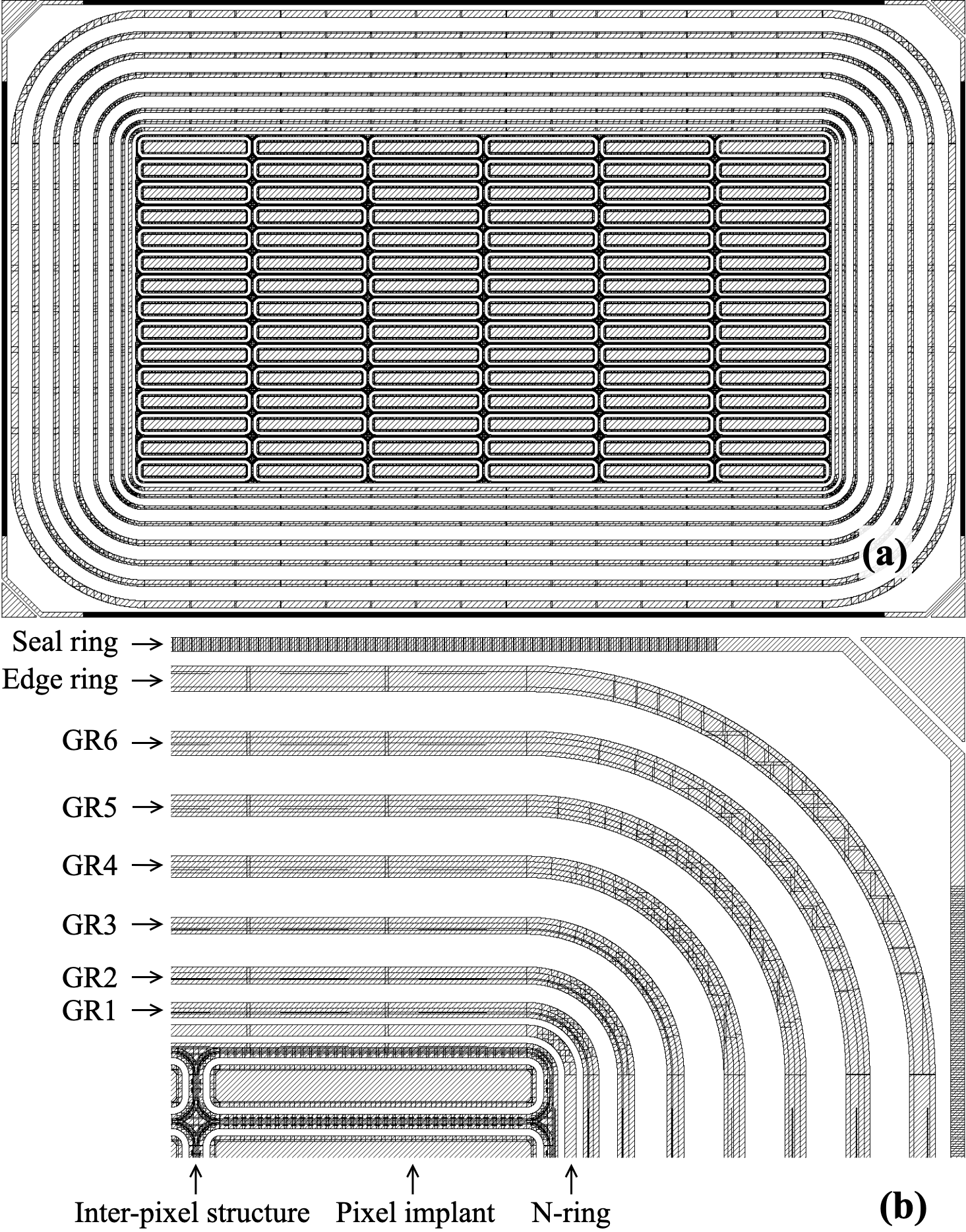
A pixel matrix surrounded by multiple ring structures forms the generic layout of the test structures, as depicted in Figure 1 (a). The pixel matrix region consists of pixel-electrode implants (“Pixel implant”), the inter-pixel structures, and an n-type ring implant (“N-ring”) enclosing the entire matrix structure (Figure 1 (b)). Concentric guard rings (GR) are located between the n-ring and the edge of the test structure. Six different test structures (labelled with letters “A” to “E”, as summarised in Table 1) differ in the number(spacing) of the guard rings, the type of doping used at the guard rings, and the structure at the inter-pixel region.
| Label | Implant | Overhang | # Rings (GR1 Gap) | Inter-pixel structure | Deep n-well |
|---|---|---|---|---|---|
| A | p | Yes | 6 () | p-stop | No |
| B | n+p | Yes | 6 () | p-stop | Yes |
| C | n+p | Yes | 5 () | p-stop | Yes |
| D | p | Yes | 6 () | p-stop | Yes |
| E | n+p | Yes | 5 () | field-plate | Yes |
| F | n+p | No | 5 () | p-stop | Yes |
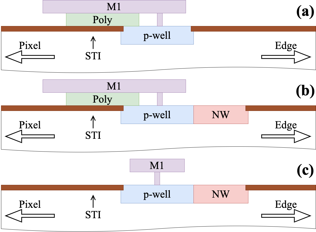
In the pixel matrix region, the test structures differ in the implantation profile of the pixel implants and the inter-pixel structure, as depicted in Figure 2. The CMOS process offers three n-type well implantation profiles with increasing depth: standard n-well “NW” for MOSFET (Metal-Oxide-Semiconductor Field-Effect Transistor) fabrication, the “NISO”, and the “DNW”. These wells are employed to form the pixel implants and the n-ring in two configurations: a standard n-well or a deep n-well combining NW, NISO, and DNW. Moreover, two approaches of the inter-pixel structure were implemented: either a p-well (as in a standard “p-stop”) with two overhang polysilicon (“Poly”) layers that exceed its edges, or a single polysilicon layer (“field-plate”) directly above the Shallow Trench Isolation (“STI”) forming a MOS (Metal-Oxide-Semiconductor) structure.
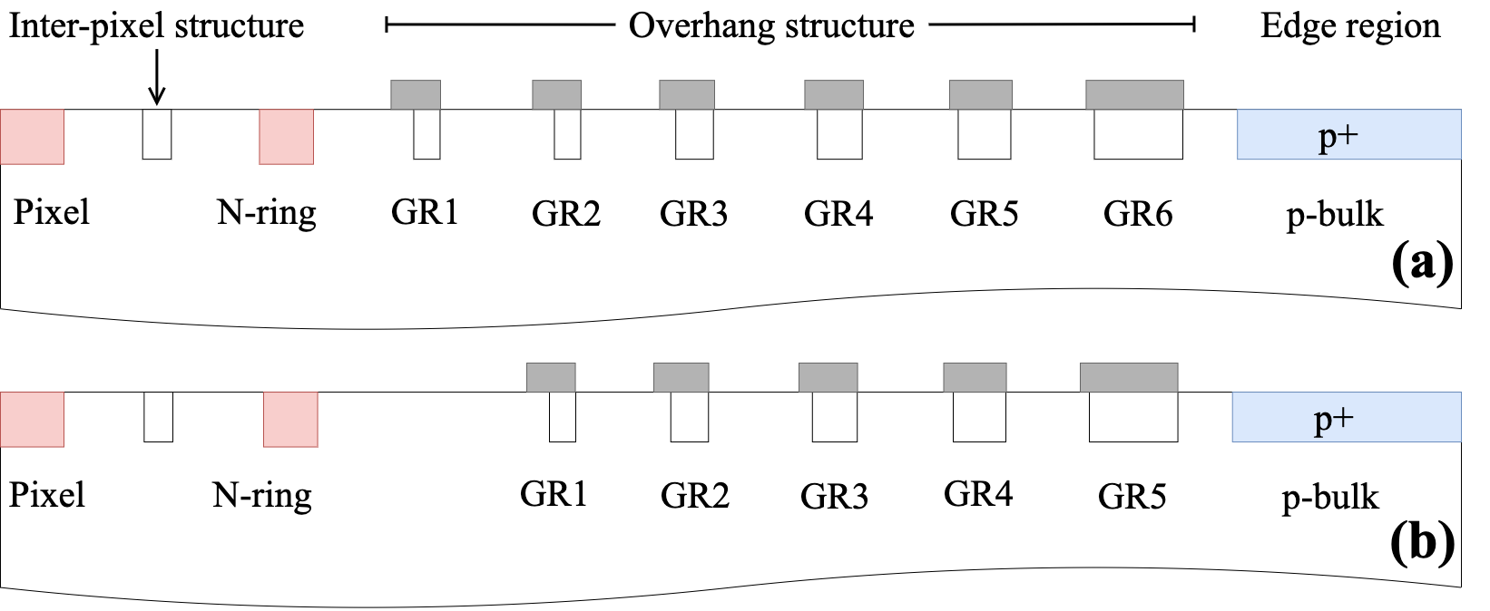
When it comes to the guard rings, the test structures implement multiple designs that differ in the spacing between rings, the type of implant, and the use of polysilicon as an overhang. Figure 3 depicts the generic cross-sections of the guard ring layout, where the version consisting of six guard rings serves as a reference. The version with five guard rings is realised by removing the innermost guard ring, which effectively increases the spacing between the n-ring and the GR1 (GR1 gap). Since the edge ring is electrically connected with the seal ring, both structures are represented by the edge region. Figure 4 depicts three configurations for the guard-ring’s implant and overhang structure adopted in the test structures. The overhang refers to the structures that use the conductive polysilicon and metal layers above the STI to form a MOS structure in the proximity of the guard ring implant. Its effects have been discussed in [3, 13] for silicon sensors with an n-type substrate and in [14] for a p-type substrate CMOS detectors, showing the ability to modify the local potential and electric field strength at the surface of the silicon substrate. Each configuration is applied to all guard rings of the corresponding test structure.
2.2 Samples, Measurement setup and Procedure
Originally, a set of test structures was part of a single die. Two samples (TS1, TS2) with a thickness of were prepared, where TS1 was fully diced so that each structure could be wire-bonded to a PCB. All test structures with a thickness of come from a set of seven different samples (S1-S7) and were not diced to be measured.
Breakdown voltages are determined by identifying the voltage at which a sharp increase in current occurs while scanning the current-voltage behaviour (“I-V curve”) of reverse biased sensors[15].
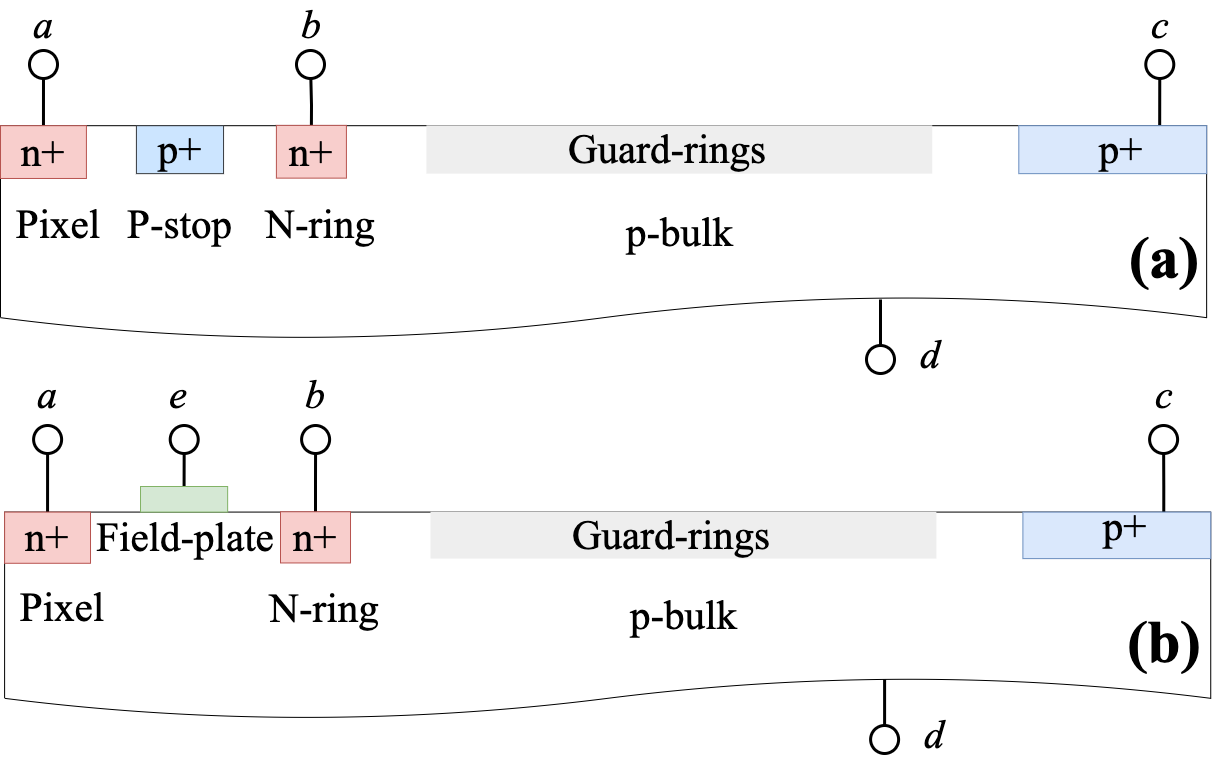
Figure 5 illustrates multiple points where measurements can be performed or voltages can be set to the implants in every test structure.
All and thick samples can be biased from the front side of the sensor [16] by applying a voltage at contact c. Alternatively, the latter ones can be biased from their backside through contact “d”, since they have been processed and metallized after thinning. In any of these cases, the current at the pixel matrix can be measured at contact “a” for two scenarios: 1) a floating n-ring or 2) a n-ring set to the same fixed potential as the pixels. The grounded n-ring scenario represents the designed operation condition of such pixel sensors. The floating n-ring scenario is employed to extend the understanding of the effect from the deep n-well and the field-plate on the breakdown performance. For structure E, an additional voltage can be applied at the polysilicon field-plate via contact e, whereas the p-stop is floating in all other structure designs.
In this work, the leakage current of all test structures was measured while they were frontside-biased. The thick structures were examined with floating n-ring, whereas on the thick structures both the floating and grounded n-ring were measured. For structure E, different potentials were applied at the field-plate.
3 TCAD Simulation for a Qualitative Study
A 2D cross-section of the guard ring region, as Figure 3, was created by simulating the manufacturing process and employed as simulation domain. The resistivity of the sensor bulk was set to , representing a boron doping concentration of approximately , which is within the foundry-specified range. Breakdown simulations of the given guard ring structures were performed using the device simulation tool “Sentaurus Device” [17]. Charge carrier mobility models, such as Masetti doping dependency [18], Canali high-field saturation [19] and Conwell-Weisskopf carrier-carrier scattering [17] were taken into account to describe the complex conditions in the semiconductor sensor. The van Overstraeten impact ionisation model [20] was employed to simulate the avalanche breakdown effect. The Shockley-Read-Hall recombination model [21, 22] with Hurkx tunnelling model [23] was adopted to include the effect of impurities at interface, for unirradiated sensors [24]. For a qualitative study, a set of dummy parameters based on measurements performed on gated-diodes and MOS capacitors [24] was applied to the simulations, since the quantitative characteristics of these test structures are unknown.
4 Measurement Results
4.1 Thick Structures with Floating N-ring
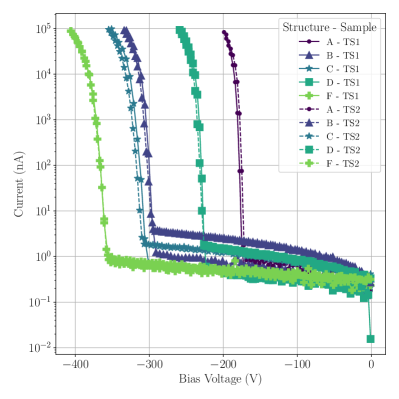
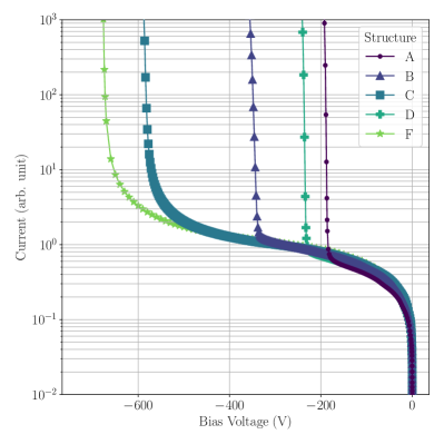
The I-V curves of two different samples of structures A, B, C, D, and F are presented in Figure 6 and the extracted breakdown voltages are listed in Table 2. Both samples provided consistent results, where no influence from the dicing process was observed. The breakdown voltages of the structures ranged from (structure A) to (structure F), indicating a dependence on the guard ring design.
| Label | (V) | Label | (V) | (V) |
|---|---|---|---|---|
| A | ||||
| B | ||||
| C | E | |||
| D | ||||
| F |
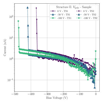
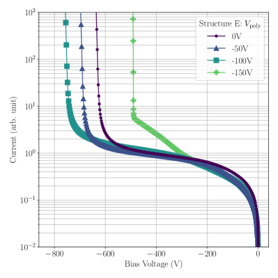
The results of the structure E with fixed potentials at the polysilicon field-plate () are presented in Figure 7 and Table 2. The onset of the breakdown effect was delayed by the increased negative potential between and at the field-plate. Moreover, connecting the field-plate with the bias voltage () led to an earlier breakdown at . For , the breakdown voltage decreased to , and the original behaviour of the sample could not be recovered. A floating field-plate resulted in non-reproducible measurement results.
The test structures were paired in four different groups to determine the impact of individual design features on the breakdown voltage, as presented in Table 3. A higher breakdown voltage was observed for the structures with deep n-implant at pixels and n-ring (Figure 2 (b)), large spacing between n-ring and the first guard ring (Figure 3 (b)), additional n-implant at the guard rings, and the absence of the polysilicon overhang at the guard rings (Figure 4 (c)). Structure E exhibits a possibility of increasing the breakdown voltage by applying an additional negative potential at the field-plate.
| Control Group | Compared Parameter | Condition for higher breakdown voltage |
|---|---|---|
| A & D | Deep implants in the active region | Deep implants at the pixels and n-ring (D) |
| B & C | Size of GR1 gap | Larger spacing between n-ring and GR1 (C) |
| B & D | N-implant at the guard rings | With n-implant at the guard rings (B) |
| C & F | polysilicon overhang | Without polysilicon overhang structure (F) |
4.2 Thick Structures with Floating N-ring
The measurement of breakdown voltages for samples with thickness delivered similar results as for the sensors, as summarised in Table 4. It is noticeable by comparing Table 4 and Table 2 that larger variations of the breakdown voltage were observed for the samples. This was likely due to variations between samples after back-side processing.
| Label | (V) | Label | (V) | (V) |
|---|---|---|---|---|
| A | ||||
| B | ||||
| C | E | |||
| D | ||||
| F |
Measurements of the structure E with on two samples have delivered the same relation between and (Table 4) as observed in the thick samples. A discrepancy of approximately in between both samples results in large variations of the breakdown voltages. Due to the consistent behaviour between the and , as well as the similar leakage current level, this discrepancy is attributed to variations between samples after dicing and back-side processing. Comparing with the results from section 4.1, the consistent relation between guard ring designs (or ) and of structures are independent of the thickness of samples. Therefore, the comparison concerning the control groups in Table 3 still applies.
4.3 Thick Structures with Grounded N-ring
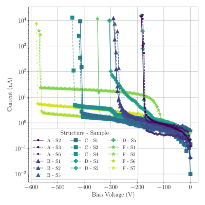
The same set of samples was tested with grounded n-ring for structures A, B, C, D, and F, as illustrated and summarised in Figure 8 and Table 5. Both structures D and F on sample S1 showed a distinct breakdown performance, with respect to the other samples. These two specific measurements were neglected since they are likely caused by production errors unable to be confirmed by the measurements within this work.
An abnormal increase of the leakage current of bias voltage above is observed for structure F from sample S3 and S7. The same effect has occurred in the measurements with floating n-ring. This may be caused by imperfection of the production or the backside processing of the wafer [5, 25]. Nevertheless, the current increase tends to saturate at a certain level, and the breakdown voltage is in accordance with the other samples.
| Label | (V) | Label | (V) | (V) |
|---|---|---|---|---|
| A | ||||
| B | ||||
| C | E | |||
| D | ||||
| F |
With the exception of test structure A, the breakdown voltages measured for all samples with grounded n-ring (Table 5) varied with respect to the measurements with floating n-ring (Table 2). Lower breakdown voltages are observed for structure B and D, revealing a reduction of approximately and , respectively. On the contrary, structure C and F exhibit an increase of breakdown voltage by approximately and , respectively. Nevertheless, the comparison in the control groups (Table 6) mostly agrees with Table 3, except for structure D showing a similar breakdown performance as structure A.
| Control Group | Compared Parameter | Condition for higher breakdown voltage |
|---|---|---|
| A & D | Deep implants in the active region | None (–) |
| B & C | size of GR1 gap | Larger spacing between n-ring and GR1 (C) |
| B & D | N-implant at the guard rings | With n-implant at the guard rings (B) |
| C & F | polysilicon overhang | Without polysilicon overhang structure (F) |
The results in Table 5 indicate that for grounded n-ring the negative potential at the polysilicon field-plate has less influence on the breakdown performance of structure E, in comparison with the floating n-ring scenario. Adding negative voltage at the field-plate, the decrease of the breakdown voltage is only approximately .
4.4 Implementation of the Guard-ring Designs in Other Devices
Guard ring designs similar to those used by the test structures of this work were already implemented in large sensors () fabricated in the same CMOS process. In the prototype of the depleted monolithic active pixel sensor (DMAPS) LF-CPIX [7, 25], two guard ring layouts akin to the one in structure D were employed. The difference between both of them was the spacing between the n-ring and GR1, where one was smaller (with ) and the other one was larger (with ) than the gap used for the test structure. Another DMAPS device LF-Monopix1 [26] adopted a guard ring design based on the structure D of this work, with a gap size larger than that in LF-CPIX. The resulting breakdown voltage was between and [25, 26, 27, 28]. In this case, the influence of the spacing on the breakdown performance was also validated. The successor of the LF-Monopix1, the LF-Monopix2 [29] has a guard ring design close to that of the test structure structure F, which visibly improved its breakdown voltage () [30]. This result is consistent with the breakdown measurements of the test structures, that the additional n-well attached to the floating p-type guard rings improves the breakdown voltage.
5 TCAD Simulation of Breakdown Performances
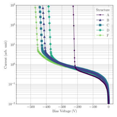
The simulated I-V curves of the test structures A, B, C, D, and F for floating and grounded n-ring are presented in Figures 9 and 10. Since this is merely a 2D simulation of the guard ring region, the results only allow for a qualitative description of the behaviour observed in the actual samples. The extracted breakdown voltages are listed in Table 7, and they reproduced the relative changes in breakdown voltage between structures for both floating or grounded n-ring cases. As observed in the measurements, the reduction of breakdown voltages for structure B (by ) and D (by ), and the increase of the breakdown voltages for structure C (by ) and F (by ) are obtained from the simulation.
| Label | (V) | (V) | Label | (V) | (V) | (V) |
|---|---|---|---|---|---|---|
| A | ||||||
| B | ||||||
| C | E | |||||
| D | ||||||
| F |
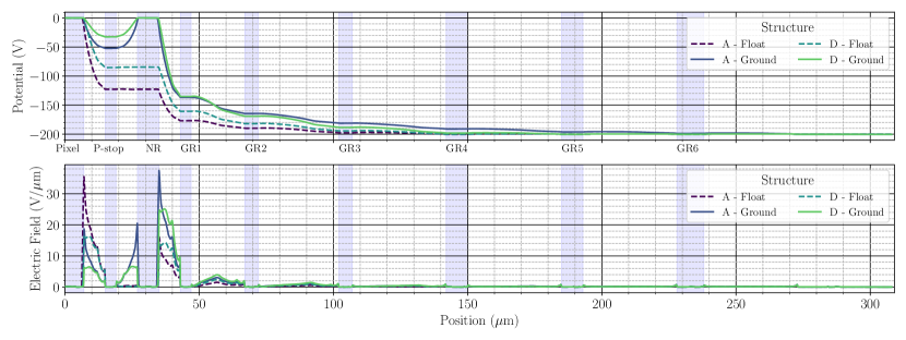
To understand the relation between the breakdown performance and the design features of guard rings, it is helpful to consider the potential and electric field strength distribution across the surface of the guard ring region, because the strength of the impact ionisation and the onset of the junction breakdown are correlated with the magnitude of the electric field. The distributions were obtained at a depth of from the silicon/oxide interface (i.e. the lower boundary of the STI). From these, the maximum electric field (or the largest potential-drop between implants) can be identified and compared across guard ring designs and measurement scenarios. Figure 11 illustrates the extracted distributions for structures A and D with floating and grounded n-ring. For a given bias voltage (e.g. ), the potentials at the floating wells were assigned with different negative potentials based on their distance to the pixel/n-ring. This behaviour resulted in a gradual decrease of the potential from the pixel matrix to the sensor edge. In both guard ring structures, the maximum potential-drop and subsequently the maximum electric field occurred between pixel and p-stop for a floating n-ring, or n-ring and GR1 for a grounded n-ring. The floating n-ring and the p-stop acted as extra guard rings with a similar potential starting from the pixel. The addition of DNW to the n-ring (as in structure D) elevated the potential at the p-stop, hence reduced the maximum potential-drop and, subsequently, the maximum electric field. This can explain the higher breakdown voltage of structure D in comparison with structure A with a floating n-ring. By grounding the n-ring in structure D, the potential at the p-stop is higher than that in the floating n-ring scenario. Moreover, the maximum electric field is shifted to the edge of the n-ring, and increased by approximately . As a result, the breakdown voltage of structure D is reduced after grounding the n-ring. For structure A, although the maximum electric field is relocated in the same manner by grounding the n-ring, the field strength is similar as in the case where it is floating. Therefore, the breakdown voltage was similar for both scenarios.
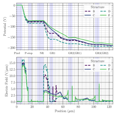
Similar behaviours of the potential and electric field distributions were observed (as depicted in Figure 12) in structures B, C, and F with a floating n-ring, where the most prominent potential drop and the maximum electric field appears between the pixel and the p-stop.
With additional NW attached to the guard rings (structure B), the potentials at the n-ring and guard rings were elevated in comparison with the structure without NW (structure D). The increase in the spacing between the n-ring and GR1 (structures C and F) further smoothed the potential drop in this region, and resulted in a smaller electric field. However, such changes in the guard ring designs only caused small reductions of the maximum electric field. These effects got more pronounced by grounding the n-ring, as can be observed in Figure 13.
The elevation of the potentials at the guard rings and the smoothening of the potential drop visibly reduced the maximum electric field which was relocated to the region between the n-ring and GR1. Consequently, the structure C revealed a significantly higher breakdown voltage than the structures B and D.
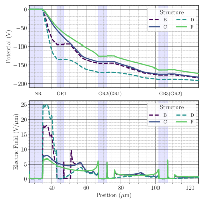
The effect of the overhang structure can be more clearly identified through comparing structure C and F with a grounded n-ring, as depicted in Figure 13. In this case the overhang in structure C causes an overall suppression of the potential at the floating guard rings. Therefore, the maximum electric field at the n-ring of structure C was higher than that in structure F. This ensures a higher breakdown voltage of structure F.
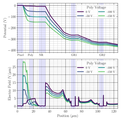
The simulated IV-curves and distributions of structure E with floating n-ring are presented in Figure 14. According to the extracted breakdown voltages listed in Table 7, the simulation qualitatively reproduced the measurements in Table 4. The early breakdown for was predicted by the simulation, as well. As depicted in Figure 15, the potential at the region underneath the field-plate was affected by the set . The field-plate, the underlying silicon oxide, and the silicon substrate forms an MOS structure, where the field-plate acts as the gate (see Figure2 (c)). The negative voltage applied to the field-plate determines the potential at the surface of the silicon substrate. During the ramp of bias voltage, the potential in this region was lowered and finally stabilised at approximately . For , the maximum electric field was located at the n-ring, which indicates the location of the junction breakdown. As was increased, the electric field was reduced at the n-ring and increased at the pixel implant. Adding the bias voltage increased the potential difference and the electric field mainly between the n-ring and GR1 until the onset of breakdown occurs. This gave the result, that the breakdown voltage was lower for than , due to the higher electric field at the n-ring. Nevertheless, when the potential beneath the field-plate reached approximately , the electric field was already large enough to trigger the junction breakdown at the pixel implant. Thus the onset of the breakdown occurred at the pixel for a lower bias voltage, in comparison with other settings. By grounding the n-ring, the breakdown voltages revealed a less significant response to the change in the (Table 7). In this case, the maximum electric field was located at the n-ring, which was predominately determined by the bias voltage and less influenced by the potential at the field-plate.
It should be noticed that the results in this work were obtained and discussed based on unirradiated sensors, so that they cannot be directly extrapolated to the cases of radiation damages. Especially for the effects of the overhang structure and field-plate, where MOS structures are involved, the results can be substantially different, due to the radiation-induced changes on the electrical properties at the - interface. Therefore, the behaviour of the breakdown performance of guard ring structures after considering radiation damages requires a dedicated study.
6 Conclusion
Measurements of the current-voltage behaviour were performed on unirradiated passive CMOS test structures fabricated on high resistivity p-type substrate for characterising their breakdown performances. By using 2D TCAD simulations of the guard ring region, the relation between multiple design features and the breakdown voltage were qualitatively reproduced, and discussed based on the simulated potential and electric field distribution. These comparative studies showed that geometrical layouts, implant types, and overhang structures of the floating guard rings determine the strength of the maximum electric field in the guard ring region, and hence the breakdown voltage. From the perspective of the implant geometry and type, the breakdown voltage of an unirradiated sensor can be improved by:
-
1.
An increase in the spacing between the n-ring and the first guard ring:
A large spacing reduces the steepness of the maximum potential-drop in the guard ring region. -
2.
The use of adjacent n-type and p-type implants as guard rings:
Attaching an n-well to the p-type guard ring implant elevates the potential of the floating guard ring, thus smooths the potential distribution and reduce the maximum electric field. This effect can be further enhanced by the use of deep n-wells.
The use of an overhang structure and the field-plate exhibits the modification to the potential distribution via MOS structures. It is found that implementing the overhang structure considered in this work can cause an increase in the maximum electric field, and hence, reduce the breakdown voltage of unirradiated sensors. Assigning different voltages at the poly silicon field-plate can be used to modify the breakdown voltage, since it can control the potential in the corresponding region and alter the maximum electric field in the sensor. Moreover, future studies are foreseen to explore the implementation of the deep n-wells and the field-plates in the guard ring structure to achieve further improvements of the breakdown performances.
7 Acknowledgements
This work has received funding from the Deutsche Forschungsgemeinschaft DFG (grant WE 976/4-1), the German Federal Ministry of Education and Research BMBF (grant 05H15PDCA9) and the European Union’s Horizon 2020 Research and Innovation programme under grant agreements No. 675587 (STREAM), 654168 (AIDA-2020) and 101004761 (AIDA-Innova).
References
- [1] O. Koybasi, G. Bolla, D. Bortoletto, Guard Ring Simulations for n-on-p Silicon Particle Detectors, IEEE Transactions on Nuclear Science 57 (5) (2010) 2978–2986. doi:10.1109/TNS.2010.2063439.
- [2] Y. Kao, E. Wolley, High-voltage planar p-n junctions, Proceedings of the IEEE 55 (8) (1967) 1409–1414. doi:10.1109/PROC.1967.5842.
- [3] L. Rossi, P. Fischer, T. Rohe, N. Wermes, Pixel detectors: From fundamentals to applications, Springer Science & Business Media, 2006.
- [4] M. Benoit, A. Lounis, N. Dinu, Simulation of guard ring influence on the performance of ATLAS pixel detectors for inner layer replacement, J. Instrum. 4 (03) (2009) P03025. doi:10.1088/1748-0221/4/03/p03025.
-
[5]
D.-L. Pohl, et al.,
Radiation hard pixel
sensors using high-resistive wafers in a 150 nm CMOS processing line, J.
Instrum. 12 (06) (2017) P06020.
doi:10.1088/1748-0221/12/06/p06020.
URL http://dx.doi.org/10.1088/1748-0221/12/06/P06020 - [6] Y. Dieter, et al., Radiation tolerant, thin, passive CMOS sensors read out with the RD53A chip, Nucl. Instrum. Methods Phys. Res. A 1015 (2021) 165771. doi:https://doi.org/10.1016/j.nima.2021.165771.
- [7] T. Hirono, et al., Depleted fully monolithic active CMOS pixel sensors (DMAPS) in high resistivity 150 nm technology for LHC, Nucl. Instrum. Methods Phys. Res. A 924 (2019) 87 – 91, 11th International Hiroshima Symposium on Development and Application of Semiconductor Tracking Detectors. doi:https://doi.org/10.1016/j.nima.2018.10.059.
- [8] M. Barbero, et al., Radiation hard DMAPS pixel sensors in 150 nm CMOS technology for operation at LHC, J. Instrum. 15 (05) (2020) P05013. doi:https://doi.org/10.1088/1748-0221/15/05/p05013.
- [9] M. Garcia-Sciveres, N. Wermes, A review of advances in pixel detectors for experiments with high rate and radiation, Reports on Progress in Physics 81 (6) (2018) 066101. doi:http://dx.doi.org/10.1088/1361-6633/aab064.
- [10] LFoundry [online]. http://www.lfoundry.com [cited 16.11.2022].
- [11] Synopsys TCAD [online].
-
[12]
S.-H. Chen, M.-D. Ker,
Investigation
on seal-ring rules for IC product reliability in 0.25- CMOS
technology, Microelectronics Reliability 45 (9) (2005) 1311–1316,
proceedings of the 16th European Symposium on Reliability of Electron
Devices, Failure Physics and Analysis.
doi:https://doi.org/10.1016/j.microrel.2005.07.012.
URL https://www.sciencedirect.com/science/article/pii/S0026271405001629 - [13] B. S. Avset, L. Evensen, The effect of metal field plates on multiguard structures with floating p+ guard rings, Nucl. Instrum. Methods Phys. Res. A 377 (2) (1996) 397–403, proceedings of the Seventh European Symposium on Semiconductor. doi:https://doi.org/10.1016/0168-9002(96)00194-5.
-
[14]
T. Hemperek,
Exploration of
advanced CMOS technologies for new pixel detector concepts in High Energy
Physics, Ph.D. thesis, Rheinischen Friedrich-Wilhelms-Universität Bonn
(April. 2018).
URL https://nbn-resolving.org/urn:nbn:de:hbz:5n-50354 - [15] S. M. Sze, K. K. Ng, Physics of Semiconductor Devices, John Wiley & Sons, Inc., 2007.
- [16] M. Baselga, et al., Front-side biasing of n-in-p silicon strip detectors, Journal of Instrumentation 13 (11) (2018) P11007. doi:10.1088/1748-0221/13/11/p11007.
-
[17]
Synopsys, Sentaurus™ Device User
Guid, www.synopsys.com (June 2015).
URL www.synopsys.com - [18] G. Masetti, M. Severi, S. Solmi, Modeling of carrier mobility against carrier concentration in arsenic-, phosphorus-, and boron-doped silicon, IEEE Transactions on Electron Devices 30 (7) (1983) 764–769. doi:10.1109/T-ED.1983.21207.
- [19] C. Canali, et al., Electron and hole drift velocity measurements in silicon and their empirical relation to electric field and temperature, IEEE Transactions on Electron Devices 22 (11) (1975) 1045–1047. doi:10.1109/T-ED.1975.18267.
-
[20]
R. Van Overstraeten, H. De Man,
Measurement of the
ionization rates in diffused silicon p-n junctions, Solid-State Electronics
13 (5) (1970) 583–608.
doi:10.1016/0038-1101(70)90139-5.
URL http://dx.doi.org/10.1016/0038-1101(70)90139-5 - [21] W. Shockley, Statistics of the Recombinations of Holes and Electrons, Physical Review 87 (5) (1952) 835–842. doi:10.1103/PhysRev.87.835.
-
[22]
R. N. Hall,
Electron-Hole
Recombination in Germanium, Phys. Rev. 87 (1952) 387–387.
doi:10.1103/PhysRev.87.387.
URL https://link.aps.org/doi/10.1103/PhysRev.87.387 - [23] G. A. M. Hurkx, D. B. M. Klaassen, M. P. G. Knuvers, A new recombination model for device simulation including tunneling, IEEE Transactions on Electron Devices 39 (2) (1992) 331–338. doi:10.1109/16.121690.
- [24] A. Morozzi, et al., TCAD Modeling of Surface Radiation Damage Effects: A State-Of-The-Art Review, Frontiers in Physics 9. doi:10.3389/fphy.2021.617322.
-
[25]
T. Hirono, Development of
depleted monolithic active pixel sensors for high rate and hagh radiation
experiments at HL-LHC, Ph.D. thesis, Rheinischen
Friedrich-Wilhelms-Universität Bonn, Nussallee 12, D-53115 Bonn (2019).
URL http://hdl.handle.net/20.500.11811/7933 - [26] T. Wang, et al., Depleted Monolithic Active Pixel Sensors in the LFoundry 150 nm and TowerJazz 180 nm CMOS Technologies, in: Proceedings of The 28th International Workshop on Vertex Detectors —PoS(Vertex2019), Sissa Medialab, 2020. doi:https://doi.org/10.22323/1.373.0026.
-
[27]
T. Wang, et al.,
Depleted fully
monolithic CMOS pixel detectors using a column based readout architecture for
the ATLAS Inner Tracker upgrade, J. Instrum. 13 (03) (2018) C03039.
doi:10.1088/1748-0221/13/03/c03039.
URL http://dx.doi.org/10.1088/1748-0221/13/03/C03039 - [28] F. Iguaz, et al., Characterization of a depleted monolithic pixel sensors in 150 nm CMOS technology for the ATLAS Inner Tracker upgrade, Nucl. Instrum. Methods Phys. Res. A 936 (2019) 652–653, Frontier Detectors for Frontier Physics: 14th Pisa Meeting on Advanced Detectors. doi:https://doi.org/10.1016/j.nima.2018.11.009.
-
[29]
J. Dingfelder, et al.,
Progress
in DMAPS developments and first tests of the Monopix2 chips in 150 nm
LFoundry and 180 nm TowerJazz technology, Nuclear Instruments and Methods
in Physics Research Section A: Accelerators, Spectrometers, Detectors and
Associated Equipment 1034 (2022) 166747.
doi:https://doi.org/10.1016/j.nima.2022.166747.
URL https://www.sciencedirect.com/science/article/pii/S0168900222002674 - [30] I. Caicedo, et al., (In Press) Improvement in the Design and Performance of the Monopix2 Recticle-Scale DMAPS, JPS Conf. Proc.