A broadband pulse amplifier for Joule heating experiments in diamond anvil cells
Abstract
Decades of measurements of the thermophysical properties of hot metals show that pulsed Joule heating is an effective method to heat solid and liquid metals that are chemically reactive or difficult to contain. In order to extend such measurements to megabar pressures, pulsed heating methods must be integrated with diamond anvil cells. We report the design and characterization of a new pulse amplifier that can heat to m-diameter metal wires to 1000s of kelvin at megabar pressures using diamond anvil cells. Pulse durations and peak currents can each be varied over 3 orders of magnitude, from 5 s to 10 ms and 0.2 to 200 A. The pulse amplifier is integrated with a current probe. Two voltage probes attached to the body of a diamond anvil cell can be used to measure voltage in a four point probe geometry. The accuracy of four point probe resistance measurements for a dummy sample with 0.1 resistance are typically better than at all times from 2 s to 10 ms after the beginning of the pulse.
I Introduction
Continuous laser heating, pulsed laser heating, and continuous Joule heating in diamond anvil cells have been used for a wide variety of melting,Weir et al. (2012); Sinmyo, Hirose, and Ohishi (2019); Parisiades (2021), synthesis,Alabdulkarim et al. (2023) and transport measurementsYagi et al. (2011); Konôpková et al. (2016) up to several megabars of pressure. Until very recently, pulsed Joule heating had not been combined with DACs, despite the success of pulsed laser methods,Yagi et al. (2011); Konôpková et al. (2016); Zaghoo, Salamat, and Silvera (2016) and despite the finite element model results showing it might provide an unambiguous way to detect melting transitions.Geballe and Jeanloz (2012)
In contrast, pulsed Joule heating has been used for decades of groundbreaking measurements on the thermophysical properties of materials heated from ambient pressure to temperatures far above melting.Cagran and Pottlacher (2008); Cezairliyan and McClure (1987); Kondratyev and Rakhel (2019) Typically, a pulse of current with kA amplitude is used to heat a mm-diameter sample to many 1000s of K on the s to ms timescale. Gallob, Jäger, and Pottlacher (1986); Cagran and Pottlacher (2008); Cezairliyan and McClure (1987); Henry et al. (1972) Historically, pulse amplifiers were based on vacuum tube technologies such as triggered spark gaps or ignitrons because of their high current and voltage ratings ( kA, kV).Cook (2000) Typically, two spark gaps were used: one to start the pulse and a second one to end the pulse. Two are required because spark gaps are “semi-controlled” switches, meaning they can only be externally controlled in one direction, on or off. Moreover, each spark gap required a high voltage (kV) trigger, which was typically provided by yet another vacuum tube (e.g. a thyratron), adding complexity to the circuit.Henry et al. (1972); Gallob, Jäger, and Pottlacher (1986)
Recently, we showed that pulses with smaller pulse amplitude (10s of A, 10s of V) can be used to melt platinum samples on the s-timescale at pressures up to 1.1 megabar in diamond anvil cells. Geballe et al. (2021) Because of the relatively low power requirements, we were able to use a simple pulse amplifier circuit based on a “fully-controlled” solid-state switch that was triggered directly from a delay generator. Moreover, the pulse amplifier was small, safe, and robust enough to transport to a synchrotron facility for X-ray measurements synchronized with the Joule heating pulses.
However, three limitations of the pulse amplifier and sensing circuitry were detected during the platinum heating experiments.Geballe et al. (2021) First, the pulse power was limited by the 60 V maximum rating of the N-channel MOSFET around which the amplifier was based. Second, at least one of the instrumentation amplifiers used for current and voltage sensing seemed to become damaged, causing spurious distortions in our final set of measurements (Section S1c of Ref. Geballe et al., 2021). Third, the accuracy of the voltage drop across the sample was mediocre in cases where the sample resistance was much smaller than the series resistance of the MOSFET.
Here, we describe a new pulse amplifier and electrical sensing equipment designed for improved robustness, voltage range, and accuracy of current and voltage measurements during pulsed Joule heating. The crucial new components are a high-side solid state switch and passive probes, rather than the N-channel MOSFET and instrumentation amplifiers used in Ref. Geballe et al., 2021.
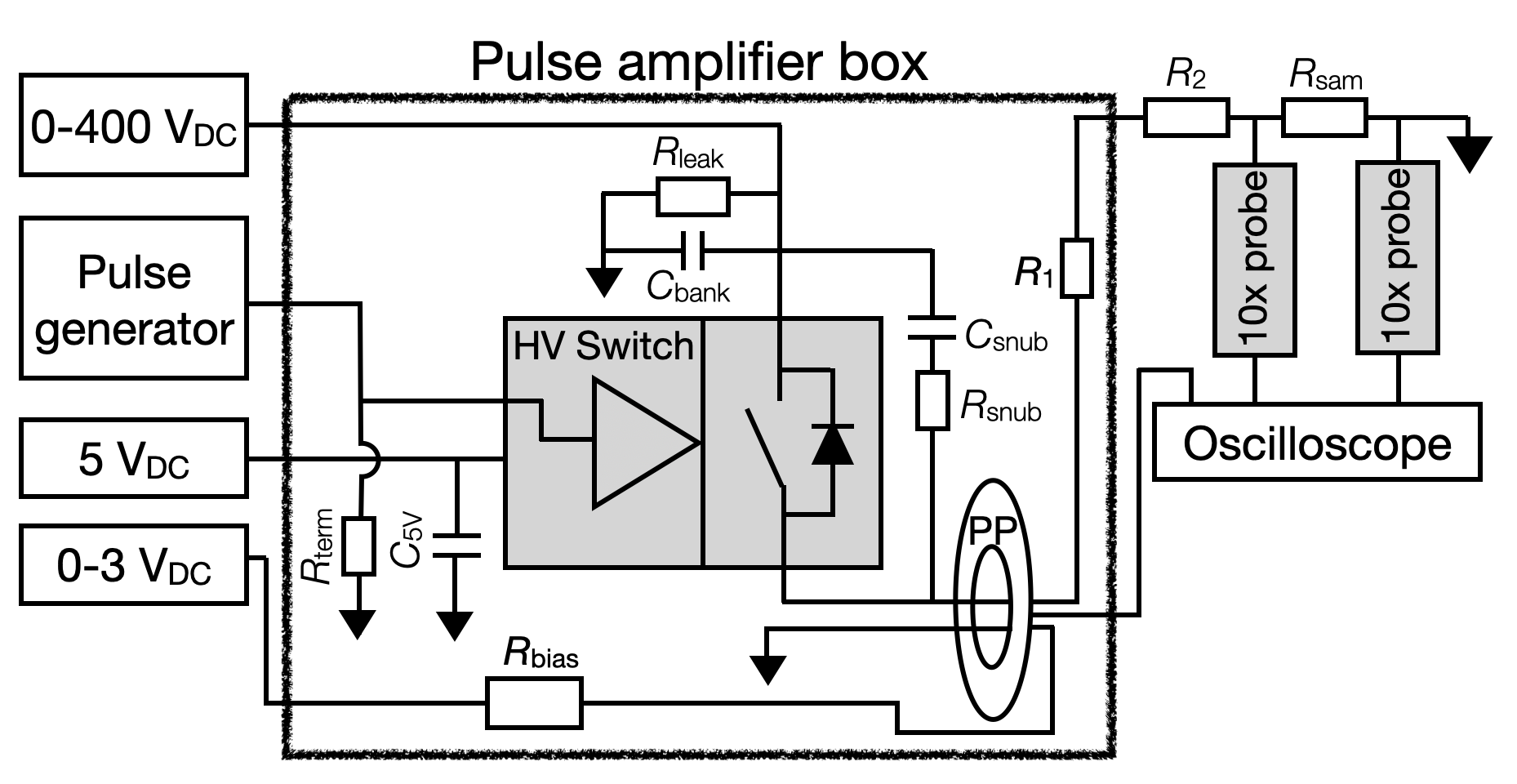
II Electrical Design
The pulse amplifier is designed around the HTS-81-25-B switch from Behlke (Fig. 1). The switch is powered by 5 V and 0.2 A from a regulated DC power supply. A DC power supply charges the primary capacitor, “”, which stores charge at the high voltage side of the switch. When the switch is triggered by a TTL signal (2-5 V amplitude) from a pulse generator, the capacitor is discharged through a series of buffer resistors and through the sample to ground. The first buffer resistor, , is a 1 , 25 W resistor that is hard-wired inside the pulse amplifier box. The second buffer resistor, , is twisted into the delivery leads (Fig. 2b), allowing the user to easily switch between values of . The data presented here uses or 3 . The discharge is cut off when the TTL signal ends. The natural decay timescale of the capacitor discharge is F, which equals 70 s for and 280 s for . In other words, the pulse current decays exponentially to the maximum current of the DC power supply in 100s of s.
Electrical sensing relies on three passive probes: a broadband current monitor (also known as a “Pearson probe”; labeled “PP”), and two 10x oscilloscope probes. Part numbers are listed in 1. The Pearson probe outputs a voltage to the oscilloscope that is equal to 0.1 times the current. Hence, the oscilloscope measures , , and , where and are four point probe voltages at the high side and low side of sample, respectively. (After collecting the data for this manuscript, a third voltage probe was added to monitor voltage at the output of the pulse amplifier box, which is convenient for monitoring resistance in a two point probe configuration.)
Note that the use of a high-side switch enables the use of a passive voltage probe to measure accurate values of . If we had used a low-side switch and passive voltage probes, each probe would measure the voltage of interest plus the voltage drop across the switch, which is often much larger than the voltage of interest. For example, if the switch’s series resistance is 1 and the high pressure metal sample’s resistance is m, a 1% error in measurement of or propagates to % error in .
Two additional components help avoid saturation of the electrical measurements at high current and voltage. First, if the integral of current over time exceeds Amp-seconds for a single pulse, Pearson probe Model 411 saturates according to the manufacturer’s specification sheet. To extend the time-current integral for the highest current pulse presented here, we follow the manufacturer’s recommendation to run 0.1 A of continuous direct current in the reverse direction through a very simple circuit that consists of a DC power supply and a 3 resistor labeled “”. Second, if the Pearson probe’s output voltage exceeds the 50 V range of the oscilloscope, we add a 10 dB attenuator at the oscilloscope input.
Additional resistors and capacitors are added to the pulse amplifier to damp oscillations. A 47 resistor labeled “” in Fig. 1 terminates the output from the pulse generator. A 10 F capacitor buffers the 5 V DC power supply. A capacitor and resistor in series create a low-pass filter, which damps high frequency oscillations that would otherwise oscillate across the switch when it is turned on and off. They are labeled “” and “”. Their product, F ns is the low pass filter timescale.
Finally, two features are added for safety purposes. First, a 250 k resistor, “”, drains the capacitor “” in the characteristic time seconds. Second, a panel-mount voltmeter monitors the voltage on the high side of the capacitor. The voltmeter is shown in the photo in Fig. 2a, but not in the schematic.
III Mechanical Design and Construction
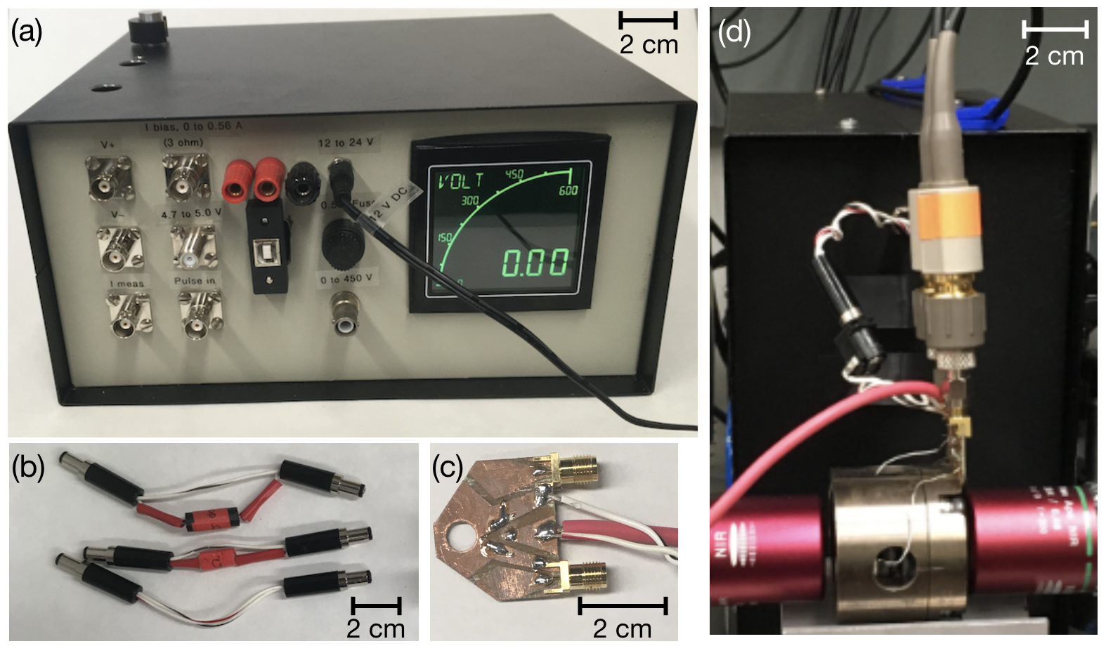
A 25 x 20 x 13 cm metal box houses a circuit board that is held on four standoffs. Five elements are attached by screws to the circuit board: the Pearson probe, the HV switch, and three power resistors (, and ).The primary capacitor, , is pressed into through holes and soldered. The other elements are attached by solder. The faces of the box hold the panel-mount voltmeter, panel-mount BNC connectors for connections with the DC power supplies, pulse generator, and oscilloscope, and a panel-mount barrel connector that connects to and to the pulse amplifier. The oscilloscope probes are fastened onto a face of the box for strain relief.
IV Results
IV.1 100 m dummy sample
The pulse amplifier is tested with m and or 3 . The 100 m dummy sample is Ohmite brand, part number WHER10FET. It has a 5 W power rating and a nominal precision of 1% in resistance, which we confirm by measurement with a Keithley Sourcemeter 2400 before and after pulsing high amplitude currents through it. Single pulses are used during 100 m dummy testing (i.e. no averaging to reduce noise). The start and end of each pulse is triggered by a pulse generator (Berkeley Nucleonics Model 525).
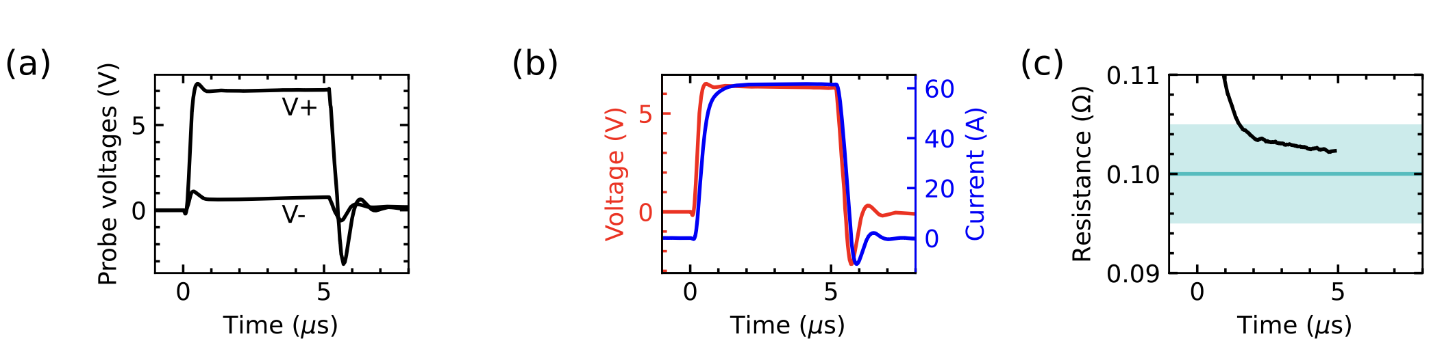
An example of a 5 s pulse using is shown in Fig. 3. The current rises to A with a rise time of 460 s, and drops to 0 A with a fall time of 350 s. Rise time and fall time are defined by time interval between 10% and 90% . Resistance is determined by dividing the four point probe voltage by current. In this example, the accuracy of resistance is better than 5% at all times from 1.4 to 4.9 s.
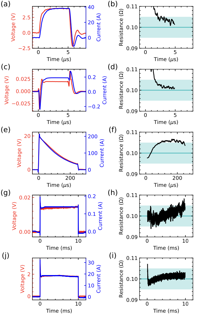
Fig. 4 shows four other tests that demonstrate the range of pulses that can be driven from the pulse amplifier. The pulse amplifier can operate over 3 orders of magnitude in pulse duration and in peak current: 5 s to 10 ms, and 0.2 to 200 A. In almost all cases, resistance measurements are within 5% of the true value at all times from s until the end of the pulse (Fig. 4b,f,h). The main exception is that the error reaches during the highest amplitude pulse (Fig. 4d). Note that to achieve the longest pulses, we used a high current DC power supply (XANTREX XHR 60-18), whereas to achieve relatively short, high voltage pulses we used an SRS PS310 power supply to charge . Also note that if we attempt to end the pulse when current exceeds A, the circuit begins to oscillate wildly; high amplitude 500 kHz oscillations persist for more than 100 s. These oscillations ringing could damage the pulse amplifier or a delicate sample. Hence, the amplitude of the pulse in Fig. 3 cannot be increased without risk, and the duration of the pulse in Fig. 4c cannot be decreased by more than s without risk.
The longest duration pulse that can be measured with high accuracy in our measurement scheme is 10 ms. At longer times, Pearson probe Model 411 approaches its low frequency bandwidth limit. The manufacturer’s specification sheet lists a 0.9 %/ms “droop rate”, and indeed at 10s of ms, the measured current decreases steadily over time by more than 10% even though the voltage measurement remains steady. Numerical correction for the droop rate might be possible if a calibration of droop rate were performed.
Using , the rise time is 1 s. Using , a faster rise time of ns is achieved (Figs. 4a,c). Further increasing to 10 or has no effect on the rise time. The rise time is also sensitive the snubber components (, ). By choosing a smaller values of or , the rise time increases by a small amount, but the stability of the pulse amplifier is reduced. For example, decreasing to 25 nF reduces the rise time to ns, but the rising edge of the pulse includes a few oscillations. For nF, the oscillation amplitude increases further for both the rising edge and the falling edge, and the sharpness of the rising edge is essentially unchanged.
IV.2 Iron sample at high pressure
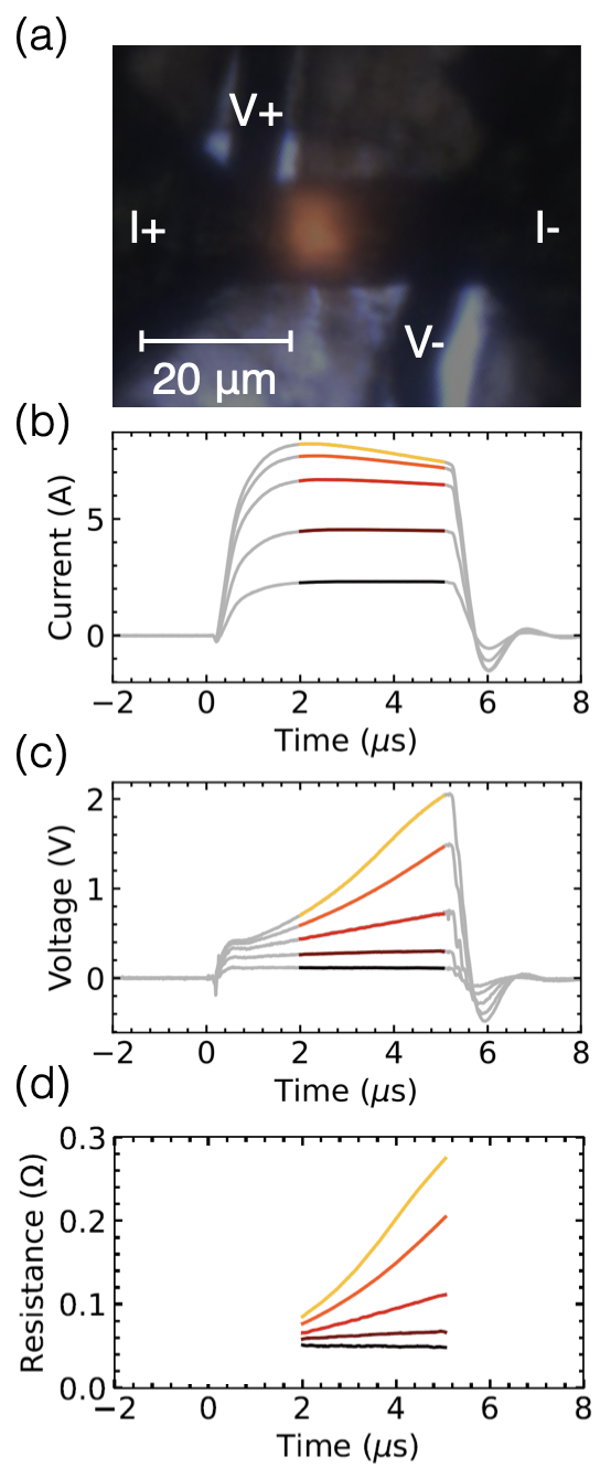
We demonstrate the utility of the pulse amplifier by using it to heat a sample of iron compressed statically to 77 GPa at room temperature. The iron sample is shaped into a four point probe geometry and compressed between layers of KCl insulation in the sample chamber of a diamond anvil cell. The sample preparation method is described in Ref. Geballe et al., 2023a.
We drive 5 s pulses of current through the sample. At pulse amplitudes A, the sample visibly heats to K, as evidenced by the orange glow in Fig. 5a, and by spectroradiometry temperature measurements described in Ref. Geballe et al., 2023b. To generate clear photos of the glow, we accumulate light from 500 heating pulses at a 1000 Hz repetition rate. A composite image of the hot sample and the sample photographed in white light shows that the sample glows orange in part of the region between voltage probes (Fig. 5a).
Examples of pulsed heating are shown in Figs 5b-d. At low current amplitude, the resistance is steady. At higher current amplitudes, the resistance increases more than 3-fold during the pulse as the sample heats to 1000s of K.
V Discussion
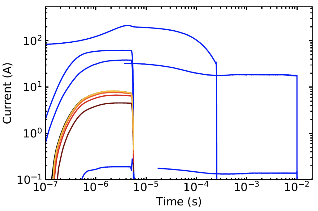
To summarize the wide range of pulses described above, we overlay many pulses in a log-log plot (Fig. 6).
To give ideas of how the pulse amplifier can be used, we describe pulses in relationship to a “prototypical pulse” for diamond cell experiments, which we define as the pulse plotted in yellow in Fig. 6. It is a 5 s pulse that peaks at A and causes the 77 GPa iron sample glow orange. The pulse amplitude can be decreased 40-fold to 0.2 A, a change that can be useful to avoid heating a sample while measuring its resistance. The pulse amplitude can be increased 7-fold to 60 A, or lengthened 200-fold to 10 ms, changes which are crucial for heating thicker or wider samples.
If a decaying pulse shape is acceptable, the prototypical 8 A pulse can be increased 25-fold to 200 A. This pulse is useful to melt relatively-thick samples at low pressure. For example, we used a pulse with A and 100s duration to melt an ambient pressure iridium sample.Geballe et al. (2023b)
Shorter duration pulses are possible by triggering the switch with TTL signals that are shorter than 5 s. As duration decreases, several issues arise. First, at s pulse duration, the plot of current-versus-time is rounded, not square, because the current rise and fall begin to overlap, at least for the m dummy sample. At 1 s pulse duration, the error in resistance measurement becomes huge (%). The voltage probes measure spurious signals during the rise and fall pulse, likely caused by inductance of the sample and current-carrying electrodes Kaschnitz, Pottlacher, and Jäger (1992). To correct for the inductance spikes, the method proposed in Ref. Kaschnitz, Pottlacher, and Jäger, 1992 could be useful. For trigger durations shorter than 1 s, the pulse amplifier fails to turn on completely, because the rise time and fall time of the drive circuitry is too slow. We attempted to decrease the rise and fall times substantially by decreasing and/or by 2-fold and 5-fold, but with no success. The rise time remained ns. In addition, the rising edge begins to oscillate at low . The ns lower limit for the rise time is surprising, because the Behlke switch has a nominal rise time of ns. Albeit, the testing reported on the manufacturer’s specification sheet is at much higher current and voltage than we use – a minimum of 25 A and 840 V.
VI Conclusions
A broadband pulse amplifier has been built and characterized. It can heat metals in diamond anvil cells up to at least 77 GPa and 2000 K. If combined with well-prepared samples, heating to 1000s of K may be possible at several megabars of pressure. The pulse amplifier delivers 0.2 to 200 A with pulse durations in the range 5 s - 10 ms. When coupled with passive current and voltage probes, the accuracy of the typical four point probe resistance measurement is better than 5%. The new pulse amplifier provides a more reliable and more versatile substitute for the amplifier used previously for pulsed Joule heating experiments up to megabar pressures.Geballe et al. (2021)
Acknowledgements.
This material is based upon work supported by the National Science Foundation under Grant No. 2125954. We thank Seth Wagner for machining parts. We thank Maddury Somayazulu for fruitful discussions.Data Availability Statement
The data that support the findings of this study are available from the corresponding author upon reasonable request.
| Label | Specifications | Brand and part number | |
|---|---|---|---|
| Oscilloscope | 200 MHz | 4 channels | Picoscope 5444D |
| Pulse Generator | 50 MHz | TTL | BNC 525 |
| HV supply (option 1) | 1250 V | 20 mA | SRS PS310 |
| HV supply (option 2) | 60 V | 18 A | XANTREX XHR 60-18 |
| HV Switch | 250 A | 8.4 kV | Behlke HTS-81-25-B |
| PP | 20 MHz | 5000 A | Pearson 411 |
| DC supply | 30 V | 5 A | Madell TPR3003 |
| 10x Probe | 400 MHz | 4 meters | Probemaster 6143-4 |
| 70 F | 500 V | TDK B32758G2706K000 | |
| 50 nF | 500 V | ||
| 3 | 50 W | Ohmite 850F3R0E | |
| 1 | 10 W | Ohmite 810F1R0E | |
| 250 k | 50 W | Ohmite L50J250KE | |
| (dummy) | 0.1 | 5W | Ohmite WHER10FET |
| 10 F | 25 V | Nichicon UPS1E100MDD | |
| 47 | 1/4 W | Ohmite OD470JE | |
| 1 | 1/2 W |
References
- Weir et al. (2012) S. T. Weir, M. J. Lipp, S. Falabella, G. Samudrala, and Y. K. Vohra, Journal of Applied Physics 111, 123529-123529-5 (2012).
- Sinmyo, Hirose, and Ohishi (2019) R. Sinmyo, K. Hirose, and Y. Ohishi, Earth Planet. Sci. Lett. 510, 45 (2019).
- Parisiades (2021) P. Parisiades, Crystals 11 (2021), 10.3390/cryst11040416.
- Alabdulkarim et al. (2023) M. E. Alabdulkarim, W. D. Maxwell, V. Thapliyal, and J. L. Maxwell, Journal of Manufacturing and Materials Processing 7 (2023), 10.3390/jmmp7020057.
- Yagi et al. (2011) T. Yagi, K. Ohta, K. Kobayashi, N. Taketoshi, K. Hirose, and T. Baba, Measurement Science and Technology 22, 024011 (2011).
- Konôpková et al. (2016) Z. Konôpková, R. S. McWilliams, N. Gómez-Pérez, and A. F. Goncharov, Nature 534, 99 (2016).
- Zaghoo, Salamat, and Silvera (2016) M. Zaghoo, A. Salamat, and I. F. Silvera, Phys. Rev. B 93, 155128 (2016).
- Geballe and Jeanloz (2012) Z. M. Geballe and R. Jeanloz, J. Appl. Phys. 111, 123518-123518-15 (2012).
- Cagran and Pottlacher (2008) C. Cagran and G. Pottlacher, in Handbook of Thermal Analysis and Calorimetry - Recent Advances, Techniques, and Applications, Vol. 5, edited by M. E. Brown and P. K. Gallagher (Elsevier, 2008) 5th ed., Chap. 9, pp. 299–320.
- Cezairliyan and McClure (1987) A. Cezairliyan and J. L. McClure, Int. J. Thermophys. 8, 577 (1987).
- Kondratyev and Rakhel (2019) A. M. Kondratyev and A. D. Rakhel, Phys. Rev. Lett. 122, 175702 (2019).
- Gallob, Jäger, and Pottlacher (1986) R. Gallob, H. Jäger, and G. Pottlacher, Int. J. Thermophys. 7, 139 (1986).
- Henry et al. (1972) K. W. Henry, D. R. Stephens, D. J. Steinberg, and E. B. Royce, Review of Scientific Instruments 43, 1777 (1972).
- Cook (2000) E. Cook, in Linac 2000, edited by A. W. Chao (2000) p. 663, arXiv:physics/0008189 [physics.acc-ph] .
- Geballe et al. (2021) Z. M. Geballe, N. Holtgrewe, A. Karandikar, E. Greenberg, V. B. Prakapenka, and A. F. Goncharov, Phys. Rev. Materials 5, 033803 (2021).
- Geballe et al. (2023a) Z. M. Geballe, S. M. Vitale, J. Yang, F. Miozzi, V. V. Dobrosavljevic, and M. J. Walter, “A diamond anvil microassembly for joule heating and electrical measurements up to 150 gpa and 4000 k,” (2023a), arXiv:2310.18176 [physics.app-ph] .
- Geballe et al. (2023b) Z. M. Geballe, F. Miozzi, C. F. Anto, J. Rojas, J. Yang, and M. J. Walter, “Spectroradiometry with sub-microsecond time resolution using multianode photomultiplier tube assemblies,” (2023b), arXiv:2310.16660 [physics.ins-det] .
- Kaschnitz, Pottlacher, and Jäger (1992) E. Kaschnitz, G. Pottlacher, and H. Jäger, International Journal of Thermophysics 13, 699 (1992).