Performance of AC-LGAD strip sensor designed for the DarkSHINE experiment
Abstract
AC-coupled Low Gain Avalanche Detector (AC-LGAD) is a new precise detector technology developed in recent years. Based on the standard Low Gain Avalanche Detector (LGAD) technology, AC-LGAD sensors can provide excellent timing performance and spatial resolution. This paper presents the design and performance of several prototype AC-LGAD strip sensors for the DarkSHINE tracking system, as well as the electrical characteristics and spatial resolution of the prototype sensors from two batches of wafers with different dose.The range of spatial resolutions of 6.5 8.2 and 8.8 12.3 are achieved by the AC-LGAD sensors with 100 pitch size.
1 Introduction
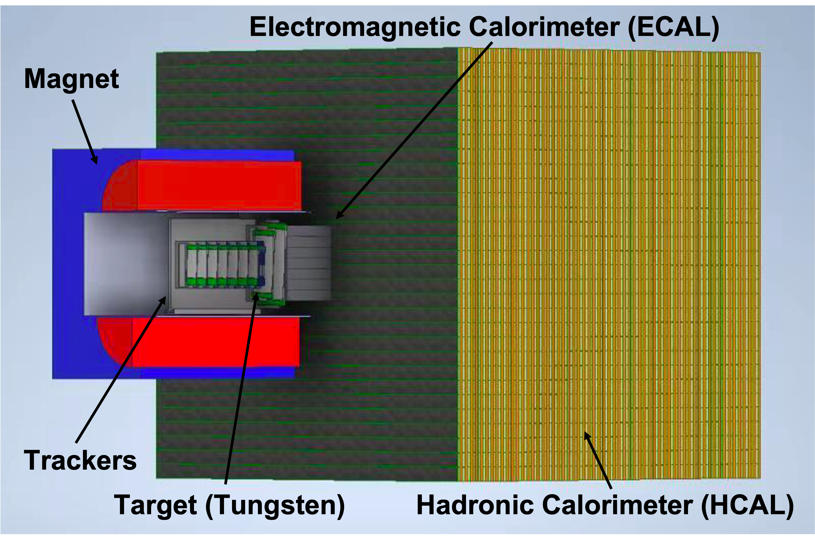
DarkSHINE experiment[1] is a newly proposed electron-on-fixed-target experiment searching for dark photon produced via electron and nucleon interaction. The dark photon then decays to a pair of dark matter candidates, which is called invisible decay[2]. Dark matter pairs escape detection as missing momentum and missing energy, also resulting in lower momentum and larger recoil angle of the recoil electron. The missing momentum signature is used to identify signal from various Standard Model background processes. Therefore, reconstruction of position and momentum of the incident and recoil electrons is crucial for this experiment.
Figure 1-(a) shows the sub-detector systems of DarkSHINE experiment. A tracking system is placed in a downward magnetic field of around 1.5 T which is provided by a superconducting magnet system. The magnetic filed direction is defined as the -direction and the electron beam direction as the -direction, hence the electron will be deflected in the -direction perpendicular to the magnetic field. As shown in Figure 1-(b), the DarkSHINE tracking system consists of seven layers of tagging modules and six layers of recoil modules, while a tungsten target with decay length is placed in between. Each layer of tracking module consists of two silicon sensors with length of at least 20 mm, placed at a small angle (100 mrad). The sensors are expected to be as thin as possible, in order to avoid multi-track events caused by the interaction between charged particles and the nucleus of the detector material. The designed position (angle) resolution of the tracking system is better than 10 (0.1%) at the direction of the electron deflection. To achieve that, several small prototype sensors are designed with technology of AC-coupled Low-Gain Avalanche Detectors (AC-LGADs, also called Resistive Silicon Detectors).
The Low-Gain Avalanche Detector (LGAD)[3] has been developed in recent years, with a novel precise detector technology initially proposed and designed for the precise timing measurements of the High Granularity Timing Detector of ATLAS[4] and the Endcap Timing Layer of CMS[5] for the High-Luminosity Large Hadron Collider. Figure 2-(a) shows a sketch of a LGAD sensor. The LGAD sensors are fabricated on high-resistivity -type substrates with thickness of about 50 . Based on traditional -in- silicon sensor, the LGAD sensor has an additional highly-doped region (namely “gain layer”) under the parallel - junction. When a bias voltage is applied across the sensor, this layer will be depleted and create a strong local electric field, therefore introducing an internal gain.
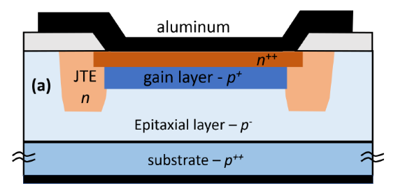
In order to achieve better spatial resolution while maintaining similar gain and fast timing performance, the AC-coupled LGAD (AC-LGAD) technology has been brought up where the signal are capacitively induced and shared among the metal AC-pads. Figure 2-(b) shows a sketch of an AC-coupled LGAD sensor. The AC-pads of the sensor for signal readout are placed on a thin dielectric layer which is grown over the layer of the sensor. The AC-LGADs has much less doped layer comparing to the layer in the standard LGADs. It results in an increased inter-pad resistance[6]. A highly-doped implant is still preserved at the edge of the active area of the sensor, in order to have DC-connection for electron current draining. The AC-LGAD design can easily adapt to any detector geometry since the segmentation can be achieved by the AC-pads of any shape.
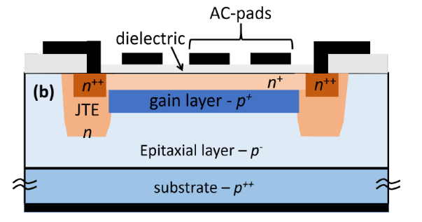
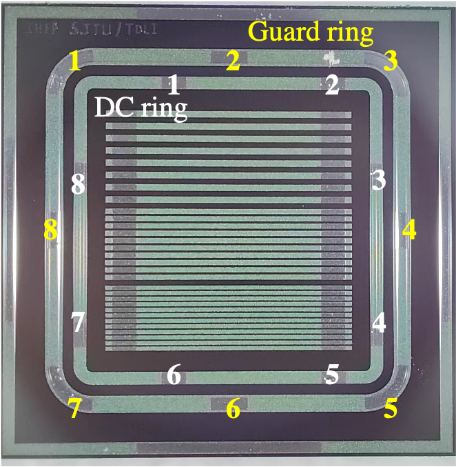
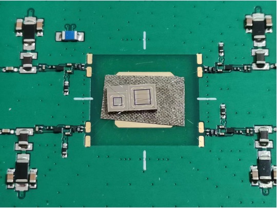
Two types of strip sensors with pitch (strip) size of 100 (50) , 60 (40) , and 45 (30) are designed for the DarkSHINE experiment. Two batches of wafers of AC-LAGD strip sensor prototypes have been produced by the Institute of Microelectronics, which are based on the AC-LAGD technology designed by the Institute of High Energy Physics (IHEP), CAS. They are named as wafer-11 and wafer-12 sensor in the following context. The doses of these two wafers are 0.01 P and 10 P, where P is the unit of phosphorus dose defined for the AC-LGADs[7]. Smaller dose leads to higher resistance of the sensor and therefore smaller leakage current. Thus it is expected to have better performance on the position reconstruction and spatial resolution. Figure 3 shows the design and a picture of a fabricated AC-LGAD strip sensor prototype (size of ). There are three rings which are (from outside to inside) the outer ring, the Guard Ring (GR), and the DC ring. The sensors have a 50 epitaxial layer and a 725 substrate.
2 AC-LGAD sensor I-V and C-V performance test
2.1 Measurement setup
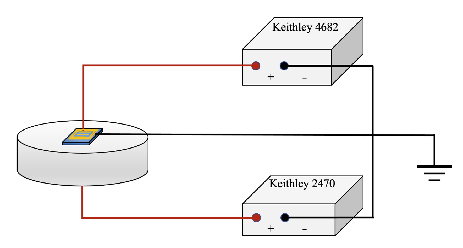
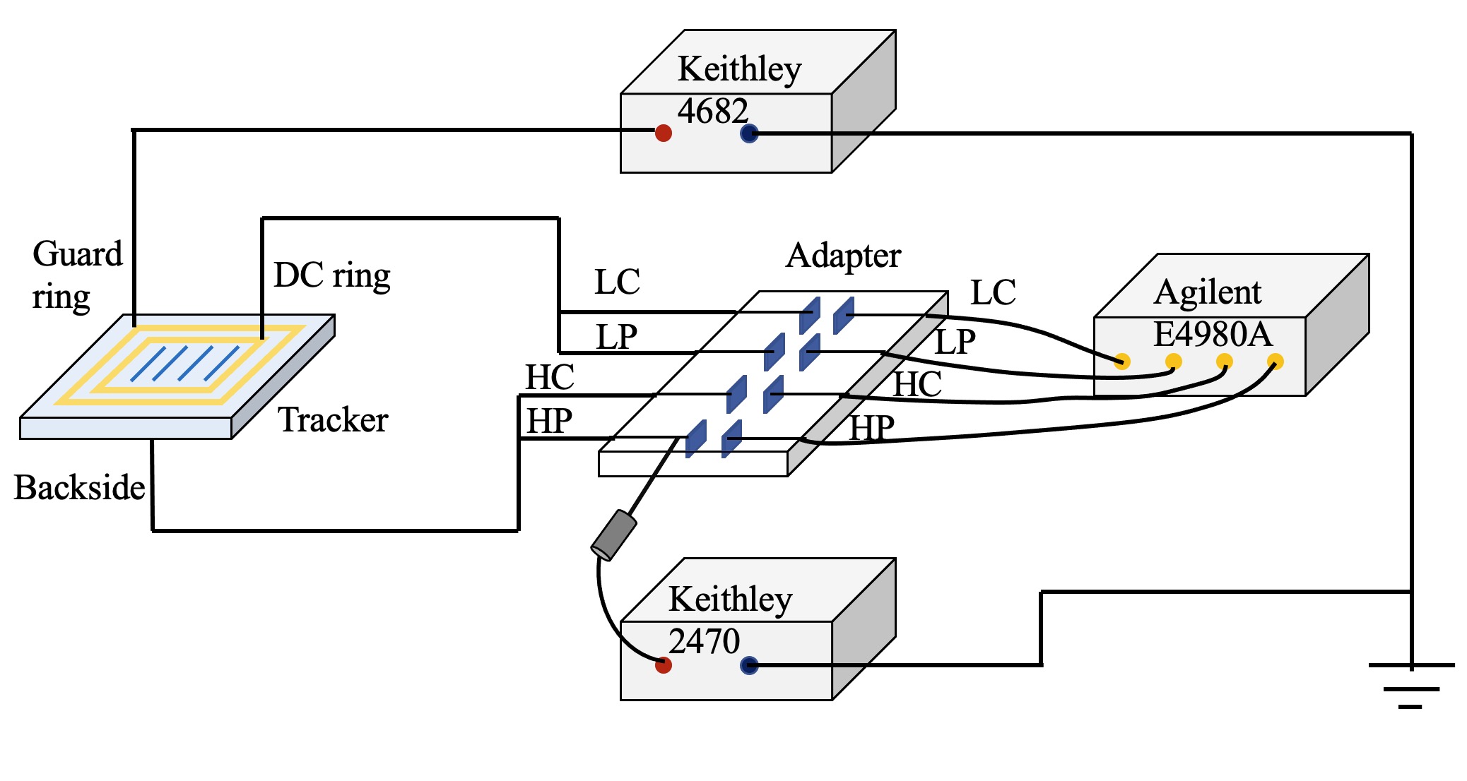
The sensors I-V and C-V tests are carried out in the tracking lab at Shanghai Jiao Tong University. The wiring setups for I-V and C-V measurements are illustrated in Figure 4. A four-channel (LC, LP, HC, HP) HV adapter is connected in parallel between the sensor and the LCR meter to limit the voltage within a safe range. In C-V measurement, the LCR meter works on the “Cp-Rp” mode at a frequency of 10kHz according to the recommendation of RD50 [8]. The measurements are carried out in darkness to avoid additional light current.
2.2 Current-voltage measurement
The measured I-V performance is shown in Figure 5. The breakdown voltage () of wafer-11 (wafer-12) sensor, which is defined as the reverse bias voltage applied when the leakage current reaches 500 nA, is around 380 V (185 V) at room temperature ( 25∘C). Wafer-11 has higher than wafer-12 due to higher resistance. Figure 5-(b) shows the I-V curves measured at different temperatures: 5∘C, 15∘C, 25∘C and 30∘C. As temperature increases, the current and also increases due to thermal motion of the electron-hole pairs. This result suggests that working voltage of the wafer-11 (wafer-12) sensors should be set below 350 V (150 V).


Figure 6 shows I-V uniformity dependency. The measurement is carried out at room temperature. The bias voltage is scanned in steps of 5 V, whilst it is 1 V scanning step close to breakdown voltage. As shown in Figure 6-(a), the leakage current shifts a little according to the position of the sensor on the wafer due to the non-uniformity of doping. As shown in Figure 6-(b), the I-V curves are measured with two probe needles on different position of the GR and the DC ring, as marked in Figure 3. The obtained I-V curves are all the same which indicates that the doping within the active region of the sensor can be considered as being uniform.

2.3 Capacitance-voltage measurement
The capacitance-voltage (C-V) curves indicate performance of multiplication layer inside the AC-LGAD sensors. The AC-LGAD sensors are tested at room temperature, and bias voltage is scanned in steps of 1 V.
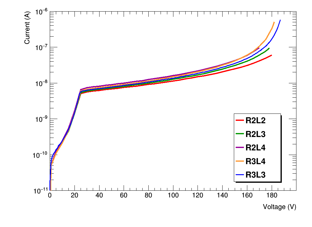
Figure 7-(a) shows the measured C-V curves of one wafer-11 sensor and three wafer-12 sensors, while figure 7-(b) shows the corresponding -V curves. No obvious difference in the C-V curves has seen for sensors from different position on wafer-12. It shows that the doping uniformity among wafer has negligible effect on the junction capacitance. There are two plateaus on the curves. The curves start rising after the first plateau at the voltage of around 20 V (24 V) for wafer-11 (wafer-12) sensors, which voltages indicate that their gain layers are fully depleted. After gain layer depletion, the curves rising part of wafer-11 and wafer-12 sensors are similar, since they have the same bulk resistivity. The wafer-11 and wafer-12 sensors both saturate and enter a second plateau at approximately 40 V voltage value.


3 Position reconstruction and spatial resolution test
3.1 Measurement setup
To investigate spatial resolution of the AC-LGAD sensor, four adjacent strips on the sensor are tested on a transient current technique (TCT) platform which are bonded to a 4-channel readout PCB board. As shown in Figure 8-(a), a 4-channel readout PCB board is developed and is produced at IHEP with reference to the single-channel readout board designed by University of California Sanata Cruz[9]. A bias voltage is supplied through the back of sensors while its guard ring is grounded. The working voltage is set to V ( V) for wafer-11 (wafer-12) sensor according to its I-V curve measured in Section 2.2. Only 100 pitch design is tested in this paper.
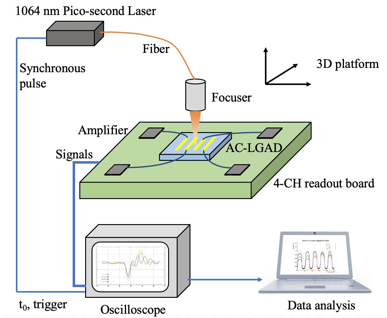
The setup of TCT platform is illustrated in Figure 8-(b). The laser wavelength is 1064 nm. The laser spot, with size of about 6 , can be moved along either or direction which is controlled by a 3-dimensional translation platform with accuracy around 1 . In order to simulate single photon event, an attenuator is placed above the sensor. The signal is triggered by a synchronous pulse from laser with a potential trigger time shift of around 15 ps. After amplification the signal pulses readout from four wire bonded strips are recorded by digital oscilloscope. It has a sampling width of 20 Gs/s and bandwidth of 1 GHz.
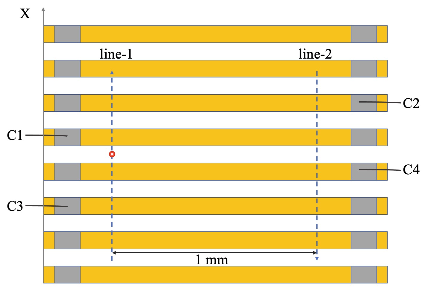
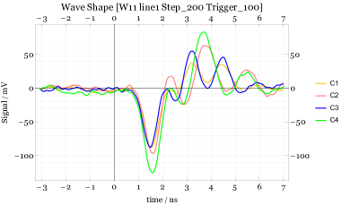
The laser spot is moved with 2 step size along the plus and minus directions perpendicular to the strips, which is illustrated as line-1 and line-2 in Figure 9-(a). The coordinate is fixed during the measurement. During a data-taking period the oscilloscope is triggered by the laser around 1300 times. Four signal pulses are recorded in each triggered event which is shown as the deepest peaks in Figure 9-(b). The signal waveforms have typically 1 ns width. The dependence of peak amplitudes comes from different distances between the readout strips and the laser spot. The peaks with opposite polarity come from electron diffusion within layer towards the edge of the sensor[6].
3.2 Position reconstruction and spatial resolution
A simplified linear model[10] is used to reconstruct the position of signal (i.e. the laser spot centre). This linear model assumes that signal on each pad decreases linearly with its distance from the point of particle incidence. For strip sensors, the position information recorded by four strip sensors has only one dimension. As shown in figure 9, signal fraction is defined as ratio of the lowest peak of each channel to the lowest peak of all channels. It can be assumed that the signal fraction on each strip varies linearly with the distance from the impact point. The relationship between the impact position and the signal fraction of each strip can be expressed by
where is the impact position, is the signal fraction of each channel, is the signal fraction of each channel at , and is the change rate of the signal fraction of each channel with the impact position.
Figure 10-(a) shows the maximum amplitudes of the four channels, which is averaged over all triggers in each step. When laser spot is blocked by the metal strips, the collected charge or signal amplitude reduces to zero. We set at centre of the gap between C1 and C4. This is derived by finding the edges of the metal strip after deriving the signal distribution for each channel.
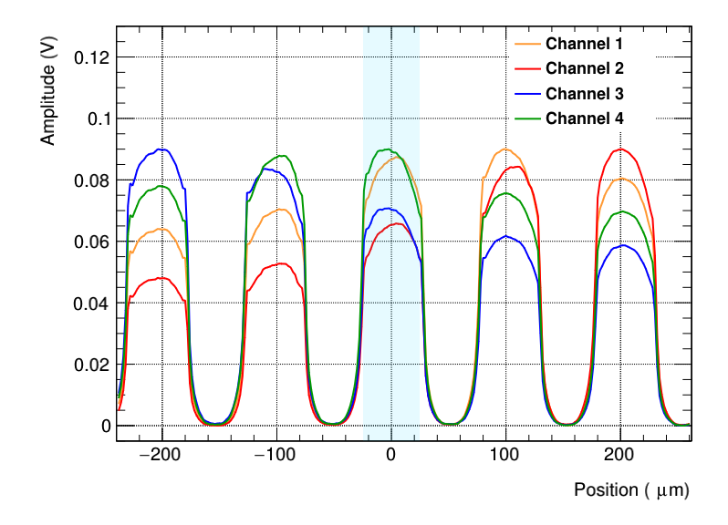
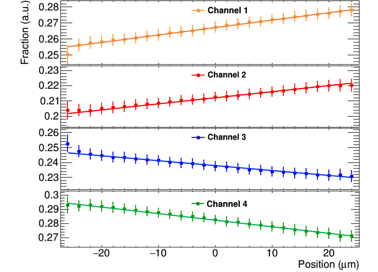
Figure 10-(b) shows the fraction of the maximum amplitude of each readout channel as a function of , computed by
where is the maximum amplitude of each channel at given . A linear function is then used to fit the amplitude fraction of each channel. Therefore, four values can be solved from the fit function for any given event with measured amplitude fraction , and the average among is taken as the reconstructed laser spot position.
Figure 11-(a) shows a distribution of the reconstructed coordinates for a known test position at . From a Gaussian fit to this distribution, its mean value -0.88 is taken as the reconstructed , and its sigma value 9.63 is considered as the spatial resolution.

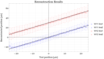
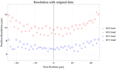
Figure 11-(b) shows two sets of reconstructed positions from wafer-11 and wafer-12 and a comparison with spot positions. The dashed lines indicate spot positions while the dots are reconstructed positions. They are in good agreement. Figure 12-(a) shows the corresponding spatial resolution as a function of , which varies from 6.5 to 8.2 for wafer-11 and from 8.8 to 12.3 for wafer-12 respectively. Better resolution of wafer-11 sensor than wafer-12 is due to the fact that dose (0.01 P) of wafer-11 is much smaller than wafer-12 (10 P). The spatial resolution is slightly worse in the edge of gaps as shown in figure 12-(b). It is due to the fact that signal fraction is less stable when laser spot closing to metal strips. Similar effect also leads to a small overall discrepancy between the line-1 and line-2 measurements.
4 Summary
This paper presents the performance of two batches of prototype AC-LGAD sensors with pitch size of 100 designed for the DarkSHINE experiment. The range of spatial resolutions are 6.5 8.2 and 8.8 12.3 for wafer-11 and wafer-12 sensors. The typical sensor response time is about 1 ns. The wafer-11 sensor delivers better spatial resolution because of smaller dose. Both wafer-11 and wafer-12 sensors satisfy the requirement of the DarkSHINE tracking system.
This work has been supported by a grant from the National Natural Science Foundation of China (Grant NO.12150006).
References
- [1] J. Chen, et al, Prospective study of light dark matter search with a newly proposed DarkSHINE experiment, Sci. China Phys. Mech. Astron. 66 (2023) 211062.
- [2] M. Fabbrichesi, E. Gabrielli, and G. Lanfranchi, The dark photon. arXiv: 2005.01515
- [3] H.F.W. Sadrozinski et al., Ultra-fast silicon detectors, Nucl. Instrum. Meth. A 730 (2013) 226.
- [4] ATLAS collaboration, Technical Proposal: A High-Granularity Timing Detector for the ATLAS Phase-II Upgrade. CERN-LHCC-2018-023.
- [5] CMS collaboration, Technical proposal for a MIP timing detector in the CMS experiment phase 2 upgrade, CERN-LHCC-2017-027.
- [6] G. Giacomini, W. Chen, G. D’Amen and A. Tricoli, Fabrication and performance of AC-coupled LGADs, JINST 14 (2019) P09004.
- [7] M. Li, et al., The performance of large-pitch AC-LGAD with different N+ dose, (2022) arxiv:2212.03754.
- [8] A. Chilingarov, RD50-Recommendations for performing measurements. Part I: IV and CV measurements in Si diodes.
- [9] N. Cartiglia, et al., Beam test results of a 16 ps timing system based on ultra-fast silicon detectors, Nucl. Instrum. Methods Phys. Res. A 850 (2017) 83-88.
- [10] M.Tornago, R. Arcidiacono et al., Resistive AC-Coupled Silicon Detectors: Nucl. Instrum. Methods Phys. Res. A 1003(2021) 165319.