Tuning the supercurrent distribution in parallel ballistic graphene Josephson junctions
Abstract
We report on a ballistic and fully tunable Josephson junction system consisting of two parallel ribbons of graphene in contact with superconducting MoRe. By electrostatic gating of the two individual graphene ribbons we gain control over the real space distribution of the superconducting current density, which can be continuously tuned between both ribbons. We extract the respective gate dependent spatial distributions of the real space current density by employing Fourier- and Hilbert transformations of the magnetic field induced modulation of the critical current. This approach is fast and does not rely on a symmetric current profile. It is therefore a universally applicable tool, potentially useful for carefully adjusting Josephson junctions.
Josephson junctionsJosephson (1962), which consist of two superconductors connected by a normal conducting material or an insulator, have been investigated for a long time, since they can be used for infrared detectorsWalsh et al. (2017), ultrafast logic circuitsBunyk, Likharev, and Zinoviev (2001) or sensitive magnetic flux and voltage measurementsGrundmann (2005). Additionally, Josephson junctions are a powerful tool for exploring the properties of superconductors by connecting the supercurrent to the phase of the macroscopic wave functionGross, Marx, and Deppe (2016). In the last decade, Josephson junctions have also been employed as building blocks for superconducting quantum computingHuang et al. (2020); Kjaergaard et al. (2020); Blais et al. (2021). Substituting the normal conductor or insulator with graphene as the weak link, leads to highly tunable Josephson junctions with transparent interfaces due to the absence of a Schottky barrierCalado et al. (2015). In the past, graphene-based Josephson junctionsKe et al. (2016); Borzenets et al. (2016); Heersche et al. (2007); Du, Skachko, and Andrei (2008); Ojeda-Aristizabal et al. (2009); Borzenets et al. (2011); Komatsu et al. (2012); Mizuno, Nielsen, and Du (2013); Choi et al. (2013); Li et al. (2018a) have been investigated by tunneling spectroscopyBretheau et al. (2017); Wang et al. (2018) and have been used to study crossed Andreev reflectionPark et al. (2019) and superconductivity in the quantum Hall regimeRickhaus et al. (2012); Draelos et al. (2018); Zhao et al. (2020); Gül et al. (2022). Besides the magnitude of the supercurrent carried over the Josephson junction, the spatial current distribution has been analyzed in the case of edge currents in grapheneZhu et al. (2017); Allen et al. (2016, 2017) and for studying topological Josephson junctionsYing et al. (2020). Furthermore, the control and determination of the current density is important for the operation of protected Josephson rhombus chains Bell et al. (2014) or protected superconducting qubits based on tunable Josephson interferometer arraysSchrade, Marcus, and Gyenis (2022). Here, the pairwise balance of the Josephson junctions protects the qubit against detuning or noise. However, the real space current density is not directly accessible in electrical transport measurements.
To obtain the real space current density of two coupled Josephson junctions, an out-of-plane magnetic field has to be applied to the junction, which leads to a modulation of the critical current. This can be expressed as the magnitude of a Fourier transform of the real space current density, which, thus, can be reconstructed from the modulation of the critical current by an inverse Fourier transformDynes and Fulton (1971). Even though this method has been recently applied to a gated epitaxial Al-InAs Josephson junctionElfeky et al. (2021), highly non-symmetric cases have not been studied so far. In this work, we study a fully tunable graphene double Josephson junction formed by two parallel ribbons with superconducting molybdenum-rhenium (MoRe) contacts. By using both top and back gates, we can independently tune the supercurrent distribution between the two ribbons. We present results based on a reconstruction of the supercurrent from the magnetic field dependent critical current using a combination of Fourier and Hilbert transformations, which allows to extract the asymmetric supercurrent distribution.
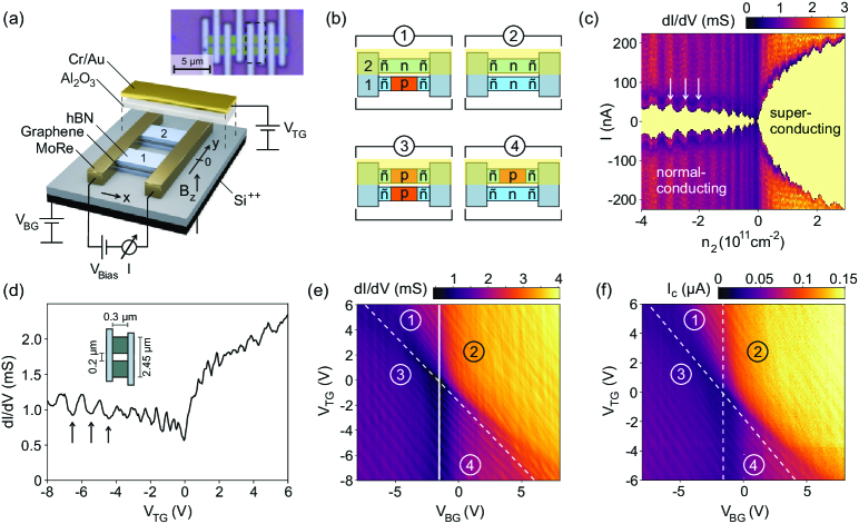
A schematic and an optical micrograph of our device is shown in Fig. 1a. It consists of graphene grown by chemical vapor deposition (CVD), which is encapsulated in hexagonal boron nitride (hBN) crystals by dry transfer van der Waals stacking.Wang et al. (2013); Banszerus et al. (2015, 2016) The stack is etched into two parallel ribbons by CF4/O2 reactive ion etching (RIE) through a polymethyl methacrylate (PMMA) resist mask, which has been patterned by standard electron beam lithography to a width of with a separation of between the two ribbons. The graphene is electrically contacted to superconducting MoRe electrodes, fabricated by sputter deposition defining the junction length of . Separated by 300 nm SiO2 gate dielectric, the device is placed on a highly doped silicon substrate acting as a back gate. Additionally, a gold top gate is deposited onto one of the graphene ribbons, while the whole device is protected by an insulating layer of Al2O3 grown by atomic layer deposition (ALD). This allows us to tune the charge carrier density of the two graphene ribbons independently since one of them is only affected by the back gate (BG) leading to a charge carrier density of while the other ribbon is tuned by the combination of both top gate (TG) and back gate voltages , where and are the respective gate lever arms, which are proportional to the capacitive coupling of the respective gate to the graphene. The gate settings and account for a constant shift of the charge neutrality point and the gate lever arms are estimated to be and . With this individual gate tuning, the device can be tuned into four regimes defined by the polarities of the two ribbons, see Fig. 1b: p|n (1), n|n (2), p|p (3) and n|p (4). All measurements were performed in a He3/He4 dilution refrigerator with a base temperature of around 10 mK. A constant parasitic resistance of arises from the wiring and the filters.
In Fig. 1c we show the differential conductance of the device as function of the current and charge carrier density , which is tuned by the top gate voltage while the back gate voltage is set to the charge neutrality point (). A superconducting regime (yellow color) is present symmetric around for both electron () and hole () doping and can be distinguished from the normal conducting regime at larger current values. The current at which the transition between these two regimes occurs defines the critical current . Here it is important to note that no influence of the current sweep direction on the critical current has been observed.
Oscillations of the differential conductance and the critical current that are observed in the p-doped region () can be attributed to Fabry-Pérot (FP) interferenceRickhaus et al. (2013); Ben Shalom et al. (2016). They originate from the -p- graphene cavity in the double gated ribbon, which is formed by the MoRe yielding a highly local doping in the graphene nearby the contacts (see Fig. 1b). The critical current becomes largest for n-doping () since there is no p- junction, which increases the resistance. Since the carrier density is only weakly tuned in the outer graphene parts next to the MoRe contacts, there is no cavity formed, as seen by the suppression of FP oscillations in this regime. The FP oscillations are further explored in Fig. 1d, where we plot the normal state conductance, measured at a bias voltage of to keep the junction in the normal state regime, at fixed back gate voltage and varying top gate voltage. Analyzing the FP oscillations (see Supplementary Material for details) for both ribbons results in an extracted cavity length of and which fits well to the lithographic length of the channel (see inset in Fig. 1d for sample dimensions), in agreement with ballistic and phase coherent transport. In Fig. 1e, we show the normal state conductance of the device as function of top- and back gate voltages. The four possible doping configurations sketched in Fig. 1b can be identified (see labels in Figs. 1e,f). The top gate voltage only changes the charge carrier density of the respective graphene ribbon underneath, while the back gate voltage influences both ribbons. Configuration (1) refers to the situation of a -p- junction in one ribbon, while the other (underneath the top gate) is completely n-doped. The complementary configuration, denoted as (4), has the -p- junction underneath the top gate. Configuration (3) refers to the case of both ribbons tuned to a -p- junction. Here, a combination of the FP oscillations by the two gates can be seen. Finally, configuration (2) describes the case of unipolar n-type doping for both ribbons and thus the absence of any p- junctions, which results in an enhanced conductance. Reducing the bias voltage and thus entering the superconducting state enables us to extract the critical current . The critical current is plotted as function of top- and back gate voltages in Fig. 1f. The map resembles most features of the conductance map in Fig. 1e. Combining the critical current and the normal state resistance gives an product between and , comparable to results in the literatureLi et al. (2018b).
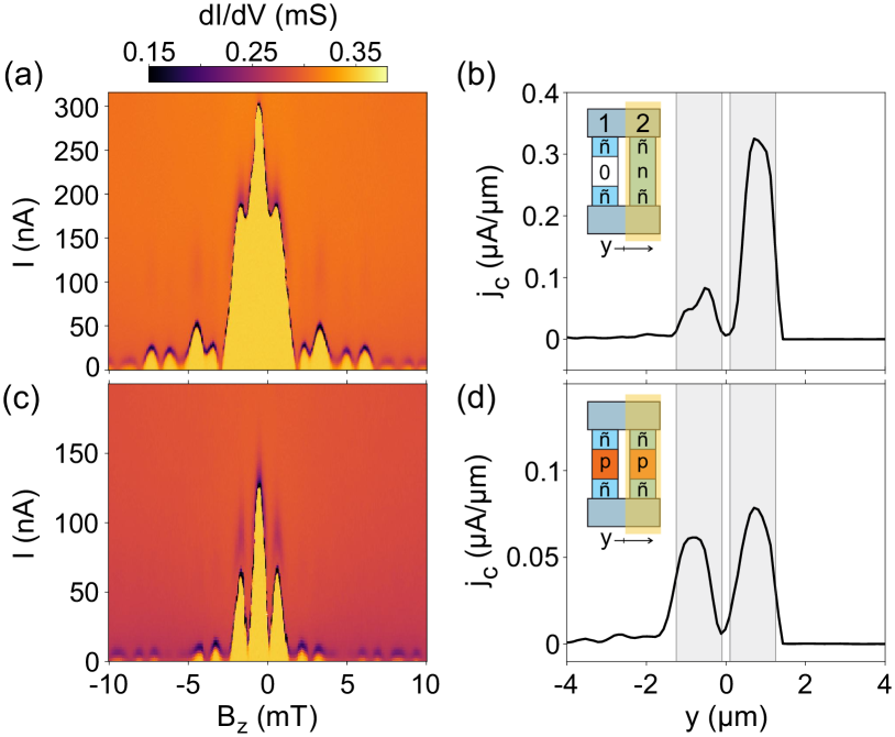
Next we focus on the magnetic field dependence of the critical current, which will allow to reconstruct its spatial distribution. We measure the differential conductance while varying both the current and the out-of-plane magnetic field . The magnetic field induces a phase difference between the two bulk superconductors, leading to a modulation of the critical current Rowell (1963) as shown in Fig. 2a for the case of one graphene ribbon being conductive (-n-) while the other is tuned near the charge neutrality point (-0-) (see inset of Fig. 2b). To gain information on the real space superconducting current density distribution, , we perform an inverse Fourier transformation (FT) of the extracted combined with a Hilbert transformation to reconstruct the phase of the signal as introduced by Dynes and Fulton Dynes and Fulton (1971), see Supplementary Material for details. Note that the reconstructed data leaves the freedom of an arbitrary offset in the position together with the sign of (which corresponds to mirroring around ). We correct the reconstructed data such that position correspond to the center of the two graphene ribbons and flip the -axis such that the major peak corresponds to the ribbon with the larger conductance. Here, the junction tuned by the back gate only, is located at negative position () whereas the top gated junction is located at positive position (). The extracted current density distribution in Fig. 2b of the measurement shown in Fig. 2a visualizes the asymmetric supercurrent distribution in this configuration with the largest critical currents along the (-n-) ribbon at . Changing the gate voltages to the symmetric configuration (see configuration (3) in Fig. 1b), where both graphene ribbons are p-doped shows a different modulation pattern (see Fig. 2c) and the extracted supercurrent density shows indeed an even current distribution between the two ribbons (see Fig. 2d). We use the width of these current peaks to adapt the -axis of the reconstructed data to with the magnetic flux quantum and . Taking into account the length obtained by the analysis of FP oscillations of results in a London penetration depth of .
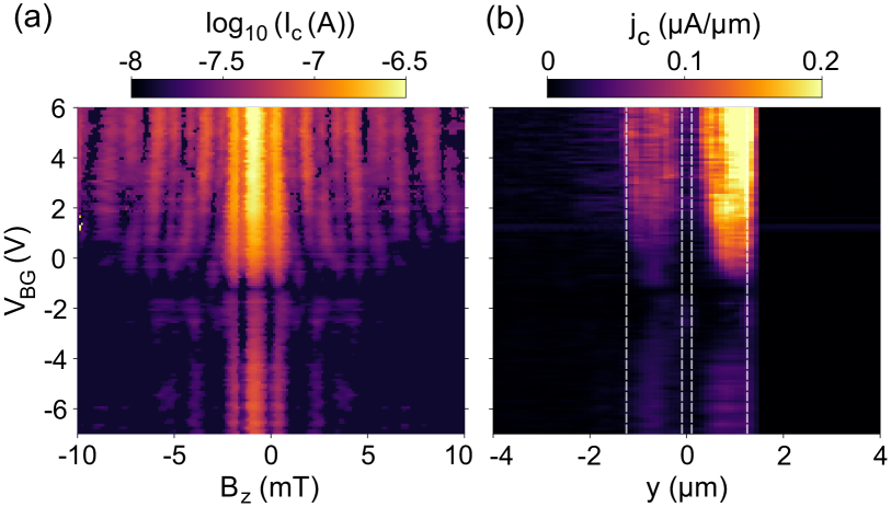
To measure the critical current directly instead of extracting it from multidimensional measurements, we used a home-built circuit which detects the peak in differential resistance when sweeping the applied current (see Supplementary Material for details). This allows an enhanced measurement speed by a factor of 60 and opens the door to measure the modulation patterns as a function of the applied gate voltages. In Fig. 3a, we show the logarithm of the critical current as function of magnetic field and . Again, the magnetic field induced modulation that depends on the applied back gate voltage is visible by the features of brighter colors. Even the modulation features of low intensity at higher magnetic fields can be seen. Strikingly, the critical current is lower for negative back gate voltages, because of the resulting -p--junction, which increases the normal resistance which is less pronounced for positive voltages. We perform the reconstruction for each line and show the gate dependent real space current distribution in Fig. 3b. The most important features are the two distinctive areas with high current densities at which correspond to the two graphene ribbons. It can be seen that the back gate indeed tunes both junctions and thus changes the current densities for the areas at and . The asymmetry is caused by the top gate influencing only ribbon 2 (see Figs. 1a,b).
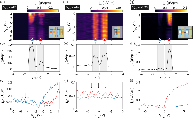
We now focus on the real space superconducting current densities for different electrostatic configurations in more detail. In the first configuration, presented in Fig. 4a, most current flows through ribbon 1 that is not covered by the top gate at . In Fig. 4a the superconducting current density is plotted as function of real space position and back gate voltage. The back gate voltage tunes the bulk of ribbon 1 from n-doping at to p-doping, resulting in a -p- configuration at while the fixed top gate voltage keeps the bulk of ribbon 2 for all values p-doped (i.e. in the -p- configuration), as shown by the inset in Fig. 4a. The map shows two vertical features of high current density that can be assigned to the supercurrents running through the two ribbons. The highest current density is present in case of n-doping () for , resulting from the higher normal conductance of the -n- ribbon. In Fig. 4b we show a line-cut along the dashed line in Fig. 4a where the asymmetry is well visible as the peak at is more pronounced. Additionally, line-traces of the current density as function of extracted at the center positions of the two ribbons (see blue and red triangles in Fig. 4a) are shown in Fig. 4c. While ribbon 1 (blue trace) shows a clear transition from reduced current density with FP oscillations at to an increasing current density for , ribbon 2 (red trace) shows FP oscillations even for positive values (see black arrows). This gives us an unambiguous way to identify the peaks in the current density as the junction with or without top gate.
A similar analysis is performed for the configuration where we fix and tune so that both graphene ribbons are p-doped (see Fig. 4d-f). Here, the gate voltage and position dependent current density (Fig. 4d) shows a rather symmetric distribution between the two ribbons visualized by the two parallel vertical strips of high current density for all measured top gate voltages. The even distribution can also be seen in the line-cut at , see Fig. 4e. Moreover, we observe an oscillatory modulation of the real space current density with respect to the gate voltage due to FP interference in the -p- cavity. This effect becomes more visible in the gate dependent line-cuts at the position of the two ribbons as indicated by the vertical arrows (see Fig. 4f). In this configuration the FP oscillation is only present for the ribbon underneath the top gate (ribbon 2), since is kept constant and thus the tuning of charge carrier density leading to the FP oscillation is asymmetric.
Finally, in Figs. 4g-i we show a third configuration where only the graphene ribbon underneath the top gate is conductive, while the other is tuned to its charge neutrality point by the back gate. Consequently, the extracted current density shows a highly asymmetric distribution among the ribbons with almost no supercurrents at , see Fig. 4g. This also becomes clear in the line-cut at (Fig. 4h), where only one significant peak at can be identified. Furthermore, the current suppression in the case of a -p- junction can be seen in Fig. 4i when comparing the current density at negative and positive gate voltage. This fits well to the observed difference in critical current for n- and p-doping (compare to Fig. 1f).
In summary, we presented a fully tunable graphene-based double Josephson junction consisting of two parallel graphene ribbons contacted by MoRe. We showed a remarkable control over these junctions and are able to individually tune the charge carrier densities of both ribbons. This allows us to continuously control the distribution of the superconducting current density in the two ribbons independently. Through ballistic transport, ensured by the dry transfer fabrication method of the device, we were able to observe FP oscillations. From these oscillations, we could determine the length of the electrostatic -p- cavity between the superconducting contacts. In order to test the tuning capabilities of the graphene Josephson junction we measured the critical current depending on magnetic field and gate voltages leading to the magnetic field induced modulation of the critical current. Most interestingly, we could map the current density distributions in real space of the individual graphene ribbons, highlighting the FP oscillations present in the individual ribbons and proving the excellent gate tunability of the junctions from an even to a fully asymmetric current distribution. This opens the door of controlling and monitoring the current densities in complex Josephson interferometer circuits potentially leading to protected superconducting qubitsSchrade, Marcus, and Gyenis (2022).
Acknowledgements.
We thank U. Wichmann for help with the measurement electronics. This project has received funding from the Deutsche Forschungsgemeinschaft (DFG, German Research Foundation) under Germany’s Excellence Strategy – Cluster of Excellence Matter and Light for Quantum Computing (ML4Q) EXC 2004/1 – 390534769, the European Union’s Horizon 2020 research and innovation programme under grant agreement No. 881603 (Graphene Flagship) and from the European Research Council (ERC) (grant agreement No.820254)), and the Helmholtz Nano Facility Albrecht, Moers, and Hermanns (2017). K.W. and T.T. acknowledge support from JSPS KAKENHI (Grant Numbers 19H05790, 20H00354 and 21H05233) and A.K.H. acknowledges support from the DFG (Hu 1808/4-1, project id 438638106).Data availability The data supporting the findings are available in a Zenodo repository under accession code https://doi.org/10.5281/zenodo.7632431.
References
- Josephson (1962) B. Josephson, Physics Letters 1, 251 (1962).
- Walsh et al. (2017) E. D. Walsh, D. K. Efetov, G.-H. Lee, M. Heuck, J. Crossno, T. A. Ohki, P. Kim, D. Englund, and K. C. Fong, Phys. Rev. Applied 8, 024022 (2017).
- Bunyk, Likharev, and Zinoviev (2001) P. Bunyk, K. Likharev, and D. Zinoviev, International Journal of High Speed Electronics and Systems 11, 257 (2001).
- Grundmann (2005) M. Grundmann, in Encyclopedia of Condensed Matter Physics, edited by F. Bassani, G. L. Liedl, and P. Wyder (Elsevier, Oxford, 2005) pp. 17–22.
- Gross, Marx, and Deppe (2016) R. Gross, A. Marx, and F. Deppe, Applied Superconductivity: Josephson Effect and Superconducting Electronics, De Gruyter Textbook Series (Walter De Gruyter Incorporated, 2016).
- Huang et al. (2020) H.-L. Huang, D. Wu, D. Fan, and X. Zhu, Science China Information Sciences 63, 180501 (2020).
- Kjaergaard et al. (2020) M. Kjaergaard, M. E. Schwartz, J. Braumüller, P. Krantz, J. I.-J. Wang, S. Gustavsson, and W. D. Oliver, Annu. Rev. Condens. Matter Phys. 11, 369 (2020).
- Blais et al. (2021) A. Blais, A. L. Grimsmo, S. M. Girvin, and A. Wallraff, Rev. Mod. Phys. 93, 025005 (2021).
- Calado et al. (2015) V. E. Calado, S. Goswami, G. Nanda, M. Diez, A. R. Akhmerov, K. Watanabe, T. Taniguchi, T. M. Klapwijk, and L. M. K. Vandersypen, Nature Nanotechnology 10, 761 (2015).
- Ke et al. (2016) C. T. Ke, I. V. Borzenets, A. W. Draelos, F. Amet, Y. Bomze, G. Jones, M. Craciun, S. Russo, M. Yamamoto, S. Tarucha, and G. Finkelstein, Nano Letters 16, 4788 (2016).
- Borzenets et al. (2016) I. V. Borzenets, F. Amet, C. T. Ke, A. W. Draelos, M. T. Wei, A. Seredinski, K. Watanabe, T. Taniguchi, Y. Bomze, M. Yamamoto, S. Tarucha, and G. Finkelstein, Phys. Rev. Lett. 117, 237002 (2016).
- Heersche et al. (2007) H. B. Heersche, P. Jarillo-Herrero, J. B. Oostinga, L. M. K. Vandersypen, and A. F. Morpurgo, Nature 446, 56 (2007).
- Du, Skachko, and Andrei (2008) X. Du, I. Skachko, and E. Y. Andrei, Phys. Rev. B 77, 184507 (2008).
- Ojeda-Aristizabal et al. (2009) C. Ojeda-Aristizabal, M. Ferrier, S. Guéron, and H. Bouchiat, Phys. Rev. B 79, 165436 (2009).
- Borzenets et al. (2011) I. V. Borzenets, U. C. Coskun, S. J. Jones, and G. Finkelstein, Phys. Rev. Lett. 107, 137005 (2011).
- Komatsu et al. (2012) K. Komatsu, C. Li, S. Autier-Laurent, H. Bouchiat, and S. Guéron, Phys. Rev. B 86, 115412 (2012).
- Mizuno, Nielsen, and Du (2013) N. Mizuno, B. Nielsen, and X. Du, Nature Communications 4, 2716 (2013).
- Choi et al. (2013) J.-H. Choi, G.-H. Lee, S. Park, D. Jeong, J.-O. Lee, H.-S. Sim, Y.-J. Doh, and H.-J. Lee, Nature Communications 4, 2525 (2013).
- Li et al. (2018a) T. Li, J. Gallop, L. Hao, and E. Romans, Superconductor Science and Technology 31, 045004 (2018a).
- Bretheau et al. (2017) L. Bretheau, J. I.-J. Wang, R. Pisoni, K. Watanabe, T. Taniguchi, and P. Jarillo-Herrero, Nature Physics 13, 756 (2017).
- Wang et al. (2018) J. I.-J. Wang, L. Bretheau, D. Rodan-Legrain, R. Pisoni, K. Watanabe, T. Taniguchi, and P. Jarillo-Herrero, Phys. Rev. B 98, 121411 (2018).
- Park et al. (2019) G.-H. Park, K. Watanabe, T. Taniguchi, G.-H. Lee, and H.-J. Lee, Nano Lett. 19, 9002 (2019).
- Rickhaus et al. (2012) P. Rickhaus, M. Weiss, L. Marot, and C. Schönenberger, Nano Lett. 12, 1942 (2012).
- Draelos et al. (2018) A. W. Draelos, M. T. Wei, A. Seredinski, C. T. Ke, Y. Mehta, R. Chamberlain, K. Watanabe, T. Taniguchi, M. Yamamoto, S. Tarucha, I. V. Borzenets, F. Amet, and G. Finkelstein, J. Low Temp. Phys. 191, 288 (2018).
- Zhao et al. (2020) L. Zhao, E. G. Arnault, A. Bondarev, A. Seredinski, T. F. Q. Larson, A. W. Draelos, H. Li, K. Watanabe, T. Taniguchi, F. Amet, H. U. Baranger, and G. Finkelstein, Nat. Phys. 16, 862 (2020).
- Gül et al. (2022) Ö. Gül, Y. Ronen, S. Y. Lee, H. Shapourian, J. Zauberman, Y. H. Lee, K. Watanabe, T. Taniguchi, A. Vishwanath, A. Yacoby, and P. Kim, Phys. Rev. X 12, 021057 (2022).
- Zhu et al. (2017) M. J. Zhu, A. V. Kretinin, M. D. Thompson, D. A. Bandurin, S. Hu, G. L. Yu, J. Birkbeck, A. Mishchenko, I. J. Vera-Marun, K. Watanabe, T. Taniguchi, M. Polini, J. R. Prance, K. S. Novoselov, A. K. Geim, and M. Ben Shalom, Nat. Commun. 8, 1 (2017).
- Allen et al. (2016) M. T. Allen, O. Shtanko, I. C. Fulga, A. R. Akhmerov, K. Watanabe, T. Taniguchi, P. Jarillo-Herrero, L. S. Levitov, and A. Yacoby, Nat. Phys. 12, 128 (2016).
- Allen et al. (2017) M. T. Allen, O. Shtanko, I. C. Fulga, J. I.-J. Wang, D. Nurgaliev, K. Watanabe, T. Taniguchi, A. R. Akhmerov, P. Jarillo-Herrero, L. S. Levitov, and A. Yacoby, Nano Lett. 17, 7380 (2017).
- Ying et al. (2020) J. Ying, J. He, G. Yang, M. Liu, Z. Lyu, X. Zhang, H. Liu, K. Zhao, R. Jiang, Z. Ji, J. Fan, C. Yang, X. Jing, G. Liu, X. Cao, X. Wang, L. Lu, and F. Qu, Nano Letters 20, 2569 (2020).
- Bell et al. (2014) M. T. Bell, J. Paramanandam, L. B. Ioffe, and M. E. Gershenson, Phys. Rev. Lett. 112, 167001 (2014).
- Schrade, Marcus, and Gyenis (2022) C. Schrade, C. M. Marcus, and A. Gyenis, PRX Quantum 3, 030303 (2022).
- Dynes and Fulton (1971) R. C. Dynes and T. A. Fulton, Phys. Rev. B 3, 3015 (1971).
- Elfeky et al. (2021) B. H. Elfeky, N. Lotfizadeh, W. F. Schiela, W. M. Strickland, M. Dartiailh, K. Sardashti, M. Hatefipour, P. Yu, N. Pankratova, H. Lee, V. E. Manucharyan, and J. Shabani, Nano Letters 21, 8274 (2021).
- Wang et al. (2013) L. Wang, I. Meric, P. Y. Huang, Q. Gao, Y. Gao, H. Tran, T. Taniguchi, K. Watanabe, L. M. Campos, D. A. Muller, J. Guo, P. Kim, J. Hone, K. L. Shepard, and C. R. Dean, Science 342, 614 (2013).
- Banszerus et al. (2015) L. Banszerus, M. Schmitz, S. Engels, J. Dauber, M. Oellers, F. Haupt, K. Watanabe, T. Taniguchi, B. Beschoten, and C. Stampfer, Sci. Adv. 1, e1500222 (2015).
- Banszerus et al. (2016) L. Banszerus, M. Schmitz, S. Engels, M. Goldsche, K. Watanabe, T. Taniguchi, B. Beschoten, and C. Stampfer, Nano Lett. 16, 1387 (2016).
- Rickhaus et al. (2013) P. Rickhaus, R. Maurand, M.-H. Liu, M. Weiss, K. Richter, and C. Schönenberger, Nat. Commun. 4, 1 (2013).
- Ben Shalom et al. (2016) M. Ben Shalom, M. J. Zhu, V. I. Fal’ko, A. Mishchenko, A. V. Kretinin, K. S. Novoselov, C. R. Woods, K. Watanabe, T. Taniguchi, A. K. Geim, and J. R. Prance, Nature Physics 12, 318 (2016).
- Li et al. (2018b) T. Li, J. Gallop, L. Hao, and E. Romans, Supercond. Sci. Technol. 31, 045004 (2018b).
- Rowell (1963) J. M. Rowell, Phys. Rev. Lett. 11, 200 (1963).
- Albrecht, Moers, and Hermanns (2017) W. Albrecht, J. Moers, and B. Hermanns, Journal of large-scale research facilities JLSRF 3, 112 (2017).