Valley-dependent tunneling through electrostatically created quantum dots
in heterostructures of graphene with hexagonal boron nitride
Abstract
Kelvin probe force microscopy (KPFM) has been employed to probe charge carriers in a graphene/hexagonal boron nitride (hBN) heterostructure [Nano Lett, 21, 5013 ( 2021)]. We propose an approach for operating valley filtering based on the KPFM-induced potential instead of using external or induced pseudo-magnetic fields in strained graphene. Employing a tight-binding model, we investigate the parameters and rules leading to valley filtering in the presence of a graphene quantum dot (GQD) created by the KPFM tip. This model leads to a resolution of different transport channels in reciprocal space, where the electron transmission probability at each Dirac cone ( and ) is evaluated separately. The results show that and the Fermi energy control (or invert) the valley polarization, if electrons are allowed to flow through a given valley. The resulting valley filtering is allowed only if the signs of and are the same. If they are different, the valley filtering is destroyed and might occur only at some resonant states affected by . Additionally, there are independent valley modes characterizing the conductance oscillations near the vicinity of the resonances, whose strength increases with and are similar to those ocurring in resonant tunneling in quantum antidots and to the Fabry-Perot oscillations. Using KPFM, to probe the charge carriers, and graphene-based structures to control valley transport, provides an efficient way for attaining valley filtering without involving external or pseudo-magnetic fields as in previous proposals.
I introduction
Graphene-based materials are excellent candidates for spintronic applications. Indeed, the presence of one or several types of spin-orbit couplings (SOCs) [1, 2, 3, 4] led to many experimental and theoretical studies of these materials in order to control spin-transport properties in ultra thin spintronic devices [5, 6]. Besides potential use in spintronics, many recent applications have adopted graphene as an essential material to constitute unique (fundamental) platforms in valleytronics [7, 8, 9, 10]. In this context, investigating valley filtering in graphene-based devices may facilitate the use of the valley degree of freedom in space, instead of the spin degree of freedom, as an alternative basis for future applications in valleytronics.
Previous valley-filtering proposals have used a graphene layer, with uniform zigzag edges, and stressed it in a particular way that leads to the emergence of pseudo-magnetic fields (PMFs) [11, 12, 13, 14]. It has also been shown that the valley-filtering process might occur in a honeycomb lattice that contains a line of heptagon-pentagon defects [15, 16, 17]. Further, recent scanning tunneling microscopy (STM) and Kelvin probe force microscopy (KPFM) experiments claimed that by breaking the potential symmetry in the substrates of graphene-based heterostructures, by applying real magnetic fields, the valley degeneracy might be lifted if some conditions are fulfilled [18, 19, 20, 21]. Therefore, any valley polarization might be measured through valley-split Landau levels (LLs) [19, 4, 22, 23, 25, 24] instead of PMFs.
Very recently, has been observed a nanoscale valley splitting has been observed in confined states of graphene quantum dots. In this case, the presence of a magnetic field and an STM-induced potential, originating from the boron nitride substrate beneath the graphene layer, provide an alternative device for valleytronics [19, 20, 21]. However, in such cases the STM tip breaks the electron-hole symmetry and the magnetic field breaks the time-reversal symmetry; this will lead to an interplay between spintronics and valleytronics.
The question then arises whether an alternative way exists to lift the valley degeneracy without confinement, that traps electrons around the STM potential, and without lifting the spin degeneracy. Indeed, from an application point of view and for a better tunability of transport properties, one needs to avoid the confinement of the electrons by the STM-induced potential since they could tunnel through the induced potential barrier and contribute to the transmitted charge or valley current. Fortunately, several works have shown that the presence of a magnetic field along with the STM-induced potential do not always favor the confinement. For instance, in the case of a Gaussian shaped STM potential in a weak field , electrons are more likely to escape into the induced potential barrier [18]. More precisely, in a weak field with a circularly symmetric potential portrayed by a Gaussian model [18, 21, 23, 26], the confinement leads to a compromise between the strengths of the potential and of the field .
As current conservation between the source and the drain leads of the graphene flake is desired, a STM tip is not well suited for probing charge carriers since the current from the source reservoir will tunnel through the tip as well. We need an alternative method to create a graphene quantum dot (GQD) and keep the current conserved. Fortunately, KPFM has been recently adopted as an efficient method in which tunneling can be neglected [27]. In contrast to STM, KPFM can induce an electrostatic potential and form a GQD on a surface without the effects of local tip-gating. Indeed, this is so because it is performed at slightly larger tip-sample distances, such that tunneling and van der Waals forces are significantly minimized [20, 27].
Based on the arguments stated above and in order to better focus on valley polarization in graphene/hBN heterostructures with induced quantum dots, with the electron transmission probability accounted for and independently, it is strongly recommended to avoid both confinement and tunneling of electrons as well as lifting the spin degeneracy caused by a magnetic field. Accordingly, we investigate the valley polarized conductance in a graphene monolayer placed on top of a hBN substrate, with a voltage induced by a KPFM tip, in the absence of a magnetic field.
The results are organized as follows. In Sec. II we describe the graphene/hBN heterostructure in the presence of a quantum dot created electrostatically by KPFM. We then use a tight-binding model to investigate valley-dependent transport. In Sec. III we present and discuss numerical results and in Sec. IV a summary.
II Model and Methods
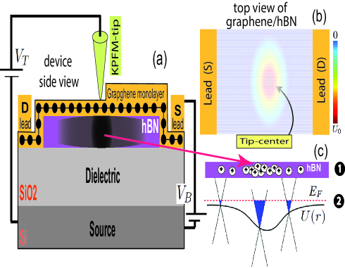
We consider a graphene/hBN heterostructure as shown in Fig. 1(a). A charge current at the graphene surface is controlled by the bias voltage applied between the source (S) and drain (D) leads. The KPFM tip acts as a top gate and tunes the potential, which induces an electric field that forms a stationary distribution (see Fig. 1 (c)) of the charges on the hBN substrate [18, 21, 20]. To evaluate the resulting screened potential several authors have solved the Poisson equation self-consistently assuming a KPFM-induced voltage pulse and radius . At zero magnetic field, the screened potential is modeled by [18, 21, 20]:
| (1) |
where is the discretized distance of the graphene sites from the center of the KPFM tip. We denote by the electric potential at the center and its corresponding radius. The third term defines the background value and can be controlled (cancelled out) by a back-gate voltage [21, 20].
The model potential , in Eq. (1), is used in a tight-binding Hamiltonian to investigate the valley transport properties in the presence of the tip-induced potential. We adopt a tight-binding model in a honeycomb lattice holding a single orbital per site and neglect the chemical bonding or any modification in the atomic structure of graphene and hBN layers [28, 29]. The resulting Hamiltonian that describes the system is given by
| (2) | |||||
where and are the creation and annihilation operators for an electron in graphene sublattice A (B) at sites and , respectively. The hopping energy is denoted by and the on-site term is set to zero (Fermi level). The heterostructure introduces an additional second term which describes the induced sublattice gap that arises mainly from the presence of the hBN substrate beneath the graphene layer [28, 29].
Theory and experiments have been analyzed and compared in the presence of a STM or KPFM tip, and have shown that the screened potential depends on the radius of the KPFM tip. For a Gaussian shape they have used the range nm nm [30, 31, 32, 33]. Similarly, we will consider a graphene/hBN channel with zigzag edges, width nm, and length nm. Further, we take eV and meV [29, 34, 35], a tip radius nm, and since the value of can be controlled by a gate voltage [20, 21].
III Results and discussion
Below we discuss how the Fermi energy and the induced KPFM potential lead to valley filtering when only one valley channel is active and some conditions are fulfilled/ We compute the transmittance of each valley and show that the relevant conditions concern mainly the signs of and and their ranges.
III.1 Electron-hole symmetry broken by the KPFM tip potential
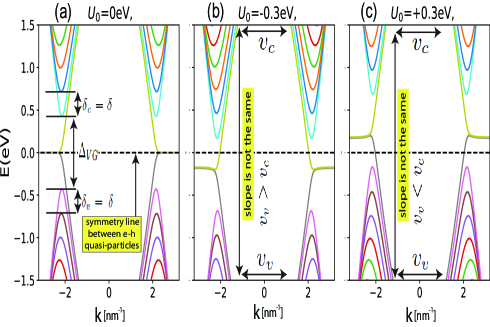
Before stepping into the process of valley filtering and investigating the parameters that affect and monitor the valley transport in the presence of the induced electrostatic potential, we start by showing the dispersion relation for zigzag boundaries of the honeycomb lattice in Fig. 2. For operating valley filtering, it is important to have propagating modes at both valleys. This is achievable in a 2D zigzag strip, when is higher than , where is the valley-mode spacing gap, as shown in Fig. 2 (a). For this reason, the valley-dependent conductances in the system can be addressed independently only beyond this limit defined by what we call the valley-mode gap with both the and channels propagating.
Additionally, it is clearly observed from the band spectrum in Fig. 2 (b) and (c) that the electron-hole symmetry is broken by the induced potential, where the conduction and valence bands are not affected simultaneously by the same value of induced potential (non-vanishing value for the potential at the border of the system due to the finite size of the system). In fact, positive values of the induced potential affect the quasi-particles for while the negative ones affect them only for . This broken symmetry between the quasi-bound states in the valence and conduction bands creates the correct conditions for operating valley filtering of the propagating carriers at a given and the Fermi velocity plays a major role in selecting valley current as will be illustrated below.
To resolve different transport channels in -space, where the electron transmission probability of each Dirac cone is observed separately, we adopt the tight-binding model in Eq. 1, and we define the valley conductance and related to the current flow across the induced potential at given Dirac cones and , respectively. More details about computing valley conductance are discussed in Appendix. A.
To investigate the dependence of the valley conductance in terms of the Fermi energy and tip-induced potential pulse , we consider two cases: (1) the valley conductance is considered in terms of for a fixed value of ; (2) the valley conductance is considered in terms of for a fixed value of .
III.2 Valley conductance in terms of the Fermi level
We have calculated the valley-dependent transmission at each valley independently for fixed tip potential meV and meV. The Fermi energy of the incident electrons varies between meV and meV and numerical results for the valley conductance, as a function of , are shown in Fig. 3.
It is clear that by tuning the Fermi energy one could operate a valley filter in a none symmetric energy range and within the first propagating mode defined by the energy mode . Depending on the sign of the induced potential and within an energy range, only one valley channel is allowed to pass. According to Fig. 3, the valley filtering happens when is increased beyond the energy limit . We find that, for positive values of the induced potential, as shown in Fig. 3 (a) and (b), only one valley is allowed within the energy range meV with meV ( meV) for meV ( meV). We observe that of the conductance results from the flow of electrons at () for positive , while of the conductance results from the flow of electrons at both valleys for negative .
The presence of the electrostatic potential induced from the KPFM tip does affect the quasi-bound states in the valence or conduction bands depending on the bias sign, as shown in Fig. 2 (b) and (c). Consequently, the propagating modes of the electron quasi-particles (at positive energy) and hole quasi-particles (at negative energy) behave differently. As a result, valley-dependent transport, when the electron-hole symmetry is broken , will depend on the sign of and . For instance, for , at positive the propagating modes are affected by the induced potential, and valley-dependent transmission occurs . However, at negative the propagating modes shift from the conduction to the valence bands, as shown in Fig. 2 (c). This interband transition is not affected by the induced potential when is positive, and hence no valley-dependent transmission occurs at . Similarly, for negative induced potential, the electron propagating modes belonging to the conduction bands are not affected while the quasi-bound states in the valence bands are. Summarizing, valley filtering happens at and destroyed at .
On the basis of the above arguments, a valley-dependent transmission, i.e., a selective population of a single valley, is pronounced depending on the sign of and . In more detail, we contrast the slopes in the dispersion relations of the valence and conduction bands according to the signs of and the induced potential. This contrast does explain the presence (absence) of valley filtering at for positive (negative) values of . More precisely, for a given this slope does affect the Fermi velocities depending on the sign of as shown in Fig. 2. To confirm this assertion, we refer again to the dispersion relation, for zigzag boundaries, where we express the Fermi velocities in terms of the mode spacing or valley-mode gap as
| (3) |
where m/s is the Fermi velocity in pristine graphene. In our case, with the tight-binding parameters and sample shapes specified in Sec. II, we have meV, where . Hence, the mode spacing is straightforwardly derived from the velocity and vice versa.
One important remark that we might also highlight from the output of Fig. 3 is the presence of an oscillatory behavior that is valley dependent. Indeed, the oscillations near the vicinity of the mode opening energy is appearing due to the potential in the scattering region, where only few-mode (valley-dependence) are affected by the potential landscape of the GQDs and behave similarly to the Fabry-Perot oscillation [36]. More precisely, the conductance oscillations are valley-dependent and many features of conductance oscillations are similar to the resonant tunneling in quantum antidots [37, 38]. Importantly, as shown in Fig. 3, () valley modes are affected by tip-potential landscape and feature conductance oscillations at negative (positive) Fermi levels where the resonance increases proportionally with induced potential and happens only within the valley-mode gap when both and have the same polarity.
III.3 Valley conductance in terms of the induced potential
When a tip potential is induced, the Fermi velocity, at positive or negative incident energy around the tip-induced potential is no longer the same and becomes a function of .Indeed, The presence of the contacts (left and right reservoirs) makes the system finite and therefore the tip’s induced potential doen’t vanish near the leads. One has to consider that remanescent component of the potential in the lead and thus ends up with a band structure with different Fermi velocities (, ) at the conduction and valence bands.
We bear in mind that the Fermi wavelength is inversely proportional to the Fermi velocity . The conductance is very sensitive to the variation of (especially for large quantum dots). In fact, far from the modes opening, the Fermi velocity approaches that of infinite pristine graphene and therefore it barely varies. In contrast, near the mode opening, where the band is highly non-linear, the Fermi velocity varies a lot with and this explains why depending on the sign of (,) and therefore, as we can deduce from the band structure, the filtering can happen or not.
Now let us go back to Fig. 3 and discuss the range of valley filtering. It is seen that by increasing the value of the induced potential from meV to meV, the energy range of the valley filtering increases since the energy mode is sensitive to the value of () and steps from meV to meV, respectively. From Fig. 2 and Fig. 3, we infer that for positive and , the electron propagating modes are strongly affected and the energy mode meV) meV) where the conductance exhibits a smooth less quantized plateaus. For negative the modes are not affected by where meV) meV), and hence the conductance exhibits quantized plateaux at an odd number of where stands for spin degeneracy. However, for negative induced potential, the process is entirely inverted because for negative the propagating modes are strongly affected whereas for positive they are not.
III.4 Rules for operating selective valley current
The analysis of Sec. III.1 and III.3 showed that valley filtering is allowed only when the sign of the product () is positive. Indeed, beyond the valley-mode spacing gap () in Fig. 3, we showed that a positive (light gray background) product leads to valley filtering of the current while a negative one (dark-gray background) destroys the valley filtering process.
This is also shown in Fig. 4, where we plot the valley current in terms of and and maintain the product positive.
In more detail, we set the sign of the same as and then select a positive (negative) value of between and , cf. Fig. 3. Once these conditions are fulfilled, we map the current of the propagating channel at and . The corresponding current is evaluated and mapped in Fig. 4.
As illustrated in Fig. 4, the valley filtering process is operative due to the positive sign of the product . Interestingly, the currents for both positive and negative are equal, but the opposite energy sign shifts the valleys with only one valley allowing current to flow and the other one blocking it. Hence, depending on and , one can break the valley degeneracy and generate a valley-polarized current. This is an important result as it leads to valley selection by changing either or a bias gate which shifts or changes its sign.
Below we will show that the valley filtering can also take place for some potentials and either sign of the product . This valley filtering does correspond to resonances with some states affected by the induced potential.
III.5 Valley filtering and resonances
As mentioned above, the tip-induced potential breaks the symmetry between the valence () and conduction () bands and the valley-polarized conduction becomes sensitive to its sign and strength for a given . In Fig. 5 (a) and (b) we show the conductance as a function of .
First, as in section III.3, the results show that the valley filtering depends on the sign of the product which is the key point for breaking the valley degeneracy and creating a valley-polarized current. For instance, for and at meV, the conductance is polarized for in the range meV with only the channel conducting. However, for meV the valley-selecting process is reversed and only the channel is conducting for in the range meV.
Second, for the obtained results show valley anti-resonances (and resonances) where the conductance drops to zero with respect to valley conductance at only one Dirac cone ( or ). This process can be justified due to valley confinement, known as Klein’s tunneling [20, 39, 40]. More precisely, to show the presence of confined states we employ the kernel polynomial method (KPM) to numerically compute the local density of states (LDOS) using Chebyshev polynomials [42, 43] along with damping kernels [44] as recently provided by a Pybinding package [45]. To compute the LDOS we count the sites contained within the shape of the induced potential, determined by . We observe that the electron are almost localized at induced potential landscape, where the superposition of the confined states wind up with the features of vortex pattern which does appear at the induced potential boundaries.
The same remarks as in Fig. 4, can be drawn from Fig. 5(c) and (d) where the LDOS for and are equal, where the opposite energy sign shifts only the valleys with only one valley confined. Hence, depending on and , one can break the valley degeneracy and generate valley confined states when the product is negative.
The resonance at meV (meV) occurs for negative (positive) and results from confined states of the quasi bands in the valence (conduction) band.
The main point here is that we confirm and show that the states in the case meV (meV) are indeed resonant states with a high local density within the area that defines the GQDs. In our case, the interference might happen inside the induced island due to the shape of GQDs with specific values of induced potential.
Since we are dealing with electron-hole broken symmetry, positive and negative energy bands are affected independently by the induced potential. Also, since the ribbon width is finite, the momentum is discretized. Therefore, the anti-resonances for (dark gray area in Fig. 5 (a) and (b)), can be clearly identified and appear nearly periodic. Since does affect the set of discrete values in momentum space, we can state that different values of lead to a different set of resonances with their number depending on the values of and .
III.6 Robustness of valley filtering against disorder and strip width
Operating valley filtering controlled by either or must be robust against a disorder potential. For this purpose, in Fig. 6, the valley polarization is plotted as a function of in the presence of an on-site disorder of strengths . The relevant Hamiltonian is , where is defined in Eq. (2) and are numbers randomly distributed in the range . We will consider a strong disorder .
We notice that the disorder does not affect the polarization even for values stronger than . For all considered disorder strengths, Fig. 6 shows that a valley filtering is always present and robust against on-site disorder.
Additionally, we have also considered the effect of the ribbon width and plotted, in Fig. 7, the valley conductance versus for several widths , determined by the ratio , for a Gaussian shape with nm. We focus on the side on which and valley filtering operates as discussed previously. We notice that the valley filtering is more evident for . More precisely, for , , we have, respectively, the energy ranges , and meV, where the () signs are for meV ( meV), respectively. From Fig. 7(a) and (b), we can see that the conductance plateaux are flatter for than for . Additionally, from Fig. 7(c) and (d) we clearly observe that by increasing the ratio the energy range of controlling the valley filtering decreases and it might vanish for since falls between and . More precisely, for the polarization drops and we have for .
IV summary and conclusions
We presented an approach for operating valley filtering based on the KPFM-induced potential that opens various roads to experimental verification. Using such an electrostatic potential, instead of PMFs induced from nanobubbles, we can operate or destroy the valleys filtering depending on the signs of the electron energies and the induced potential. A positive sign of their product () allows operating valley filtering, and the bias voltage, which controls the energy sign, shifts the valleys while only one of them allowing current to flow and the other one blocked.
We have also noticed the presence of conductance oscillations near the vicinity the mode opening energy, which are valley dependent and whose strength is proportional to that of the induced potential within the mode-spacing gap. These oscillations are similar to those in resonant tunneling in quantum antidots and to the Fabry-Perot ones. Furthermore, valley polarized currents can occur for negative products . In such a case the valley filtering does correspond to resonances; some states are affected by the induced potential and only propagating states belonging to one valley confined in the induced GQDs occur.
To the best of our knowledge, we are the first to realize that the valley is controlled and might be processed by the rule defined by the sign of , where the interplay between the sign of and that of the tip-induced potential provides an alternative example of valley filtering. The results of the present study can facilitate the development of valleytronic devices.
Acknowledgments. The authors acknowledge computing time on the SHAHHEN supercomputers at KAUST University.
Appendix A Valley-dependent transmission and polarization
Below we briefly describe the derivation of the valley-dependent transmittance and polarization expressions. The propagating modes in the leads can be selected depending on their velocity and momentum direction. This is achieved using the Kwant functionalities [47] that couple the propagating modes with the scattering region and therefore allow the evaluation of valley transport properties. We consider only propagating modes and assume that valley modes are defined based on propagating states [47]. These states are characterized by both degrees that contain the two valleys (obtained from ) and (obtained from ) in the graphene lead [14, 12]. Once the valley states are defined, we resolve different transport channels in reciprocal space, with the electron transmission probability at each Dirac cone computed separately. Within the Green’s function approach [48, 49] the valley-resolved channels lead to the total transmittance of electrons , where the valley transmittance given by
| (A.1) |
The Green function matrices are given by
| (A.2) |
and
| (A.3) |
is the imaginary part of the self-energy of the contact given by coupling, independently, the scattering region (defined by the Hamiltonian ) with each valley mode. For more details see Ref. [14, 46]. Once the valley-dependent transmission is derived, we define the valley conductance and at the Dirac cones and , respectively as To obtain both valley modes and ensure valley-resolved channels, we consider the propagating modes for (cf, Fig. 2). After obtaining them the two valleys can be separated depending on their momentum sign. The resulting valley polarization is obtained as
| (A.4) |
For the electrons are localized entirely at the valley and full polarized transmittance is ensured. corresponds to unpolarized electrons.
We might also obtain the local density of states (LDOS) at a given sample site as:
| (A.5) |
the energy is the energy of the confined states where somation goes over all electron eigenstates of the Hamiltonian in Eq. 2 with energy . The quantity in Eq. A.5 is numerically computed using Chebyshev polynomials [42, 43] and damping kernels [44].
Appendix B Valley current mapping
We adopt the procedure detailed in the Kwant package [47]. The density operator and continuity equation are expressed as
| (B.1) |
is the Hamiltonian of the heterostructure in the scattering region whose size is sites and is the eigenstate of the propagating mode of the graphene’s lead whose size is . Here defines all sites or hoppings in the scattering region and is the current.
For a given site of density , we sum over its neighbouring sites b. Then the valley current takes the form
| (B.2) |
and
| (B.3) |
where is a matrix with zero elements except for those connecting the sites a and b. In this case, the hopping matrices in the heterostructure are obtained from the first term of Eq. 2.
text REFERENCES
References
- [1] F. Herling, C. K. Safeer, J. Ingla-Aynés, N. On-toso, L. E. Hueso, and F. Casanova, APL Materials. 8, 071103 (2020).
- [2] W. Savero Torres, J.F. Sierra, L.A. BenÃtez, F. Bonell, J.H. GarcÃa, S. Roche, and S.O. Valenzuela.Magnetism, MRS Bulletin. 45, 357 (2020).
- [3] K. Zollner, A. W. Cummings, S. Roche, and J. Fabian, Phys. Rev. B. 103, 075129 (2021).
- [4] Z. Fan, J. H. Garcia, A. W. Cummings, J. E. Barrios-Vargas, M. Panhans, A. Harju, F. Ortmann, S. Roche, Physics Reports. 903, 1 (2021).
- [5] J. F. Sierra, J. Fabian, R. K. Kawakami, S. Roche, and S. O. Valenzuela, Nature Nanotechnology 16, 856 (2021).
- [6] A. Belayadi and P. Vasilopoulos, Nanotechnology, 34 085704 (2023).
- [7] D. R. Costa, Andrey Chaves, S. H. R. Sena, G. A. Farias, and F. M. Peeters, Phys. Rev. B. 92, 045417 (2015).
- [8] L. L. Tao and Evgeny Y. Tsymbal, Phys. Rev. B. 100, 161110(R) (2019).
- [9] Yi-Wen Liu, Zhe Hou, Si-Yu Li, Qing-Feng Sun, and Lin He, Phys. Rev. Lett. 124, 166801 (2020).
- [10] D. Zambrano, P.A. Orellana, L. Rosales, and A. Latgé, Phys. Rev. Applied 15, 034069 (2021).
- [11] F. de Juan, A. Cortijo, M. A. H. Vozmediano, and A. Cano, Nat. Phys. 7, 810 (2011)
- [12] Mikkel Settnes, Stephen R. Power, Mads Brandbyge, 1 and Antti-Pekka Jauho, Phys. Rev. Lett. 117, 276801 (2016).
- [13] S. P. Milovanovic and F. M. Peeters, Appl. Phys. Lett. 109, 203108 (2016).
- [14] Thomas Stegmann and Nikodem Szpak, 2D Mater. 6, 015024 (2019).
- [15] D. Gunlycke and C. T. White, Phys. Rev. Lett. 106, 136806 (2011).
- [16] D. Gunlycke and C. T. White, J. Vac. Sci. Technol. B 30, 03D112 (2011).
- [17] Y. Liu, J. Song, Y. Li, Y. Liu, and Q.-F. Sun, Phys. Rev. B 87, 195445 (2013).
- [18] A. Orlof, A. A. Shylau and I. Zozoulenko, Phys. Rev. B 92, 075431 (2015).
- [19] Nils M. Freitag, Larisa A. Chizhova, Peter Nemes-Incze, Colin R. Woods, Roman V. Gorbachev, Yang Cao, Andre K. Geim, Kostya S. Novoselov, Joachim Burgdorfer, Florian Libisch, and Markus Morgenstern, Nano Lett 16, 5798-5805 (2016).
- [20] Wyatt A. Behn, Zachary J. Krebs, Keenan J. Smith, Kenji Watanabe, Takashi Taniguchi, and Victor W. Brar, Nano Lett 21, 5013-5020 (2021).
- [21] SY. Li and L. He, Front. Phys 17, 33201 (2022).
- [22] G. Giavaras, P. A. Maksym, M. Roy, J. Phys 21, 102201 (2009).
- [23] G. Giavaras, F. Nori, Phys. Rev. B 85 85, 165446 (2012).
- [24] L. A. Chizhova, F. Libisch, J. Burgdorfer, Phys. Rev. B 90, 165404 (2014).
- [25] S. Y. Li, Y. Su, Y. N. Ren, and L. He, Phys. Rev. Lett. 124, 106802 (2020).
- [26] P. A. Maksym and H. Aoki, Phys. Rev. B 88, 081406(R) (2013).
- [27] S. Samaddar, J. Coraux, S.C. Martin, B. Grevin, H. Courtois, C.B. Winkelmann, Nanoscale 8, 15162-15166 (2016).
- [28] J. M. Marmolejo-Tejada, J. H. Garcia, M. Petrovic, P.H. Chang, X.L. Sheng, A. Cresti, P. Plechac S. Roche, B. K. Nikolic, J. Phys. Mater 1, 015006 (2018).
- [29] G. Giovannetti, P. A. Khomyakov, G. Brocks, P. J. Kelly, J. van den Brink, Phys. Rev. B 76, 073103 (2007).
- [30] P.A. Maksym, M. Roy, M.F. Craciun, S. Russo, M. Yamamoto, S. Tarucha, H. Aoki,. J Phys Conf Ser 245,012030 (2010).
- [31] J. Lee, D. Wong, J. Velasco, J.F. Rodriguez-Nieva, S. Kahn, H.Z. Tsai, T . Taniguchi, K. Watanabe, A. Zettl, F. Wang, L.S. Levitov, M.F. Crommie , Nat Phys 12,1032 (2016).
- [32] N.M. Freitag, L.A. Chizhova, P. Nemes-Incze, C.R. Woods, R.V. Gorbachev, Y. Cao, A.K. Geim, K.S. Novoselov, J. Burgdorfer, F. Libisch, M. Morgenstern, Nano Lett 16, 5798 (2016).
- [33] H. V. Grushevskaya, G. G. Krylov, S. P. Kruchinin, and B. Vlahovic, (eds) Nanostructured Materials for the Detection of CBRN. NATO Science for Peace and Security Series A: Chemistry and Biology. Springer, Dordrecht.
- [34] W. Yao, S. A. Yang, and Q. Niu, Phys. Rev. Lett. 102, 096801 (2009).
- [35] Y. Ren, Z. Qiao, and Q. Niu, Rep. Prog. Phys. 79, 066501 (2016).
- [36] V. J. Goldman and B. Su, Resonant tunneling in the quantum Hall regime: Measurement of fractional charge, Science 267, 1010 (1995).
- [37] S.M. Mills, A. Gura, K. Watanabe, T. Taniguchi, M. Dawber, D.V. Averin, X. Du, Phys. Rev. B 100, 245130 (2019).
- [38] F. E. Camino, Wei Zhou, V. J. Goldman Phys. Rev. B 76, 155305 (2007).
- [39] C. Gutierrez, L. Brown, C.J. Kim, J. Park, A. N. Pasupathy, Nat. Phys 12, 1069-1075 (2016).
- [40] P. G. Silvestrov and K. B. Efetov, Phys. Rev. Lett 98, 016802 (2007). trostatically confined Dirac fermions in graphene quan- tum dots, Nat. Phys. 12(11), 1032 (2016).
- [41] John P. Boyd, Chebyshev and Fourier Spectral Methods. Mineola, 2nd ed., Dover, New York (2001).
- [42] Alexander Weibe, Gerhard Wellein, Andreas Alvermann, and Holger Fehske, Rev. Mod. Phys 78, 275 (2006).
- [43] A. Ferreira and E. Mucciolo, Phys. Rev. Lett 115, 106601 (2015).
- [44] A. Weibe, G. Wellein, A. Alvermann, and H. Fehske, Rev. Mod. Phys 78, 275 (2006).
- [45] Moldovan D, An.elkovic M, Peeters FM. 2017 Pybinding V0.9.4: A Python Package For Tight-Binding Calculations. DOI 10.5281/zenodo.594754.
- [46] Stegmann22W. Ortiz, N. Szpak, and T. Stegmann, Phys. Rev. B 106, 035416 (2022).
- [47] C. W. Groth, M. Wimmer, A. R. Akhmerov, X. Waintal, Kwant: a software package for quantum transport, New J. Phys 16, 063065 (2014).
- [48] M. Istas, C. Groth, A.R. Akhmerov, M. Wimmer and X. Waintal, SciPost Phys. 4, 026 (2018).
- [49] T. Ozaki, K. Nishio and H. Kino, Phys. Rev. B 81, 035116 (2010).