At present at ]Department of Condensed Matter Physics, Weizmann Institute of Science, Israel.
Superconductivity in thin films of RuN
Abstract
Superconductivity has been found in RuN films obtained by reactive magnetron sputtering. This is a novel member of the metal nitride superconductors family. The critical temperature of the superconducting transition varies depending on the substrate and ranges from 0.77 K to 1.29 K. The parameters of the crystal lattice of superconducting films have been determined: the lattice is distorted cubic with parameters Å, . A zero temperature upper critical magnetic field and the coherence length were found from the experimental data using WHH model. = 2.3 T- 4.1 T for different substrates and exceeds the upper paramagnetic limit, as well as 9–12 nm. An s-wave single band energy gap meV was revealed by self-field critical current experiment at temperatures down to 10 mK, exceeding the BCS ratio 3.5.
I Introduction
Transition metal nitrides have been attracting the interest of researchers for decades due to the a wide variety of their electronic properties [1]. Moreover, many of metal nitrides are superconductors with a relatively high critical transition temperature , which turns out to be higher than the critical temperature of the initial element, the transition metal [2]. The superconducting properties of niobium and titanium nitrides are best studied, and to a lesser extent nitrides of most other transition metals: zirconium, vanadium, hafnium, molybdenum, tungsten, tantalum and rhenium. At the same time, due to the complexity of synthesis [3], the superconducting properties of nitrides of platinum group metals remain poorly understood.
RuN films can be obtained by various methods: laser ablation of ruthenium in a nitrogen atmosphere [4], reactive magnetron sputtering [5, 6, 7, 8, 9]. The material is characterised by a positive enthalpy of formation. As a result, it is not stable against heating and loses nitrogen when heated above 200 ∘C [6, 9]. Consequently, no nitrogen is detected in films grown by reactive magnetron sputtering if the substrate temperature exceeds 100 ∘C [9]. NaCl-like structure was reported for films deposited by pulsed laser deposition [4] and ZnS-like structure for ones grown by magnetron sputtering [7, 8].
To the best of our knowledge, there is no information on the superconductivity of RuN films in the literature. In this paper, we demonstrate the presence of superconductivity in RuN thin films and present the main characteristics obtained by studying the crystal structure using X-ray diffraction analysis, elemental composition using energy-dispersive spectroscopy, energy structure using density functional theory, and superconducting state parameters derived from measurements of critical temperature and current, depending on the magnetic field.
II Film Growth, Their Structure and Composition
II.1 Film growth
RuN films were grown by reactive magnetron sputtering in a pure nitrogen atmosphere on substrates of various types: single-crystal silicon (Si), thermally oxidized single-crystal silicon (Si/SiO2), and quartz glass (SiO2). Film deposition was carried out in a VON ARDENNE LS 730S setup. The residual gas pressure in the chamber and the nitrogen pressure were and mbar, respectively, at a discharge current of 70-80 mA. The typical film thickness was around 100 nm. The films under study were deposited at room temperature in a single technological circle.
II.2 Film composition
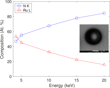
Figure 1 shows the elemental composition of a RuN/Si film obtained by the energy-dispersive X-ray spectroscopy (EDS) at different electron energies. We see that EDS results depends on the e-beam energy. This dependence corresponds to a shift of the effective analysis area deeper into the substrate with the e-beam energy increase (the substrate contribution at 20 keV is dominant) and temperature instability of the films around 200 ∘C observed earlier [6, 9]. The damage produced by e-beam during collecting EDS data at large energies is clearly seen in SEM images of the film surface (see inset in Fig. 1). The study of the elemental composition of the RuN films, the superconducting properties of which were investigated, carried out at an electron energy of 4 keV at which the substrate contribution does not exceed a few percent, gave the following composition: 50.3 at.% of Ru and 49.7 at.% of N.
II.3 Films structure study
Structural studies were carried out on a Panalytical MRD diffractometer with a parabolic X-ray mirror as the primary monochromator and a third parallel analyzer. The samples were attached to a crystal holder made of single-crystal silicon to reduce the background.
Figure 2 shows square scale X-ray diffraction patterns of a RuN film on a silicon substrate obtained with a joint –-scan (blue) and with a fixed sample at an angle of for scans (brick red). In the first case (blue), the reflecting planes are parallel to the substrate surface; in the second case, they are inclined to the surface (brick red). In the range of angles on the red curve, one of the two peaks disappears whereas the intensity of the peak at an angle of on the red curve increases, which indicates the existence of a preferential grain orientation parallel to the substrate surface. Unfortunately, an asymmetric silicon peak with a sharp increase in intensity partially overlaps with the red curve.
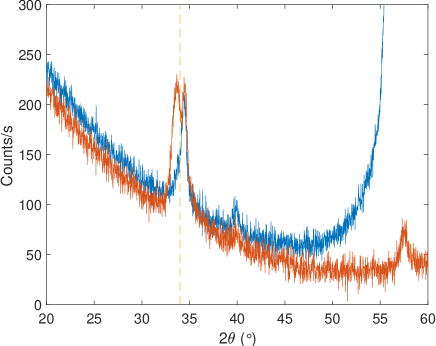
Figure 3 shows reflectometric curves of RuN films on silicon (blue) and SiO2 (red) substrates. Ruthenium has a very high density (12.41 g/cm3) compared to silicon (2.328 g/cm3) or SiO2 (2.64 g/cm3). The greater the density, the greater the value of the angle of total external reflection, the greater the difference between the densities of the layer and the substrate, and the greater the intensity of the satellites. In RuN/Si, the density is noticeably lower than in RuN/SiO2 where the experimental reflectometric curve agrees with the calculated one (black). In addition, satellites are completely absent on the blue curve, and the decrease in intensity with increasing diffraction angle corresponds to a roughness of more than 10 nm. Reflectometry does not distinguish between the roughness of the upper surface and the diffusion smearing of the interface between the substrate and the layer. However, a decrease in density unambiguously testifies in favor of strong diffusion mixing of the composition of the epitaxial layer with the substrate.

Figure 4 shows a diffractogram of the RuN/SiO2 film. It consists of two orders of the same reflection and clearly indicates a tendency for the material to orient itself with its basal plane along the surface of the substrate.

The rocking curve of the RuN layer on SiO2 for the first reflection in the diffraction pattern is shown in the inset in Fig. 4. The maximum intensity coincides with the diffraction angle. This means that the epitaxial layer grows on an amorphous substrate with a basal plane nearly parallel to the substrate plane. In other words, it is an axial texture in which the normals to the basal plane of individual crystallites are approximately parallel, and the remaining normals to the asymmetric reflecting planes of the crystallites are evenly distributed circularly.
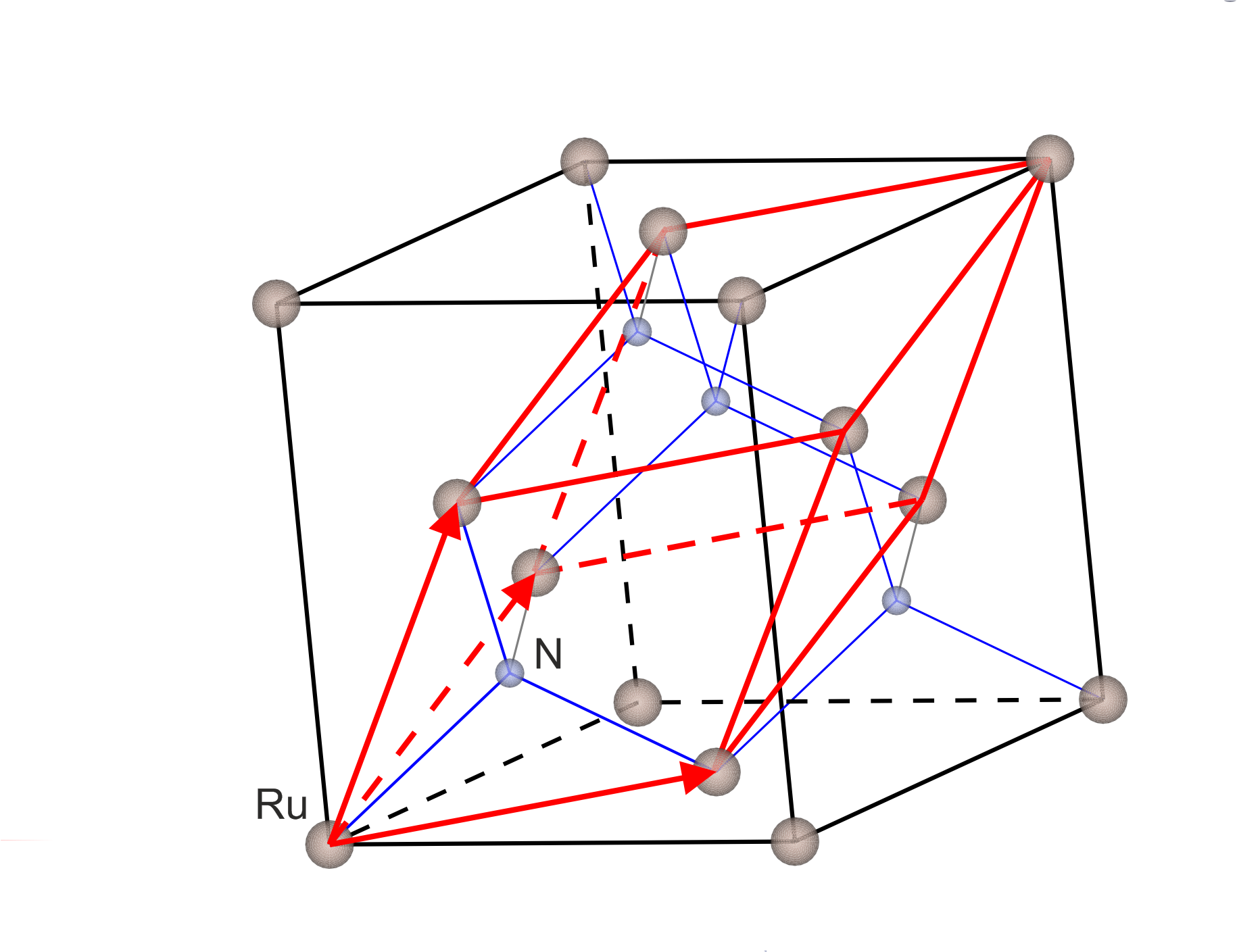
First of all, it is desirable to understand a syngony RuN structure obtained and to calculate the unit cell parameters. Ruthenium is better known in the hexagonal lattice Å, Å, but there is also a cubic variant Å.
Let’s start with the more common hexagonal structure, especially since there is a tendency for the layer to crystallize with the basal plane parallel to the substrate. If nitrogen does not change the hexagonal structure, then the first reflection perpendicular to the basal plane has the index (0002) allowed for the hexagonal structure and the value of the lattice parameter along the axis is Å. Then, the strong reflection with Å located near the first reflection can be the reflection with Å, but the slope angle for it according to the crystallography formulas is instead of the experimentally observed angle of . For reflection with Å . No other reflections of the hexagonal phase are suitable for explaining the observed experimental data.
If the layer lattice is cubic, then the first symmetric reflection has indices (111) and Å for Å. In a cubic lattice, there is only one family of planes , and , forming an angle of with the (111) plane, with the same interplanar spacing, and hence the same diffraction angle. But the experimental value of the interplanar distance for asymmetric reflections is smaller since the first pair of strong reflections on the diffraction pattern is bifurcated ( Å, Å). A possible explanation is the following: the cubic lattice undergoes rhombohedral deformation (the cube lattice is elongated along one spatial diagonal [111], as a result of which the length of the lattice changes slightly, and the angles of the unit cell become less than ). Let us find the magnitude of the deformation of the corners from the bifurcation of the first two reflections. For Å and Å in terms of interplanar distances and the angle between them, they correspond to the lattice Å, . The calculated angle of inclination of the three planes , and to the (111) plane is , which is close to the experimental value of , taking into account the grain misorientation half-width of . Let’s check this conclusion on other reflections.
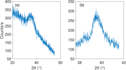
The reflection in Figs. 5(a),(b) with an angle of inclination to the basal plane of and an angular position of , Å can be identified as the reflection (022) with calculated Å and an inclination angle of , while for an undeformed cubic lattice the inclination angle is . Little discrepancies can be associated with the layer defects, which iconcentration is noticeably greater in the layer on silicon, due to which the maxima of the far reflection on the two substrates noticeably diverge (, ).
Thus, all RuN reflections observed on the diffractograms belong to a cubic lattice deformed along one spatial diagonal, with parameters Å, .
III Numerical simulation of electronic band structure
The electronic band structure and Fermi surface calculations were performed using the Abinit package [10]. Conventional unit cell with the R3m:H orthorombic symmetry [11] obtained above can be reduced to primitive unit cell with parameters Å and (Fig. 6). Structure optimization was performed with full unit cell optimization. Lattice vector lengths were reduced by 0.05 Å(1.5%) and reangle was increased by (4%) after optimization. We used original lattice parameters obtained from the experiment for the electron band structure calculations.
The calculations were performed in the framework of density functional theory (DFT) and based on exchange-correlation functional with the Perdew-Burke-Ernzerhof (PBE) parameterization of the generalized gradient approximation (GGA). Spin-orbit coupling (SOC) was taken into account, and non-collinear full relativistic pseudopotentials were used because of the presence of rather heavy element Ru, An energy cutoff of 600 eV and -point grid within the Monkhorst-Pack scheme were adopted for the sampling Brillouin zone.

Electron bands originating from Ru atom layers are affected by SOC, which follows from the results of RuN electronic band structure calculation (Fig. 7). SOC leads to the splitting of the electron dispersion curves, but some electronic states are kept degenerate along , and lines in the Brillouin zone. Fermi level ( in Fig. 7) crosses split dispersion curves along line and degenerate ones along and lines, which produces two Fermi surface inner and outer branches. The calculated Fermi surface outer branch is shown in Fig. 8 within the Brillouin zone. The yellow solid line on the surface in Fig. 8(a) is a cross-section line corresponding cut plane. The Fermi surface cross-section is shown in Fig. 8(b).


Electron spin density for each band and wave vector was calculated from the wave functions obtained. Spin density averaged over reciprocal unit cell is shown in Fig. 8(b) by arrows and demonstrates the opposite spin density orientation of the Both Fermi surface branches.
The density of states (DOS) presented in Fig. 9 demonstrates the metallic character of the material. It is similar to the results for cubic F43m [12] and tetragonal I42m [13] structures. Atom orbitale projected DOS curves show the main contribution of Ru atom orbitals (82%) into the DOS at Fermi energy (red curve in Fig. 9).

Electron-phonon coupling parameters and [14], which define RuN superconducting state characteristics, were calculated with the usage of Quantum Espresso package [15]. -mesh was used for self-consistent electron wave functions calculation, and -mesh was used for phonon spectrum calculation. The following values were obtained: , K.
IV Superconducting Properties of RuN Films: Upper Critical Field and Critical Current
IV.1 Upper Critical Field
Figures 10 and 11 show the results of measuring the resistive transition in ruthenium nitride films grown on a substrate of polycrystalline SiO2 (Fig. 10), silicon with an oxide layer obtained by thermal oxidation (Fig. 11, left panel) and silicon with natural oxide (Fig. 11, right panel) at various values of the magnetic field. In a zero magnetic field, these films exhibit a relatively narrow resistive transition at temperatures of 1.29 K, 0.86 K and 0.77 K, respectively, measured at the onset of nonzero resistance. The superconducting resistive transition gradually shifts to lower temperatures with an increasing magnetic field up to 1 T. It is worth noting that the width of the superconducting transition for all three samples increases significantly with increasing magnetic field, which is characteristic of hard type II superconductors, and one can expect that thermal fluctuations can play a significant role in the dissipation processes in magnetic fields.


Figure 12 shows the temperature dependencies of the upper critical magnetic field obtained from the curves shown in Fig. 10 measured at different values of the magnetic field. Four curves correspond to four standard criteria for determining ( is zero resistance, is 10% of the ”value” of the superconducting transition, , are, respectively, 50% and 90% of the transition). An increase of the width of the superconducting transition with increasing magnetic field, which is characteristic of hard type II superconductors, is clearly seen. In the measured temperature range, the curves follow the WHH model [16, 17, 18]. From the results of approximation by the WHH model, the values T and -12 nm for the zero resistance criterion have been obtained.
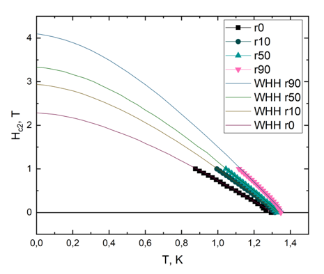
Figure 13 shows the temperature dependencies of the upper critical field for all three samples obtained from the resistive transitions in Figures 10 and 11. For clarity, we used only one criterion - r90. The inset shows the upper critical field temperature dependence in reduced coordinates: vs , so that it is clear, that even though and are strikingly different for different films, the T-dependence is the same.

The question arises as to why films deposited in a single technological process have such different values and other superconducting parameters. The results of the reflectometric study shown in Fig. 3 lead us to conclude that this difference results from film degradation caused by diffusion mixing of the film layer composition with the substrate.
IV.2 Critical Current And the Energy Gap
The ability to carry a non-dissipative current, sometimes of very high density, is one of the most valuable inherent properties of the superconductors. Not only it is an appealing attribute for practical use, but also it is a fundamental feature that gives information about the intrinsic properties of a superconductor. As was first suggested by Talantsev et.al [19], the temperature dependence of self-field critical current can be used to derive the energy gap and London penetration depth of superconductors. This model was successfully used to derive fundamental superconductor parameters in several dozens of materials, starting with conventional superconductors [19], copper-based HTSC [20], iron-based HTSC [21] and even most recently discovered superhydride HTSC [22], [23], [24].

For thin films (when the half thickness of a film is smaller than the penetration depth ), the self-field critical current density, in zero external magnetic field (when the magnetic field is generated only by the current itself) is related to the penetration depth as follows:[19],
| (1) |
where is flux quantum, and is Ginzburg-Landau parameter, which remains almost constant under the logarithm.
Since superfluid density , one can determine the temperature dependence of superfluid density by measuring self-field critical current density . Because of the practical temperature independence of ), for type-II superconductors is dependent only on , which provides a tool to extract the magnitude of the superconducting gap and even its symmetry. In particular, for -wave symmetry in a single-band superconductor:
| (2) |
Thus, combining equations 1 and 2, we can analyze our data within a model for a type II thin film superconductor with -wave single gap.
Figure 14 shows a set of current-voltage characteristics for RuN film on Si/SiO2 substrate with natural oxidation. Measurements were carried out on a dilution refrigerator with a standard 4-probe technique. To prevent overheating the current leads, we used a high-quality pulse current source (Keithley 6221) and a nanovoltmeter (Keithley 2182a). The pulse width was as low as 50 s.

Figure 15 shows the temperature dependence of the self-field critical current for RuN film on Si/SiO2 substrate with natural oxidation. The data points (blue symbols) were extracted from Fig. 14 by 0.5 mV criteria. We see that the Talantsev model [19] for 2D films with type II single gap superconductivity (light brown solid line in Fig. 15) fits the experimental data very well. Extracted energy gap value meV gives 2, which exceeds the BCS ratio 2.
V Discussion
Experimental lies in the interval from 1.29 K to 1.4 K for RuN films on a polycrystalline substrate according to Fig.10. On the other hand, can be estimated from the results of the simulation using a semi-phenomenological formula based on Eliashberg’s theory [14] with calculated and parameters. The experimental interval can be obtained at the Coulomb pseudopotential values -0.192. In these calculations, is considered as a phenomenological parameter. Conventional values of are lying in the interval from 0.1 to 0.15 [14], so calculated overestimates somewhat measured one.
Transition temperature determines upper Pauli paramagnetic limit, which has a form [K] for BCS-like superconductors [25, 26]. Measured values correspond to -2.6 T. It is known [27] that the Pauli limiting term is renormalized for strong coupling superconductors . -4.0 T for the samples considered here. A maximum value obtained from the experiment is equal to 4.1 T, which still exceeds fairly.
This high enough value of can be explained by the electron spin-orbit interaction with impurities [18]. Fermi-level electrons are mostly related to Ru atomic orbitals according to the results of DOS computation Fig. 9, and an excess Ru atom concentration over N atoms (see Film composition section) provides spin-orbit scattering centers. Moreover, the structure of RuN has no inversion symmetry, so we can’t exclude a mixing of singlet and triplet pairing in the presence of spin-orbit interaction, which increases the upper limit of as well [28]. Further study is required to reveal the nature of exceeding of the paramagnetic limit and possible contribution of triplet pairing.
VI Conclusion
In conclusion, we observed superconductivity in RuN films obtained by reactive magnetron sputtering on Si, oxidized Si, and silica glass substrates. The critical temperature of the superconducting transition ranges from 0.77 to 1.29 K, depending on the substrate. The crystal lattice is cubic with the following parameters: Å, . DFT calculations, together with the results of temperature-dependent self-field critical current measurements, prove that RuN is a single-gap superconductor with meV. The upper critical magnetic field depends on the substrate and, within the framework of the WHH model, corresponds to –4.1 T and –12 nm for the coherence length. exceeds the upper paramagnetic limit.
VII Data availability
Data will be made available on request.
VIII Declaration of Competing Interest
The authors declare that they have no known competing financial interests or personal relationships that could have appeared to influence the work reported in this paper.
Acknowledgements.
The work was supported by the Russian Science Foundation (project # 21-72-200114). The studies were carried out using the equipment of the Central Collective Use Center of the Lebedev Physical Institute of RAS. The computations in this study were performed using computational resources at the Joint Supercomputer Center, Russian Academy of Science.References
- Wang et al. [2021] H. Wang, J. Li, K. Li, Y. Lin, J. Chen, L. Gao, V. Nicolosi, X. Xiao, and J.-M. Lee, Transition metal nitrides for electrochemical energy applications, Chemical Society Reviews 50, 1354 (2021).
- Gurvitch et al. [1985] M. Gurvitch, J. Remeika, J. Rowell, J. Geerk, and W. Lowe, Tunneling, resistive and structural study of nbn and other superconducting nitrides, IEEE Transactions on Magnetics 21, 509 (1985).
- Gregoryanz et al. [2004] E. Gregoryanz, C. Sanloup, M. Somayazulu, J. Badro, G. Fiquet, H.-k. Mao, and R. J. Hemley, Synthesis and characterization of a binary noble metal nitride, Nature Materials 3, 294 (2004).
- Moreno-Armenta et al. [2007] M. Moreno-Armenta, J. Diaz, A. Martinez-Ruiz, and G. Soto, Synthesis of cubic ruthenium nitride by reactive pulsed laser ablation, Journal of Physics and Chemistry of Solids 68, 1989 (2007).
- Liao and Chou [2009] Y.-H. Liao and J.-C. Chou, Fabrication and characterization of a ruthenium nitride membrane for electrochemical ph sensors, Sensors 9, 2478 (2009).
- Wu et al. [2011] C.-Y. Wu, W.-H. Lee, S.-C. Chang, Y.-L. Cheng, and Y.-L. Wang, Effect of annealing on the microstructure and electrical property of run thin films, Journal of The Electrochemical Society 158, H338 (2011).
- Bouhtiyya et al. [2013] S. Bouhtiyya, R. Lucio Porto, B. Laïk, P. Boulet, F. Capon, J. Pereira-Ramos, T. Brousse, and J. Pierson, Application of sputtered ruthenium nitride thin films as electrode material for energy-storage devices, Scripta Materialia 68, 659 (2013).
- Cattaruzza et al. [2014] E. Cattaruzza, G. Battaglin, P. Riello, D. Cristofori, and M. Tamisari, On the synthesis of a compound with positive enthalpy of formation: Zinc-blende-like run thin films obtained by rf-magnetron sputtering, Applied Surface Science 320, 863 (2014).
- Cattaruzza et al. [2016] E. Cattaruzza, G. Battaglin, D. Cristofori, T. Finotto, P. Riello, and A. Glisenti, On the synthesis and thermal stability of run, an uncommon nitride, Surface and Coatings Technology 295, 93 (2016).
- Gonze et al. [2020] X. Gonze, B. Amadon, G. Antonius, F. Arnardi, L. Baguet, et al., The abinit project: Impact, environment and recent developments, Computer Physics Communications 248, 107042 1 (2020).
- de Cotret et al. [2018] R. de Cotret, P. Laurent, M. R. Otto, M. J. Stern, et al., An open-source software ecosystem for the interactive exploration of ultrafast electron scattering data, Advanced Structural and Chemical Imaging 4, 2198 (2018).
- Chen and Jiang [2010] W. Chen and J. Jiang, Elastic properties and electronic structures of 4d- and 5d-transition metal mononitrides, Journal of Alloys and Compounds 499, 243 (2010).
- Zhang et al. [2016] Y. Zhang, L. Wu, B. Wan, et al., Diverse ruthenium nitrides stabilized under pressure: a theoretical prediction, Sci. Rep. 6, 33506 (2016).
- Allen and Dynes [1975] P. B. Allen and R. C. Dynes, Transition temperature of strong-coupled superconductors reanalyzed, Phys. Rev. B12, 905 (1975).
- Giannozzi et al. [2009] P. Giannozzi, S. Baroni, N. Bonini, et al., Quantum espresso: a modular and open-source software project for quantum simulations of materials, Journal of Physics: Condensed Matter 21, 395502 (2009).
- Helfand and Werthamer [1964] E. Helfand and N. R. Werthamer, Temperature and purity dependence of the superconducting critical field, , Phys. Rev. Lett. 13, 686 (1964).
- Helfand and Werthamer [1966] E. Helfand and N. R. Werthamer, Temperature and purity dependence of the superconducting critical field, . ii, Phys. Rev. 147, 288 (1966).
- Werthamer et al. [1966] N. R. Werthamer, E. Helfand, and P. C. Hohenberg, Temperature and purity dependence of the superconducting critical field, . iii. electron spin and spin-orbit effects, Phys. Rev. 147, 295 (1966).
- Talantsev and Tallon [2015] E. F. Talantsev and J. L. Tallon, Universal self-field critical current for thin-film superconductors, Nature communications 6, 7820 (2015).
- Talantsev et al. [2017a] E. Talantsev, W. P. Crump, and J. L. Tallon, Thermodynamic parameters of single-or multi-band superconductors derived from self-field critical currents, Annalen der Physik 529, 1700197 (2017a).
- Talantsev et al. [2019] E. Talantsev, K. Iida, T. Ohmura, T. Matsumoto, W. Crump, N. Strickland, S. Wimbush, and H. Ikuta, P-wave superconductivity in iron-based superconductors, Scientific reports 9, 14245 (2019).
- Talantsev et al. [2017b] E. F. Talantsev, W. P. Crump, J. G. Storey, and J. L. Tallon, London penetration depth and thermal fluctuations in the sulphur hydride 203 k superconductor, Annalen der Physik 529, 1600390 (2017b).
- Troyan et al. [2023] I. A. Troyan, D. V. Semenok, A. G. Ivanova, A. V. Sadakov, D. Zhou, A. G. Kvashnin, I. A. Kruglov, O. A. Sobolevskiy, M. V. Lyubutina, T. Helm, et al., Non-fermi-liquid behavior of superconducting snh4, arXiv preprint arXiv:2303.06339 (2023).
- Sadakov et al. [2023] A. V. Sadakov, V. A. Vlasenko, I. A. Troyan, O. A. Sobolevskiy, D. V. Semenok, D. Zhou, and V. M. Pudalov, Vortex phase dynamics in yttrium superhydride yh6 at megabar pressures, The Journal of Physical Chemistry Letters 14, 6666 (2023).
- Clogston [1962] A. M. Clogston, Upper limit for the critical field in hard superconductors, Phys. Rev. Lett. 9, 266 (1962).
- Chandrasekhar [1962] B. S. Chandrasekhar, A note on the maximum critical field of high‐field superconductors, App.Phys.Lett. 1, 7 (1962).
- Schossmann and Carbotte [1987] M. Schossmann and J. P. Carbotte, Pauli limiting of the upper critical magnetic field, Phys.Rev. B39, 4210 (1987).
- Smidman et al. [2017] M. Smidman, M. B. Salamon, H. Q. Yuan, and D. F. Agterberg, Superconductivity and spin–orbit coupling in non-centrosymmetric materials: a review, Rep.Prog. Phys. 80, 036501 (2017).