Controlling Umklapp scattering in bilayer graphene moiré superlattice
Abstract
We present experimental findings on electron-electron scattering in two-dimensional moiré heterostructures with tunable Fermi wave vector, reciprocal lattice vector, and band gap. We achieve this in high-mobility aligned heterostructures of bilayer graphene (BLG) and hBN. Around half-filling, the primary contribution to the resistance of these devices arises from electron-electron Umklapp (Uee) scattering, making the resistance of graphene/hBN moiré devices significantly larger than that of non-aligned devices (where Uee is forbidden). We find that the strength of Uee scattering follows a universal scaling with Fermi energy and has a non-monotonic dependence on superlattice period. The Uee scattering is electric field tunable and is affected by layer-polarization of BLG. It has a strong particle-hole asymmetry – the resistance when the chemical potential is in the conduction band is significantly lesser than when it is in the valence band, making the electron-doped regime more practical for potential applications.
I Introduction
In a Galilean-invariant electron liquid, normal electron–electron scattering does not cause a loss of the momentum imparted to the electrons by the driving electric field; consequently, it can not lead to electrical resistance. A realistic Fermi liquid is, however, not Galilean invariant – a finite coupling to an underlying lattice provides a mechanism for the momentum relaxation of the quasiparticles via the Umklapp process [1]. Umklapp electron-electron (Uee) scattering is the fundamental mechanism that allows momentum transfer from electrons to lattice and imparts electrical resistance to the metal [2, 3, 4, 5, 6, 7, 8]. In this process, the crystal lattice gives a momentum kick to a pair of interacting electrons, backscattering them to the other side of the Fermi surface. Their quasi-momentum is conserved, modulo a reciprocal lattice vector ,
| (1) |
Here and are the initial and final quasi-momenta of the two electrons near the Fermi level, respectively, and is a non-zero reciprocal lattice vector of the crystal. This stringent conservation constraint, coupled with the lack of tunability of the Fermi wave vector, makes experimental identification of Uee processes in normal metals challenging [7, 9, 8]. Notable exceptions are heavy-fermionic systems whose large effective quasiparticle mass leads to an appreciable Uee-mediated resistance at very low temperatures ( m) [10].
In the limit of nearly free electrons, one can view the Uee scattering as a two-stage process: In the first step, an electron-hole pair is excited into a virtual state by an electron, followed by the scattering of one of these particles by the periodic lattice potential. The temperature dependence of the Uee scattering process at a finite temperature is thus set by the size of the scattering phase space () for each electron; only the quasiparticles residing within a width of order around the Fermi energy can undergo binary collisions. Consequently, the Uee contribution to the sheet resistance in goes as [11]. is a material-dependent parameter [12, 13, 14].
Note, however, that Uee need not be the only source of -resistivity in a material [15, 13, 16, 17, 18]. A claim that the dominant source of scattering is the Uee process should be backed up by a (1) quantification of the prefactor , (2) a demonstration of the scaling of , and (3) ruling out other competing mechanisms (e.g. electron-phonon scattering [18]) that can give -dependent charge scattering.
Graphene-based moiré superlattices [19, 6, 20, 21, 22, 23, 24, 25, 4] provide a system with precise tunability of the reciprocal lattice vectors (via the twist angle between the constituent layers) and the Fermi wave vectors (by controlling the carrier density through electrostatic gating). It thus provides a vast phase space in which Eqn. 1 may be satisfied, and the scaling of versus can be verified. Recent calculations (that treat both the electron–electron Coulomb interaction and the moiré superlattice potential perturbatively) predict that in aligned heterostructures of Bernal bilayer graphene (BLG) and hBN, Uee scattering processes should be the primary source of resistance [5].
In this Letter, we experimentally verify that in high-mobility moiré superlattices of BLG and hBN, Uee is the dominant source of resistance near half-filling. Our studies show that the strength of Uee depends non-monotonically on the superlattice period. This is at par with recent theoretical predictions [5] and in sharp contrast to observations in single-layer graphene-based superlattices [4]. We illustrate the tunability of strength of the Uee process (quantified by ) with displacement field, and carrier density, . Additionally, we demonstrate a strong particle-hole asymmetry in the strength of the Uee process, whose origin can be traced to the moiré potential having a much stronger effect on the valence band than on the conduction band [4, 5]. Furthermore, we demonstrate the high tunability of Umklapp resistivity with an external vertical electric field, emphasizing the potential for precise control over the electronic properties of bilayer graphene superlattices. Finally, we show that these processes are completely absent in non-aligned devices.
II Results and discussion
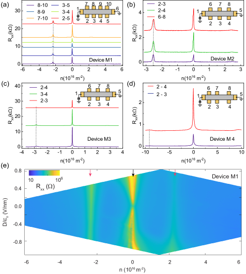
High-quality hBN/BLG/hBN heterostructures were fabricated using the dry transfer technique (Supplementary Information, section S1) [26, 27, 28]. The top hBN was aligned at nearly zero degrees with BLG, and the bottom hBN was intentionally misaligned to a large angle to ensure that a moiré pattern forms only between top hBN and BLG (Fig.1(a)). The device is in hall bar geometry (Fig.1(b)) with dual gates to tune the carrier density and the vertical displacement field independently via and . Here () is the back-gate (top-gate) capacitance, and () is the back-gate (top-gate) voltage. and are the residual number density and displacement field in the graphene due to impurities. The direction of the negative displacement field () is marked schematically in Fig.1(a). In the main text, we provide the data for a device M1 (with twist angle and superlattice wavelength nm), unless otherwise mentioned. The data for three more hBN/BLG/hBN superlattice devices, labeled M2, M3 and M4 with twist angle and respectively, and with superlattice wavelength nm, nm and nm respectively, are presented in Supplementary Information. We also present data for a non-aligned hBN/BLG/hBN device (labeled N1) to compare the -dependence of resistance between Uee-allowed (aligned devices) and Uee-forbidden (non-aligned devices) systems.
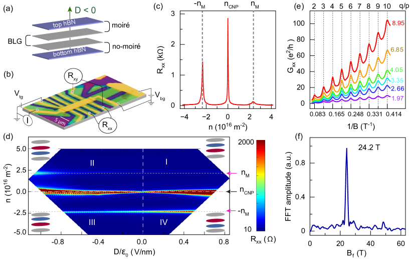
The measured longitudinal resistance on device M1, at temperature shows a peak at the charge neutrality point (CNP), and moiré satellite peaks at (Fig. 1(c)). The mobility at CNP is extracted to be . Quantum Hall measurements at a perpendicular magnetic field of T establish that both spin and valley degeneracies are lifted, indicating the high quality of the device (Supplementary Information, section S5); these measurements are used to calibrate the values of and . The angle homogeneity of the device is ascertained by comparing the data measured in different configurations (Supplementary Information, section S2).
Our results for as a function of carrier density and electric field , shown in Fig.1(d) ascertain that the values of the moiré gap in carrier density are independent of the applied electric field. The plot can be divided into four quadrants labeled I-IV. In quadrants I (, ) and III (, ), at a finite , the occupied electronic states near the Fermi energy are predominantly localized (marked with a red color oval) in the bottom layer of BLG (away from moiré interface) and are weakly localized (marked with a blue color oval) in the top layer of BLG (close to moiré interface). This leads to the suppression of moiré effects and low resistance value of satellite peak in these quadrants. The opposite effect is seen in quadrants II (, ) and IV (, ), the occupied electronic states are predominantly localized in the top layer of BLG (close to moiré interface) leading to the enhancement of moiré effects and higher resistance of the satellite peaks in these quadrants. Later in this Letter, we explore the consequences of this displacement-field-induced layer polarization on Uee scattering.
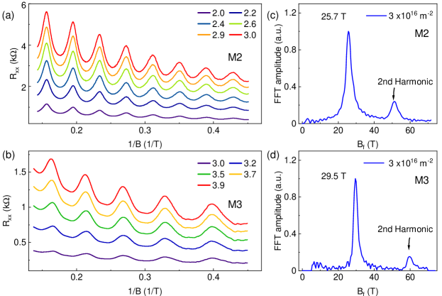
The moiré periodicity of the system is estimated from Brown-Zak oscillation measurements at (Fig.1(e)). Thermal broadening smears out Landau oscillations at this elevated temperature, and only Bloch oscillations survive [29, 30, 31, 19]. A Fourier spectrum of the oscillations yields the inverse periodicity or the ‘frequency’ of the oscillations to be T (Fig.1(f)). Observation of only a single frequency rules out the double alignment of the BLG with hBN [19, 32]. Using the relation ( being the real space area of the moiré superlattice cell, : Planck’s constant, : electronic charge), the moiré wavelength is calculated to be nm and the carrier density corresponding to filling the bands just up to the moiré gaps is ; the factor of arises from the two-fold spin-and valley-degeneracy of graphene. This value of carrier density matches exactly, validating the number density corresponding to the moiré gap obtained from zero-magnetic field measurements. The twist angle between BLG and hBN corresponding to this moiré wavelength is approximately indicating near-perfect alignment between the top hBN and the BLG.
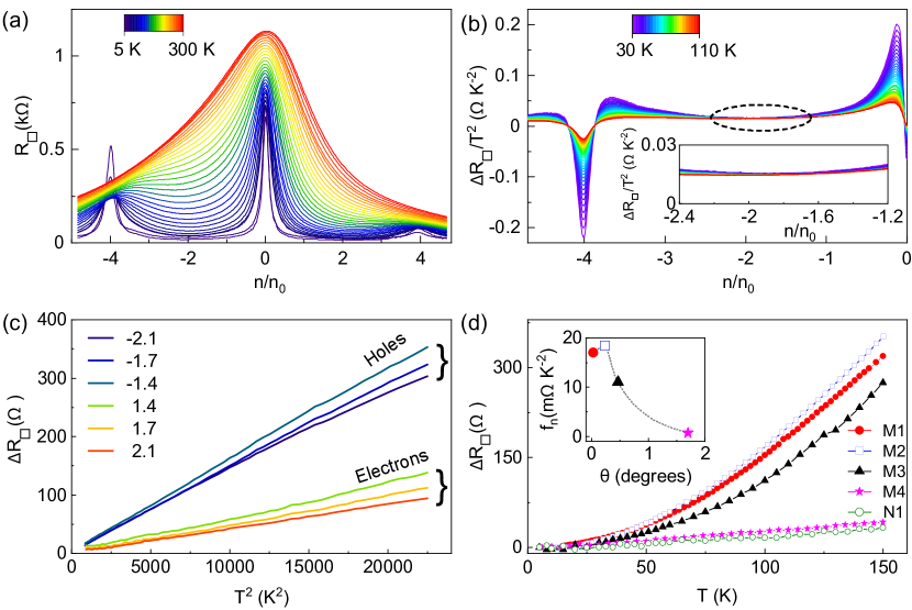
Fig. 2(a) shows the plots of the zero-magnetic field longitudinal sheet resistance ( and are the width and length of the channel respectively with ) versus the moiré band filling fraction over a temperature range at zero displacement field. Here, is the carrier density at one-forth filling of the moiré band. With increasing temperature, one notices a sharp increase in around (Fig.2(d)); this feature is completely absent in non-aligned BLG devices (Supplementary Information, section S3). As we establish below, this rapid increase in with arises from the Umklapp scattering in the device.
At , Uee is suppressed, and the resistivity is dominated by disorder scattering [12]. To mitigate the effect of static disorder scattering, we henceforth focus on . The magnitude of at is . In Fig. 2(b), we plot versus over a temperature range from to – the data at all temperatures collapse onto a single curve in the filling fraction range (marked by the dotted ellipse) showing that over this range. This can be better appreciated from the inset, which shows the data over a narrow range around . Fig. 2(c) plots the versus to better show the electron-hole asymmetry over a range of . The linearity of the plots of sheet resistance versus in this carrier density regime persists till about , establishing Uee scattering as the source of resistance (Fig. 2(c)). This temperature is of the order of the Bloch–Grüneisen temperature in graphene. Above this , electron-phonon scattering starts becoming the dominant source of resistance, and the quadratic relation between and breaks down [33, 34, 35]. Fig. 2(d) shows a comparison of for the five devices – the strong quadratic -dependence seen in aligned devices is completely absent in the non-aligned device where Uee is forbidden from phase-space arguments. Inset in Fig. 2(d) shows versus twist angle for the aligned devices, illustrating the non-monotonicity of umklapp strength on the twist angle.
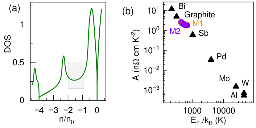
To understand the number density limits over which Umklapp processes are seen, recall that at very low , transport in graphene is dominated by electron-hole puddles [33, 36, 37]; this gives a practical lower bound of at which e-e scattering is detectable [5]. A more accurate lower limit is obtained by the constraint that the Uee process imposes on the Fermi wave vector (Eqn. 1), this sets a lower bound on equal to . (see Supplementary Information, section S4). At the other extreme, at high number densities, one begins to encounter electron-hole scattering processes at the principal mini band edges because of the moiré induced van-Hove singularity (Fig.3(b)), which masks the Umklapp scattering process [5].
Before proceeding further, we eliminate the other probable causes that are known to lead to a -dependence of the resistance. In a system with different carrier types/masses (as is the case near the primary and secondary gaps or van Hove singularities), the transfer of momentum between the two carrier reservoirs can lead to a resistivity with dependence [38, 39, 40]. This consideration guides us to avoid filling fractions that lead to Fermi levels close to these regions of the moiré bands and confine our analysis to the filling fraction range , as shown in Fig.3(a). We note that, in low-mobility dilute alloys, the thermal motion of impurity ions can also give rise to a -dependent resistance [41]; this scenario does not apply to our high-mobility heterostructures.
A phenomenological treatment, based on the Rice-Kadowaki–Woods scaling analysis [13, 14] yields:
| (2) |
In Fig.3(b), we plot ( nm is the thickness of BLG) as a function of the Fermi energy along with the compilation of data on several different materials [12]. A very good match is obtained, emphasizing the universality of the value of .
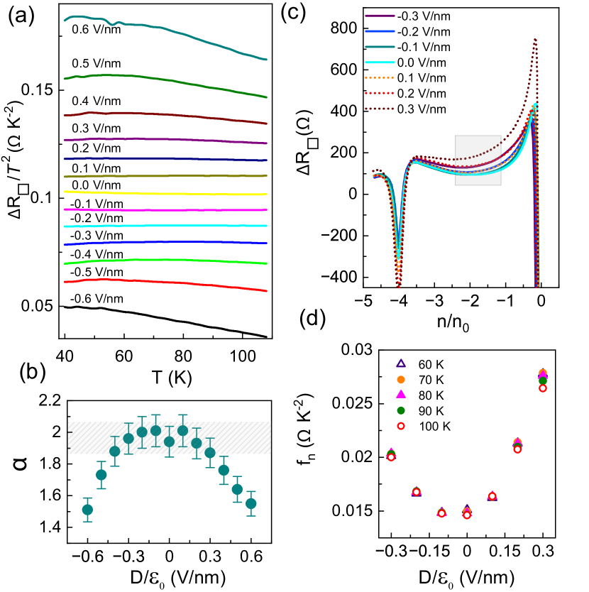
Having established Uee as the source of quasiparticle scattering in bilayer graphene/hBN moiré near half-filling (), we now shift our focus on the effect of inter-layer potential asymmetry (tuned using ) on the Umklapp scattering in the quadrant III and IV of Fig. 1(d). Fig. 4(a) plots versus for several different values of . We find that the temperature exponent of the resistance for (Fig. 4(b)). In this range of , we find a substantial increase in the scattering strength with increasing in conformity with theoretical predictions [5] (Fig. 4(c)). Fig. 4(d) plots versus over the temperature range – . These data points collapse on top of each other with growing quadratically with .
Note that has a slight asymmetry under sign-reversal of . To understand this, we recall that the sign of layer polarization in BLG depends on the direction of . A positive –field (as defined in Fig. 1(a)) increases the potential energy of electronic states in the lower layer of BLG as compared to those in the upper layer of BLG. For negative , the occupied electronic states are mainly localized in the top layer of the BLG (that forms the moiré with the hBN) [5]. For the negative –field, on the other hand, the occupied electronic states are mainly localized in the bottom layer of the BLG (that does not form the moiré with the hBN). We postulate that the combined effect of this asymmetry of layer polarization on the sign of and the asymmetry of the moiré potential inherent in this device architecture ultimately manifests as .
With further increase in the displacement field, deviates from two, indicating a suppression of Umklapp processes for . We do not have a clear understanding of the origin of this. One plausible reason can be that at large , the trigonal warping becomes strong, severely limiting the phase space over which Eqn. 1 may be satisfied [42]. A related effect of the trigonal warping is the formation of overlapping electron-hole bands at certain number densities – the scattering between thermally excited electrons and holes then masks Uee processes [5, 42]. A second possible cause of the suppression of Uee at high can be the strong modification of the BLG band by the displacement field (this includes layer-polarization, the opening of a band gap, and enhanced trigonal warping) leading to strong Zitterbewegung, which becomes the relevant scattering mechanism at large [43]. Further experimental and theoretical studies are required to verify if any of these is indeed the cause for suppression of Umklapp scattering with increasing .
III Conclusion
To conclude, our experiments unequivocally establish Umklapp scattering to be the leading source of resistance in hBN/BLG superlattices in certain filling fraction ranges. Our findings on hBN/BLG superlattice differ from recent studies on hBN/SLG superlattice [4] in several significant aspects. In SLG hBN moiré, increases monotonically with increasing superlattice period and charge carrier density [4]. In contrast, in BLG moiré superlattice is predicted to have a non-monotonic dependence on superlattice period [5]. In this Letter, we have experimentally verified this prediction. Additionally, bilayer-based systems provide strong electric field tunability of the band gap and layer polarization and thus have an enormous scope for room-temperature applications [44, 45, 46, 47, 48, 49]. We have shown that the strength of Uee increases rapidly with the increasing strength of the displacement field; this fact must be factored in when designing any -field controlled superlattice device architectures. Additionally, we find the strength of Uee scattering to be stronger in BLG/hBN superlattice than in SLG/hBN superlattice (Supplementary Information, section S6).
With the presently available technology, the best quality BLG field effect devices are formed when encapsulated between a crystalline insulator, like hBN [50, 51, 52]. As the growth of graphene in hBN leads to aligned layers [53, 54, 55], it is imperative to understand the significant sources of Joule heating in such systems for optimal room-temperature operations. Our present study achieves this and should motivate further studies in related systems like twisted bilayer graphene and twisted bilayers of transition metal dichalcogenides.
While this manuscript was under review, we became aware of a preprint [56] which demonstrates that at , transport in BLG/hBN moiré is dominated by Umklapp scattering.
Acknowledgements: A.B. acknowledges funding from U.S. Army DEVCOM Indo-Pacific (Project number: FA5209 22P0166) and Department of Science and Technology, Govt of India (DST/SJF/PSA-01/2016-17). M.J. and H.R.K. acknowledge the National Supercomputing Mission of the Department of Science and Technology, India, and the Science and Engineering Research Board of the Department of Science and Technology, India, for financial support under Grants No. DST/NSM/RD_HPC Applications/2021/23 and No. SB/DF/005/2017, respectively. M.K.J. and R.B. acknowledge the funding from the Prime Minister’s research fellowship (PMRF), MHRD. S.M. acknowledges the funding from the National post doctoral fellowship (N-PDF), SERB. K.W. and T.T. acknowledge support from the JSPS KAKENHI (Grant Numbers 21H05233 and 23H02052) and World Premier International Research Center Initiative (WPI), MEXT, Japan.
Author contributions: M.K.J., S.M., H.K.M., and A.B. conceived the idea of the study, conducted the measurements, and analyzed the results. T.T. and K.W. provided the hBN crystals. R.B., M.J., and H.R.K. developed the theoretical model. All the authors contributed to preparing the manuscript.
Supplementary Materials
S1 Device fabrication
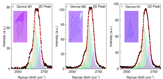
The hBN encapsulated bilayer graphene (BLG) devices were fabricated using the dry transfer technique [26, 27, 28]. Initially, BLG and hBN flakes were mechanically exfoliated onto a Si/\chSiO2 substrate. BLG flakes were first identified with optical contrast and later confirmed with Raman spectra (Fig. S1). hBN flakes of thickness ranging from nm were used in fabrication, and their thickness uniformity was confirmed using an AFM.
To make BLG-hBN single-moiré devices (labeled M1, M2, M3 and M4), the top hBN sharp edge was aligned with the sharp edge of BLG at nearly zero degrees, facilitating a moiré between BLG and the top hBN layer. The bottom hBN edge was intentionally misaligned with BLG to prevent any moiré superlattice formation between BLG and the bottom hBN layer.
In the case of a non-moiré device (N1), hBN was misaligned with both the bottom hBN and top hBN layers to prevent any moiré superlattice formation. Electrical contacts were patterned through lithography, etched with a mixture of CHF3 ( sscm) and O2 ( sscm), and contacts deposited with Cr/Pd/Au with thickness nm to form D contact with BLG. The device was etched in Hall bar geometry. Finally, The top gate was patterned through lithography, and a metal gate was deposited. Having dual gates in the devices gives control in tuning the system’s carrier density and displacement field independently.
S2 Twist angle estimation
Fig. S2 shows the plot of longitudinal resistance Rxx versus carrier density for devices M1, M2, M3 and M4 measured for different pairs of voltage leads at . The resistance peak at originates from the charge neutrality point of the BLG. The resistance peak at , , and , for device M1, M2, M3 and M4, respectively, is a consequence of all levels up to the moiré gap getting filled at this carrier density. The independence of the carrier density at which the moiré gap emerges, regardless of the voltage probes used for the measurements (indicated with dotted lines), confirms the angle homogeneity in the devices. Further, Fig. S2(e) also illustrates that the carrier density corresponding to the moiré gap is independent of the applied displacement field.
The moiré wavelength is estimated using the relation [24, 19, 57]:
| (S1) |
We find nm for device M1, nm for device M2, nm for device M3 and nm for device M4.
We rule out dual-alignment of the BLG with both top - and bottom-hBN [19, 32] through measurements of the Brown-Zak oscillations of conductance at . At these elevated temperatures, landau levels get smeared out, and only the magnetotransport oscillations from the recurring Bloch states in the superlattice survive, and are shown in Fig.1(e) of the main text for device M1 and in Fig. S3(a,b) for device M2, M3. The periodicity of these oscillations is independent of the carrier density. The fast Fourier transform of these oscillations yields a single “frequency” T, T and T for device M1, M2 and M3 respectively, limiting the possibility of supermoiré in the system. We note that a single Brown-Zak oscillation frequency can also occur if the two twist angles between the top hBN and BLG and that between the BLG and bottom hBN are identical; given that we intentionally misaligned the bottom hBN by a large angle, we rule out this scenario.
The frequency is related to the real-space area of the moiré unit cell by , where is the flux quantum [29, 24, 31, 58]. Using the relation , we estimate nm (for device M1), nm (for device M2) and nm (for device M3). These values match exactly with the moiré wavelength extracted from resistance versus carrier density response.
We estimate the twist angle magnitude between BLG and hBN using the relation [59, 60]:
| (S2) |
Here is the lattice constant of graphene, is the lattice mismatch between the hBN and graphene, and is the relative twist angle between hBN and BLG. We find the twist angle between the BLG and hBN to be , , and for device M1, M2, M3 and M4, respectively.
S3 Comparison of sheet resistance between moiré and non moiré device
Fig. S4(a) shows the longitudinal sheet resistance versus carrier density response for device M2 over a range of temperatures. The Umklapp electron-electron scattering dominated region is marked with dotted rectangles. The hole side (marked with an orange rectangle) shows a significantly larger strength of umklapp strength than the electron side (marked with a black rectangle). Fig.S4(b) plots the sheet resistance versus to better show this electron-hole asymmetry over a range of . The dotted orange (black) line shows a guiding straight line for holes (electrons) type carriers. This large asymmetric strength origin can be attributed to the much larger probability of the back-scattering of holes than that of electrons [4].

The -dependence of the sheet resistance in non-aligned device N1 are plotted in Fig. S4(c) for comparison. The data in the non-aligned device differ from that of M1 and M2 in three important aspects:
-
1.
The large increase in sheet resistance seen in M1 and M2 with increasing is conspicuously absent in the non-aligned device N1.
-
2.
A -dependence of the sheet resistance is not observed for the device N1 (Fig.2(d) of the main manuscript). This is expected since, in a non-aligned device, Umklapp scattering is forbidden [5].
-
3.
In contrast to that of M1 and M2, the electron-hole asymmetry in sheet resistance is absent for device N1.
S4 Calculation of threshold density
The real-space lattice of bilayer graphene and hBN leads to a hexagonal moiré lattice (Fig. S5(a)). The lattice vectors can be written as:
| (S3) |
where is the moiré wavelength. The corresponding reciprocal lattice vectors are given by (Fig.S5(b)):
| (S4) |
In the Uee scattering process, the condition for backscattering is
| (S5) |
here, are the wave-vectors of the incoming electrons, are the wave-vectors of the scattered electrons and is a reciprocal space lattice vector.
The lower limit on wave-vector above which umklapp scattering is allowed comes from Eqn. S5, which gives . The corresponding threshold carrier density above which Umklapp scattering starts can be written as . (assuming an isotropic dispersion). Here, is the carrier density corresponding to one-fourth filling of moiré band.
S5 Quantum Hall of the Device
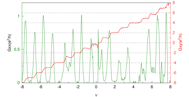
The Quantum Hall measurements at a perpendicular magnetic field of T were performed to estimate the value of capacitance and . Fig.S6 shows (green solid line) and (red solid line) versus the filling fraction () measured at a perpendicular magnetic field of T, establishing that both spin and valley degeneracies are lifted, indicating the high quality of the device.
S6 Comparision of Umklapp strength in the hBN moiré of BLG and SLG
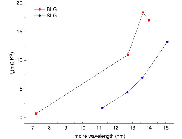
Fig.S7 plots the versus moiré wavelength for the hBN moiré devices, measured at . The Red data points are from our measured BLG-hBN moiré devices, and the blue data points of the SLG-hBN moiré devices from Ref [4]. As a similarity, both systems show the Umklapp scattering at .
However, there are significant differences between these two material systems (Fig.S7):
-
1.
The strength of is larger in BLG-hBN moiré than in the SLG-hBN moiré.
-
2.
depends non-monotonically on the moiré wavelength for BLG-hBN moiré, whereas for SLG-hBN moiré, increases monotonically with the moiré wavelength.
.
References
- Ashcroft and Mermin [1976] N. W. Ashcroft and N. D. Mermin, Solid State Physics (Holt-Saunders, 1976).
- Kaveh and Wiser [1984] M. Kaveh and N. Wiser, Electron-electron scattering in conducting materials, Advances in Physics 33, 257 (1984).
- Hideaki and Hidetoshi [1998] M. Hideaki and F. Hidetoshi, Electrical conductivity of interacting fermions. ii. effects of normal scattering processes in the presence of umklapp scattering processes, Journal of the Physical Society of Japan 67, 242 (1998).
- Wallbank et al. [2019] J. R. Wallbank, R. Krishna Kumar, M. Holwill, Z. Wang, G. H. Auton, J. Birkbeck, A. Mishchenko, L. A. Ponomarenko, K. Watanabe, T. Taniguchi, K. S. Novoselov, I. L. Aleiner, A. K. Geim, and V. I. Falko, Excess resistivity in graphene superlattices caused by umklapp electron-electron scattering, Nature Physics 15, 32 (2019).
- Moulsdale and Fal’ko [2023] C. Moulsdale and V. Fal’ko, Umklapp electron-electron scattering in bilayer graphene moiré superlattice, Phys. Rev. B 107, 144111 (2023).
- Ishizuka and Levitov [2022] H. Ishizuka and L. Levitov, Wide-range t2 resistivity and umklapp scattering in moiré graphene, New Journal of Physics 24, 052001 (2022).
- Bass et al. [1990] J. Bass, W. P. Pratt, and P. A. Schroeder, The temperature-dependent electrical resistivities of the alkali metals, Rev. Mod. Phys. 62, 645 (1990).
- Gasparov and Huguenin [1993] V. Gasparov and R. Huguenin, Electron-phonon, electron-electron and electron-surface scattering in metals from ballistic effects, Advances in Physics 42, 393 (1993).
- Messica et al. [1997] A. Messica, A. Soibel, U. Meirav, A. Stern, H. Shtrikman, V. Umansky, and D. Mahalu, Suppression of conductance in surface superlattices by temperature and electric field, Phys. Rev. Lett. 78, 705 (1997).
- Fisk et al. [1986] Z. Fisk, H. R. Ott, T. M. Rice, and J. L. Smith, Heavy-electron metals, Nature 320, 124 (1986).
- MacDonald et al. [1981] A. H. MacDonald, R. Taylor, and D. J. W. Geldart, Umklapp electron-electron scattering and the low-temperature electrical resistivity of the alkali metals, Phys. Rev. B 23, 2718 (1981).
- Behnia [2022] K. Behnia, On the origin and the amplitude of t-square resistivity in fermi liquids, Annalen der Physik 534, 2100588 (2022).
- Lin et al. [2015] X. Lin, B. Fauqué, and K. Behnia, Scalable resistivity in a small single-component fermi surface, Science 349, 945 (2015).
- Wang et al. [2020] J. Wang, J. Wu, T. Wang, Z. Xu, J. Wu, W. Hu, Z. Ren, S. Liu, K. Behnia, and X. Lin, T-square resistivity without umklapp scattering in dilute metallic bi2o2se, Nature Communications 11, 3846 (2020).
- van der Marel et al. [2011] D. van der Marel, J. L. M. van Mechelen, and I. I. Mazin, Common fermi-liquid origin of resistivity and superconductivity in -type srtio3, Phys. Rev. B 84, 205111 (2011).
- Ando et al. [2004] Y. Ando, S. Komiya, K. Segawa, S. Ono, and Y. Kurita, Electronic phase diagram of high- cuprate superconductors from a mapping of the in-plane resistivity curvature, Phys. Rev. Lett. 93, 267001 (2004).
- Maslov and Chubukov [2016] D. L. Maslov and A. V. Chubukov, Optical response of correlated electron systems, Reports on Progress in Physics 80, 026503 (2016).
- Trofimenkoff and Ekin [1971] P. N. Trofimenkoff and J. W. Ekin, Electron-phonon umklapp scattering processes in the low-temperature ultrasonic attenuation and electrical resistivity of potassium, Phys. Rev. B 4, 2392 (1971).
- [19] M. K. Jat, P. Tiwari, R. Bajaj, I. Shitut, S. Mandal, K. Watanabe, T. Taniguchi, H. R. Krishnamurthy, M. Jain, and A. Bid, Higher-order bragg gaps in the electronic band structure of bilayer graphene renormalized by recursive supermoiré potential. arXiv, 2023. arxiv:2304.01720 [cond-mat.mes-hall]. https://arxiv.org/abs/2304.01720. (accessed 2023-02-03).
- Ponomarenko et al. [2013] L. A. Ponomarenko, R. V. Gorbachev, G. L. Yu, D. C. Elias, R. Jalil, A. A. Patel, A. Mishchenko, A. S. Mayorov, C. R. Woods, J. R. Wallbank, M. Mucha-Kruczynski, B. A. Piot, M. Potemski, I. V. Grigorieva, K. S. Novoselov, F. Guinea, V. I. Fal’ko, and A. K. Geim, Cloning of dirac fermions in graphene superlattices, Nature 497, 594 (2013).
- Kuiri et al. [2021] M. Kuiri, S. K. Srivastav, S. Ray, K. Watanabe, T. Taniguchi, T. Das, and A. Das, Enhanced electron-phonon coupling in doubly aligned hexagonal boron nitride bilayer graphene heterostructure, Phys. Rev. B 103, 115419 (2021).
- Wang et al. [2019a] Z. Wang, Y. B. Wang, J. Yin, E. Tovari, Y. Yang, L. Lin, M. Holwill, J. Birkbeck, D. J. Perello, S. Xu, J. Zultak, R. V. Gorbachev, A. V. Kretinin, T. Taniguchi, K. Watanabe, S. V. Morozov, M. Andelkovic, S. P. Milovanovic, L. Covaci, F. M. Peeters, A. Mishchenko, A. K. Geim, K. S. Novoselov, V. I. Falko, A. Knothe, and C. R. Woods, Composite super-moire lattices in double-aligned graphene heterostructures, Science Advances 5, eaay8897 (2019a).
- Finney et al. [2019] N. R. Finney, M. Yankowitz, L. Muraleetharan, K. Watanabe, T. Taniguchi, C. R. Dean, and J. Hone, Tunable crystal symmetry in graphene-boron nitride heterostructures with coexisting moiré superlattices, Nature Nanotechnology 14, 1029 (2019).
- Yang et al. [2020] Y. Yang, J. Li, J. Yin, S. Xu, C. Mullan, T. Taniguchi, K. Watanabe, A. K. Geim, K. S. Novoselov, and A. Mishchenko, In situ manipulation of van der waals heterostructures for twistronics, Science Advances 6, eabd3655 (2020).
- Yankowitz et al. [2012] M. Yankowitz, J. Xue, D. Cormode, J. D. Sanchez-Yamagishi, K. Watanabe, T. Taniguchi, P. Jarillo-Herrero, P. Jacquod, and B. J. LeRoy, Emergence of superlattice dirac points in graphene on hexagonal boron nitride, Nature Physics 8, 382 (2012).
- Tiwari et al. [2023] P. Tiwari, D. Sahani, A. Chakraborty, K. Das, K. Watanabe, T. Taniguchi, A. Agarwal, and A. Bid, Observation of the time-reversal symmetric hall effect in graphene–wse2 heterostructures at room temperature, Nano Letters 23, 6792 (2023).
- Amin et al. [2022] K. R. Amin, R. Nagarajan, R. Pandit, and A. Bid, Multifractal conductance fluctuations in high-mobility graphene in the integer quantum hall regime, Phys. Rev. Lett. 129, 186802 (2022).
- Tiwari et al. [2022] P. Tiwari, M. K. Jat, A. Udupa, D. S. Narang, K. Watanabe, T. Taniguchi, D. Sen, and A. Bid, Experimental observation of spin-split energy dispersion in high-mobility single-layer graphene/wse2 heterostructures, npj 2D Materials and Applications 6, 68 (2022).
- Hofstadter [1976] D. R. Hofstadter, Energy levels and wave functions of bloch electrons in rational and irrational magnetic fields, Phys. Rev. B 14, 2239 (1976).
- Krishna Kumar et al. [2018] R. Krishna Kumar, A. Mishchenko, X. Chen, S. Pezzini, G. Auton, L. Ponomarenko, U. Zeitler, L. Eaves, V. Fal’ko, and A. Geim, High-order fractal states in graphene superlattices, Proceedings of the National Academy of Sciences 115, 5135 (2018).
- Huber et al. [2022] R. Huber, M.-N. Steffen, M. Drienovsky, A. Sandner, K. Watanabe, T. Taniguchi, D. Pfannkuche, D. Weiss, and J. Eroms, Band conductivity oscillations in a gate-tunable graphene superlattice, Nature Communications 13, 2856 (2022).
- Wang et al. [2019b] Z. Wang, Y. B. Wang, J. Yin, E. Tóvári, Y. Yang, L. Lin, M. Holwill, J. Birkbeck, D. J. Perello, S. Xu, J. Zultak, R. V. Gorbachev, A. V. Kretinin, T. Taniguchi, K. Watanabe, S. V. Morozov, M. Anđelković, S. P. Milovanović, L. Covaci, F. M. Peeters, A. Mishchenko, A. K. Geim, K. S. Novoselov, V. I. Falko, A. Knothe, and C. R. Woods, Composite super-moiré; lattices in double-aligned graphene heterostructures, Science Advances 5, eaay8897 (2019b).
- Nam et al. [2017] Y. Nam, D.-K. Ki, D. Soler-Delgado, and A. F. Morpurgo, Electron-hole collision limited transport in charge-neutral bilayer graphene, Nature Physics 13, 1207 (2017).
- Laitinen et al. [2015] A. Laitinen, M. Kumar, M. Oksanen, B. Plaçais, P. Virtanen, and P. Hakonen, Coupling between electrons and optical phonons in suspended bilayer graphene, Phys. Rev. B 91, 121414 (2015).
- Ochoa et al. [2011] H. Ochoa, E. V. Castro, M. I. Katsnelson, and F. Guinea, Temperature-dependent resistivity in bilayer graphene due to flexural phonons, Phys. Rev. B 83, 235416 (2011).
- Chen et al. [2008] J.-H. Chen, C. Jang, S. Adam, M. S. Fuhrer, E. D. Williams, and M. Ishigami, Charged-impurity scattering in graphene, Nature Physics 4, 377 (2008).
- Kashuba [2008] A. B. Kashuba, Conductivity of defectless graphene, Phys. Rev. B 78, 085415 (2008).
- Baber and Mott [1937] W. G. Baber and N. F. Mott, The contribution to the electrical resistance of metals from collisions between electrons, Proceedings of the Royal Society of London. Series A - Mathematical and Physical Sciences 158, 383 (1937).
- Xu et al. [2021] Y. Xu, F. Herman, V. Granata, D. Destraz, L. Das, J. Vonka, S. Gerber, J. Spring, M. Gibert, A. Schilling, X. Zhang, S. Li, R. Fittipaldi, M. H. Fischer, A. Vecchione, and J. Chang, Magnetotransport of dirty-limit van hove singularity quasiparticles, Communications Physics 4, 1 (2021).
- Hlubina [1996] R. Hlubina, Effect of impurities on the transport properties in the van hove scenario, Phys. Rev. B 53, 11344 (1996).
- Koshino [1960] S. Koshino, Scattering of Electrons by the Thermal Motion of Impurity Ions. II: , Progress of Theoretical Physics 24, 1049 (1960).
- Seiler et al. [2022] A. M. Seiler, F. R. Geisenhof, F. Winterer, K. Watanabe, T. Taniguchi, T. Xu, F. Zhang, and R. T. Weitz, Quantum cascade of correlated phases in trigonally warped bilayer graphene, Nature 608, 298 (2022).
- Jung et al. [2013] E. Jung, D. Park, and C.-S. Park, Zitterbewegung in bilayer graphene: Effects of trigonal warping and electric field, Phys. Rev. B 87, 115438 (2013).
- Tiwari et al. [2021] P. Tiwari, S. K. Srivastav, and A. Bid, Electric-field-tunable valley zeeman effect in bilayer graphene heterostructures: Realization of the spin-orbit valve effect, Phys. Rev. Lett. 126, 096801 (2021).
- Zhang et al. [2009] Y. Zhang, T.-T. Tang, C. Girit, Z. Hao, M. C. Martin, A. Zettl, M. F. Crommie, Y. R. Shen, and F. Wang, Direct observation of a widely tunable bandgap in bilayer graphene, Nature 459, 820 (2009).
- Icking et al. [2022] E. Icking, L. Banszerus, F. Wörtche, F. Volmer, P. Schmidt, C. Steiner, S. Engels, J. Hesselmann, M. Goldsche, K. Watanabe, T. Taniguchi, C. Volk, B. Beschoten, and C. Stampfer, Transport spectroscopy of ultraclean tunable band gaps in bilayer graphene, Advanced Electronic Materials 8, 2200510 (2022).
- Taychatanapat and Jarillo-Herrero [2010] T. Taychatanapat and P. Jarillo-Herrero, Electronic transport in dual-gated bilayer graphene at large displacement fields, Phys. Rev. Lett. 105, 166601 (2010).
- Zhu et al. [2022] Z. Zhu, S. Carr, Q. Ma, and E. Kaxiras, Electric field tunable layer polarization in graphene/boron-nitride twisted quadrilayer superlattices, Phys. Rev. B 106, 205134 (2022).
- He et al. [2020] Z. He, C. Yu, Q. Liu, X. Song, X. Gao, J. Guo, C. Zhou, S. Cai, and Z. Feng, High temperature rf performances of epitaxial bilayer graphene field-effect transistors on sic substrate, Carbon 164, 435 (2020).
- Uwanno et al. [2018] T. Uwanno, T. Taniguchi, K. Watanabe, and K. Nagashio, Electrically inert h-bn/bilayer graphene interface in all-two-dimensional heterostructure field effect transistors, ACS Applied Materials & Interfaces 10, 28780 (2018).
- Hasan et al. [2021] N. Hasan, U. Kansakar, E. Sherer, M. A. DeCoster, and A. D. Radadia, Ion-selective membrane-coated graphene-hexagonal boron nitride heterostructures for field-effect ion sensing, ACS Omega 6, 30281 (2021).
- Petrone et al. [2015] N. Petrone, T. Chari, I. Meric, L. Wang, K. L. Shepard, and J. Hone, Flexible graphene field-effect transistors encapsulated in hexagonal boron nitride, ACS Nano 9, 8953 (2015).
- Tang et al. [2013] S. Tang, H. Wang, Y. Zhang, A. Li, H. Xie, X. Liu, L. Liu, T. Li, F. Huang, X. Xie, and M. Jiang, Precisely aligned graphene grown on hexagonal boron nitride by catalyst free chemical vapor deposition, Scientific Reports 3, 2666 (2013).
- Wang et al. [2021] S. Wang, J. Crowther, H. Kageshima, H. Hibino, and Y. Taniyasu, Epitaxial intercalation growth of scalable hexagonal boron nitride/graphene bilayer moiré materials with highly convergent interlayer angles, ACS Nano 15, 14384 (2021).
- Summerfield et al. [2016] A. Summerfield, A. Davies, T. S. Cheng, V. V. Korolkov, Y. Cho, C. J. Mellor, C. T. Foxon, A. N. Khlobystov, K. Watanabe, T. Taniguchi, L. Eaves, S. V. Novikov, and P. H. Beton, Strain-engineered graphene grown on hexagonal boron nitride by molecular beam epitaxy, Scientific Reports 6, 22440 (2016).
- [56] A. L. Shilov, M. A. Kashchenko, P. A. Pantaleón, M. Kravtsov, A. Kudriashov, Z. Zhan, T. Taniguchi, K. Watanabe, S. Slizovskiy, K. S. Novoselov, V. I. Fal’ko, F. Guinea, and D. A. Bandurin., High-mobility compensated semimetals, orbital magnetization, and umklapp scattering in bilayer graphene moire superlattices. arXiv, 2023. arxiv:2311.05124 [cond-mat.mes-hall]. https://arxiv.org/abs/2311.05124. (accessed 2023-02-03).
- Sun et al. [2021] X. Sun, S. Zhang, Z. Liu, H. Zhu, J. Huang, K. Yuan, Z. Wang, K. Watanabe, T. Taniguchi, X. Li, M. Zhu, J. Mao, T. Yang, J. Kang, J. Liu, Y. Ye, Z. V. Han, and Z. Zhang, Correlated states in doubly-aligned hbn/graphene/hbn heterostructures, Nature Communications 12, 7196 (2021).
- Kumar et al. [2017] R. K. Kumar, X. Chen, G. H. Auton, A. Mishchenko, D. A. Bandurin, S. V. Morozov, Y. Cao, E. Khestanova, M. B. Shalom, A. V. Kretinin, K. S. Novoselov, L. Eaves, I. V. Grigorieva, L. A. Ponomarenko, V. I. Fal’ko, and A. K. Geim, High-temperature quantum oscillations caused by recurring bloch states in graphene superlattices, Science 357, 181 (2017).
- Hunt et al. [2013] B. Hunt, J. D. Sanchez-Yamagishi, A. F. Young, M. Yankowitz, B. J. LeRoy, K. Watanabe, T. Taniguchi, P. Moon, M. Koshino, P. Jarillo-Herrero, and R. C. Ashoori, Massive dirac fermions and hofstadter butterfly in a van der waals heterostructure, Science 340, 1427 (2013).
- Wang et al. [2019c] L. Wang, S. Zihlmann, M.-H. Liu, P. Makk, K. Watanabe, T. Taniguchi, A. Baumgartner, and C. Schönenberger, New generation of moiré superlattices in doubly aligned hbn/graphene/hbn heterostructures, Nano Letters 19, 2371 (2019c).