Spin-orbit coupling and Jahn-Teller effect in symmetry: an ab initio study on the substitutional nickel defect in diamond
Abstract
We analyze the spin-orbit and Jahn-Teller interactions in symmetry that are relevant for substitutional transition metal defects in semiconductors. We apply our theory to the substitutional nickel defect in diamond and compute the appropriate fine-leve structure and magneto-optical parameters by means of hybrid density functional theory. Our calculations confirm the intepretations of previous experimental findings that the 2.56-eV and 2.51-eV optical centres are associated with this defect. Our analysis of the electronic structure unravels possible mechanisms behind the observed optical transitions and the optically detected magnetic resonance signal, too.
I Introduction
Nickel is a typical contaminant in high-temperature high-pressure synthesized (HPHT) diamonds that paved the way to observe various nickel related optical signals in diamond in the past decades zaitsev2013optical ; Nadolinny2017review . However, various assignments of optical signals to defect structures were only tentative assumptions. Recent advances in the development of ab initio methods made it feasible to revisit the optical centres with high prediction power and identify the microscopic structure of the optical centres. As a recent example, we have identified the nickel-vacancy complex by means of advanced density functional theory (DFT) methods Thiering2021 as the origin of the 1.4-eV photo-luminescence (PL) centre Dean_1965 ; Collins1983 ; Kupriyanov_1999 which was previously associated with the positively charged nickel interstitial Isoya1990NIRIMg ; Paslovsky1992 ; Pawlik1998 ; larico2009electronic . Nickel-vacancy has symmetry where group theory analysis combined with DFT calculations showed the electron-phonon coupling within Jahn-Teller (JT) effect formalism intertwins with spin-orbit coupling, and the full complexity of the system should be considered to obtain the key magneto-optical parameters for identification of nickel-related optical centres Thiering2021 . In this paper, we apply this approach to the substitutional nickel defect (Ni) in diamond which has symmetry. Ni introduces orbitals to the electronic structure which presumably also a subject of spin-orbit coupling, and partial occupation of degenerate states could lead to JT effect. As we shall show below, a very general group theory analysis of degenerate orbitals in symmetry is required for understanding this type of defect systems.
The Ni configuration in diamond was observed in the electron paramagnetic resonance (EPR) spectra which is labelled as W8 LOUBSER1966firstW8 ; samoilovich1971electron ; Isoya1990W8 . After the discovery of W8 EPR centre LOUBSER1966firstW8 , the milestone experiments in the identification of Ni were (i) the fingerprint of isotope in the EPR spectrum with the hyperfine interaction between the electron spin and nuclear spin in isotopically enriched HPHT diamond samples samoilovich1971electron and (ii) observation of electron spin with hyperfine signals of four identical 13C nuclear spins Isoya1990W8 . The W8 EPR centre exhibits an isotropic tensor. These facts imply that the defect has symmetry. Furthmore, spin state indicates that it is a substitional defect in the negative charge state, i.e. Ni. This model was later confirmed by additional measurements and ab initio calculations Lowther1995 ; Larico2003 ; Larico2004 ; Larico2004basics ; Larico2004Err ; Chanier2013 . The ground state of Ni is well understood: Ni introduces a five times degenerate orbital of which level splits due to the tetrahedral crystal field of diamond as a triple degenerate one () lying in the fundamental band gap whereas the double degenerate orbital () is resonant with the valence band. The in-gap level is occupied by three electrons in the negative charge state which establishes the paramagnetic state. This electronic configuration is the orbital singlet multiplet state in symmetry.
The correlation between the Ni-related optical centres and the W8 EPR centre were studied either indirectly such as common appearance in the appropriate optical and EPR spectra with similar estimated concentrations or directly via optically detected magnetic resonance (ODMR).
In the former method, the correlation between the 1.883-eV and 2.51-eV Ni-related absorption centres and the W8 EPR centre was investigated. It was concluded that the 2.51-eV absorption centre is likely linked to the W8 EPR centre rather than the 1.883-eV absorption centre Collins1998W82.51correlate . Initial uniaxial stress measurements indicated that a triple degenerate state is involved in the 2.51-eV absorption spectrum Nazar1994T2T which was later revisited and concluded that optical transition is involved in the absorption process Nazar2001W82.51A1T2 , being consistent with the ground state of Ni. Although, the state is not optically allowed from ground state but it was assumed that spin-orbit coupling between the and makes this transition partially allowed. The shape of the first peak exhibit a doublet feature separated by 1.5 meV Nazar2001W82.51A1T2 . They interpreted this feature to the spin-orbit splitting of the state. Beside this feature a replica shows up at around 16.5 meV above the zero-phonon-line (ZPL) energy which is broadened compared to the shape of the ZPL emission Nazar2001W82.51A1T2 . The origin of the replica was not explained.
In the latter method, the 2.56-eV PL centre could be directly linked to the W8 EPR centre via ODMR measurements at cryogenic temperatures Pereira1994 ; Nazare1995 . Two individual features were observed in the ODMR spectrum excited by 325-nm laser in a 35-GHz microwave cavity Nazare1995 : (i) an electron spin resonance with the isotropic associated with the W8 EPR centre with producing a PL spectrum in the ODMR contrast which agrees well with the 2.56-eV PL spectrum in terms of the zero-phonon-line (ZPL) energy and the features in its phonon sideband; (ii) the hyperfine splitting originating from the nuclear spin in the P1 EPR centre, i.e. the neutral substitutional nitrogen donor, N with which produces a very broad gaussian-shape PL spectrum in the ODMR contrast. The ODMR contrast of the P1 centre was explained by a donor-acceptor pair (DAP) model, where the unknown acceptor interacts with the N donor as
| (1) |
where photon is emitted for which the energy depends the distance between the N and the acceptor , so it results in a broad fluorescence spectrum for the ensemble of DAPs. If the unknown acceptor is boron (acceptor level is at 0.37 eV above the valence band maximum, VBM) then the fluorescence spectrum can be well explained by taking the huge reconstruction energy of the N upon ionisation into account Nazare1995 . It was speculated that electron spin resonance of the acceptor in the ODMR spectrum was not observed because if the acceptor state is an effective-mass-like, then the degeneracy of the top of the VBM causing its EPR signal to be strongly strain broadened and difficult to detect, as in all cubic semiconductors Nazare1995 . Regarding the Ni-related ODMR feature, it is more difficult to come up with a unique model that explains the observation of the ground state EPR of Ni, in the luminescence. Nazaré et al. speculated Nazare1995 that one possibility is spin-dependent hole transfer from a distant acceptor to Ni, producing an excited luminescent state of Ni. We note that this may explain that the observed isotropic -factor in ODMR spectrum (2.0324) slightly differs from the -factor in the W8 EPR spectrum (2.0310) Nazare1995 . It is worth to note too that the 2.56-eV PL centre can be activated though a broad excitation at nm range ( eV) efficiently as performed by photo-luminescence excitation (PLE) measurements Lu2015 . This suggests that carriers trapping is indeed involved behind the ODMR process of Ni defect. We note that the reported negative ODMR contrast of the 2.56-eV PL in Ref. Pereira1994, was about in their experimental conditions (excitation wavelength of 365 nm applied in 36.2-GHz microwave cavity) which showed up as a positive contrast without reporting its magnitude in Ref. Nazare1995, in their experimental conditions (excitation wavelength of 325 nm applied in 35-GHz microwave cavity). This fact also implies that the ODMR process is not intrinsic to the Ni defect alone. Photo-EPR measurements were carried out in nickel doped diamonds and found that the intensity of W8 EPR signal decreases by photo-excitation with eV threshold energy which can be reinstated by photo-excitation with eV Pereira2003 .
II Methodology
We characterise Ni in diamond by plane wave supercell calculations within spin-polarised DFT as implemented in the vasp 5.4.1 code Kresse:PRB1996 . We determine the electronic structure within the Born-Oppenheimer approximation where the ions are treated as classical particles. We relaxed the atomic positions until the forces acting on the ions fall below 10-2 eV/Å. We embed the defect in a 512-atom diamond supercell and we sample the Brillouin-zone at the -point. We used the projector-augmentation-wave-method (PAW) Blochl:PRB1994 ; Blochl:PRB2000 as implemented in vasp. We used the standard PAW projector for carbon and Ni_pv PAW projector for nickel that includes the atomic orbitals as valence. We applied a plane wave cut-off energy at 370 eV for the plane wave basis that was already proven to be convergent for SiV defect and many other defect system in diamond Gali:PRB2013 ; Thiering2015 ; thiering2018theory ; Thiering2021 ; Thiering2017SOC ; Thiering2016 ; thiering2018emph . We calculate the excited states with the constrained-occupation DFT method or SCF method Gali2009 . We employed the Heyd-Scuseria-Ernzerhof (HSE06) hybrid functional Heyd03 ; Krukau06 which reproduces the experimental band gap and the charge transition levels in diamond or other group-IV semiconductors within 0.1 eV accuracy Deak:PRB2010 ; Gali2009 . For the charged supercell we applied the Freysoldt-Neugebauer-van de Walle correction to the total energy Freysoldt2009 . We use our home-built code to compute the electron-phonon spectrum of the Jahn-Teller modells that we successfully applied to other systems too Thiering2017SOC ; thiering2018emph .
III Results
We combine group theory description of the Ni defect with DFT calculations. We start with the calculated electronic structure and charge transition levels of the defect. We identify the most common charge states under typical experimental conditions in this section. We continue with the detailed discussion of the ground state manifolds of the most relevant charged states of the defect and then we describe the optically accessible excited states. Finally, we discuss our findings in the light of the observed 2.51-eV absorption centre and the 2.56-eV PL centre including the possible mechanisms behind the ODMR signature.
III.1 Electronic structure of Ni
The Ni atom introduces orbitals which splits to double degenerate orbitals and triple degenerate orbitals in the tetrahedral crystal field of diamond. In the defect molecule diagram, these orbitals and the orbitals interact with the four dangling bonds of the neighbour carbon atoms that results in and molecular orbitals under symmetry. The and orbitals can form bonding and anti-bonding molecular orbitals lying deep in the valence band and high in the conduction band, respectively. The orbitals do not recombine with the dangling bonds and they remain atomic like. The level of orbitals is resonant with the valence band in the neutral charge state of the defect as plotted in Fig. 1(a). Finally, the representations of the orbitals and the dangling bonds again form bonding and antibonding molecular orbitals. The bonding combination falls deep in the valence band whereas the antibonding combination appears in the gap. In the context, we call this antibonding orbital simply the state in the gap which is responsible for the ground state manifolds of the Ni defect. In the optical excitation, the atomic like states may play a role. The calculated Kohn-Sham states are depicted in Fig. 1(b).
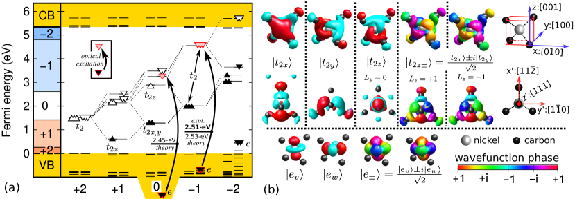
According to this defect molecule analysis, the defect has the electronic configuration, where is the charge state of the defect. As the triple degenerate may accommodate six electrons, the possible charge states may go from the to . We calculated the total energies of the corresponding charge states () and calculated the adiabatic charge transition levels as , where is the calculated VBM energy and now it is aligned to zero in Fig. 1(a).
We find that the aniticipated and states are not stable at all, and the and charge states are marginally stable as a function of the Fermi-level in diamond. Therefore, we do not analyze the and charge states further. The calculated level is at about eV, which means that it is about eV, where is the energy of the conduction band minimum (CBM). In other words, if the defect was in the neutral charge state then about 2.6 eV photo-excitation energy is required to ionise to charge state, and if the defect was in the charge state then about eV photo-excitation energy is required to re-ionise it back to the neutral charge state. Ni can be readily ionised to the neutral charge state by the photo-excitation threshold energy at about 1.5 eV. It can be read out from Fig. 1(a) that Ni may be stable in -type diamond and near-infrared photo-excitation is needed below the photo-ionisation threshold energy in order to observe its absorption or fluorescence signal. In practice, these conditions are not fulfilled, thus we will only briefly discuss the ground state of Ni. We rather focus our discussion to the negatively charged and neutral Ni defects.
We briefly discuss now the 2.51-eV absorption and 2.56-eV PL centres in the light of the calculated photo-ionisation threshold energies. According to the calculated level at around eV, both optical centres might correspond to the neutral excitation of both Ni and Ni defects. The 2.56-eV PL centre has the ZPL energy just below the calculated NiNi ionisation threshold energy. Thus, the calculated ionisation threshold energies could not distinguish alone which optical centre belongs to which defect charge state. In order to identify these optical centres, we analyze the ground and excited states of Ni and Ni in detail in the next sections.
It is intriguing that the 2.56-eV emission can be observed above-band-gap excitations Lu2015 , and its ODMR signals were observed by 325-nm (3.81-eV) photo-excitation Nazare1995 and 365-nm (3.40-eV) photo-excitation Pereira1994 experiments. In the latter two experiments, the photo-excitation energies are both above the ionisation threshold energies for both the NiNi and NiNi processes, where the electron is promoted from the valence band to the empty defect level and from the occupied defect level to the conduction band, respectively. The calculated level at around eV implies that the electron is promoted from a deeper energy region of the valence band in the first process rather than it is excited from the occupied defect level to little above the conduction band minimum in the second process. As the electron density of states rapidly increases going farther from the band edges this implies that NiNi process is much more efficient than NiNi process. As a conseuqence, the ultraviolet excitation will stabilise the Ni charge state, so the defect stays much longer time in the charge state than in the charge state.
III.2 Ground state of Ni
It is likely that ultraviolet photo-excitation stabilises the negative charge state of Ni, and the totally filled electronic configuration of Ni can be readily analyzed as a basis for the more complex electronic configurations. Therefore, we start the analysis with the ground state electronic structure of Ni.
According to first Hund’s rule the three electrons in the triple degenerate orbitals will form a high-spin electronic configuration. The wavefunction of such quartet state can be expressed as
| (2) |
where we define the three particle () symmetrisation
| (3) |
and () anti-symmetrisation
| (4) | |||
operators for the sake of simplicity. In addition, we use shortened notation to label orbitals in the context from now on. Our results are in agreement with previous ab initio studies Larico2004basics ; Chanier2013 , the ground state is a multiplet. The spin of W8 EPR centre emerges from the three unpaired electrons fillling the orbitals in Ni.
III.3 Shelving doublet states of electronic configurations in Ni
It is clear that electronic configuration can form doublet states too as the total number of possible combinations of muliplet states is where quartet state produces only four multiplet states from them. The other configurations form doublet manifolds that should be expressed as a combination of Slater-determinants. First, we determine the possible configurations with single Slater-determinants. There are 8 possible occupations where we pin electrons on individual spin-orbitals as
| (5) |
where combinations and the totally symmetric combinations are reserved for the ground state as
| (6) |
that is equivalent to Eq. (2). Therefore, the remaining four-dimensional subspace spans a state as
| (7) |
By constraint occupation of the Kohn-Sham orbitals, the total energy of the system can be calculated by spin-polarised HSE06 functional as given in Eq. (5). The exchange-correlation functional of HSE06 may not be able to capture the high correlation which can be described as combinations of Slater-determinants and the resulting solutions will be not the true eigenstate of the doublet spin state.
With this caveat, we carried out ab initio calculations for the single Slater-determinant configuration, e.g. of the Kohn-Sham states which yields 0.35 eV with respect to the calculated total energy of state. This was achieved by restricting the symmetry to symmetry. By enabling the symmetry reduction for the electronic configuration, the energy gain has become negligible at 1.4 meV. We conclude that there will be no Jahn-Teller effect for the doublet configurations in the first order. The determinant is an 33% admixture of and 66% of multiplets, thus we expect the level of lying above that of by roughly 0.35 eV.
Other possible configurations are
| (8) |
which reduces into a spin doublet as
| (9) |
and an another spin doublet as
| (10) |
We expect that the levels of these states lie above those of the maximally open shell configurations’ doublets because the Coloumb repulsion is not compensated by exchange interaction in the former. In Kohn-Sham DFT method, we could calculate one of the single Slater-determinants electronic configuration as expressed in Eq. (8). Their total energy exceeds that of by about 0.5 eV within symmetry.
Finally, we conclude based on the Coulombic repulsion principle that has the highest total energy among the considered doublet manifolds as it exhibits the most symmetric polynomial, that is, , in contrast to with .
III.4 electronic configurations in Ni
The ground state manifolds of Ni exhibit electronic configurations in symmetry which may be a subject of Jahn-Teller effect and spin-orbit coupling. The total number of manifolds is . According to direct product tables atkins1970tables of point group, there are four multiplets that can be read as
| (11) |
where we kept the fermionic anti-symmetric property of the wavefunctions, thus combinations do not occur. Next, we show the symmetrically adapted wavefunctions. According to our ab initio results the ground state of is a that reads as
| (12) |
It is followed by the singlet state which can be expressed as
| (13) |
where we interchanged the two-particle anti-symmetrisation and symmetrisation operators on the spin and orbital part of the wavefunctions.
The triplet configuration can be determined by Kohn-Sham DFT as a configuration. We note that triplet is Jahn-Teller unstable. We obtained 159 meV relaxation energy when we removed the symmetry constraint during the geometry optimization. We obtained 47 meV higher total energy for the with symmetry restriction that gained 125 meV relaxation energy upon removal the symmetry constraint. We note that the configuration is the 50%-50% admixture of the and multiplets, thus our results can be interpreted as that the singlets are above the triplet by about 47 meV.
Eqs. (12) and (13) span a dimensional open-shell subspace where the electrons are placed to different orbitals within orbitals. Next, we discuss the case of the closed shell configurations (, , ) which leads to the and multiplets which may read as
| (14) |
and
| (15) |
respectively. We note that and are multi-configurational states, thus Kohn-Sham DFT may not provide good estimates for their total energies. Nevertheless, we can determine the total energy within spin-averaged Kohn-Sham DFT calculation for the individual (, , ) configurations that forces the same orbitals in each spin channel. According to our results, the total energy of the closed shell configurations lies above that of the ground state by 0.70 eV within symmetry. After removing the symmetry constraint in the geometry optimization procedure, the calculated energy difference is reduced to 0.18 eV that shows a giant 0.52 eV Jahn-Teller energy. This effect might suppress the electronic correlation energy between and , similarly to the product Jahn-Teller effect in SiV0 defect of diamond Thiering2019prodJT ; Harris2019 . In the next section, we discuss the Jahn-Teller effect in detail for electronic configuration in symmetry.
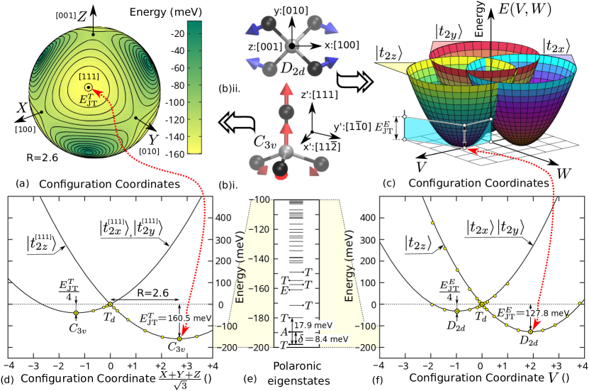
III.4.1 Jahn-Teller effect in Ni
The theory of Jahn-Teller interaction in symmetry was already discussed in the literature (see Ref. bersuker2013jahn, and references therein). We apply this theory to the Ni defect. The symmetry is dynamically distorted by and vibration modes, i.e. vibronic system. With assuming an effective vibration and an effective vibration, the vibronic system may read as
| (16) |
where operators depict the geometry distortion from the vibration mode governed by while depict to that of vibration mode governed by . and electron-vibration coupling parameters can be determined bersuker2013jahn as
| (17) |
where the is the Jahn-Teller energy and is the respective effective phonon and frequencies. The global minima in the five-fold configurational space are either one of the 3 equivalent tetragonal extrema with symmetry or 4 equivalent trigonal extrema with symmetry. The actual global energy minima, whether tetragonal or trigonal, depend on the properties of the given system. As the and vibrations are orthogonal each other and they lead to trigonal and tetragonal distortions, there individual contributions can be determined by DFT calculations as
| (18a) | |||
| (18b) | |||
where total energies are obtained from HSE06 DFT calculations with geometry optimization under the point group. We determined by mapping the parabolicity of the adiabatic potential energy surface along the and normal coordinates.
We solved the JT problem up to 8-phonon limit by substituting our ab initio parameters meV, meV, meV, meV into Eqs. (17) and (16). In accordance to previous results bersuker2013jahn , the lowermost eigenvalue of the electron-vibration or vibronic system is a triple degenerate level which is followed by an level by 9.0 meV. also experience spin-orbit effect as the maximum degeneracy in the double group is four-fold. In the next section, we study the spin-orbit interaction of this state.
III.4.2 Spin-orbit fine structure of Ni
We introduce the spin-orbit operator as follows. The operators depict an effective orbital moment within the orbitals. One may note that there are two electrons in the orbital, thus
| (19) |
where
| (20) |
and ’s are regular spin operators for a given spin multiplicity. For the triplet spin of Ni, we use
| (21) |
The complex unit in emphasizes that the orbitals lose their real-value character when spin-orbit interaction is considered unlike the case of electron-phonon interaction, e.g. Eq. (16)). For example, if the quantisation axis is along the ”z” [001] axis then the eigenfunctions are and that we visualize in Fig. 1(b).
We determined the bare intrinsic spin-orbit strength at single particle level by ab initio calculations: meV. The single particle operator can be depicted by the same matrices that of Eq. (20) in contrast to a single electron’s spin that can be depicted by two-times-two Pauli matrices: . We note that acts only between single particle levels but Ni is effectively a two-electron system, see Eq. (12). Therefore, the spin-orbit strength for the two-particle system will be . In order to solve the previous equation, we introduce an Clebsch-Gordan coefficient for because only posseses both angular and spin moments, so exhibiting remains intact from spin-orbit coupling.
However, the intrinsic value of spin-orbit coupling is reduced by the Ham reduction factor. That is, the orbital operators are mediated by strong Jahn-Teller renormalization thus are subject to the so called Ham reduction factors (see section 5.6 about reduction factors in Ref. bersuker2013jahn, for details). In other words, the triply degenerate phonons can entangle the three , orbital characters. That is the ground state that can be depicted in a Born-Oppenheimer basis by ladder operators acting on vibration modes: , where we depicted only the first terms in the series expansion. Therefore the electron-phonon entangled will exhibit a reduced spin-orbit strength as the ground state is not a pure electronic character anymore: mixes in. The intrinsic orbital angular momentum will be partially quenched by the factor: . Thus the observable spin-orbit coupling will be partially quenched too: . We report the reduction factor as by means of Eq. (16) when we capped the phonon quanta as . Finally, the acting for ’s orbital and spin moments will be
| (22) |
where meV. Our positive is in agreement with Hund’s rules: the lowermost state in a () singlet followed by () at energy and () at , where we depicted double group representations koster1963properties for the symmetry in parentheses. However, higher order spin-orbit terms may dominate over the linear similarly to that of Ni’s excited state that we will describe in Eq. (29) in the next section.
III.5 Optically excited states of Ni
We turn to the interpretation of the optical spectra of Ni-related centres. First, we consider the optically allowed excited states of Ni. To this end, one has to go beyond multiplets because no other quartet state can be formed than the ground state. As can be seen in Fig. 1(a), a resonant state occurs in the valence band from which an electron may be promoted to the empty state in the spin minority channel. This results in electron configuration which is equivalent to hole configuration. We assume that the prefers the multiplet. With this constraint, the configuration reads as
| (23) |
According to Hund’s first rule, we expect that the high-spin quartet states are more stable than the low-spin doublet states. We focus now on the discussion of the optically allowed quartet states. In the construction of the quartet states in Eq. (23) we may start with the doublet state which can be expressed by (; ) quadratic polinomials. These polynomials are represented by the and Ni atomic orbitals as depicted in Fig. 1(b). The lowest order polynomial for triple degenerate representation under point group is linear. As a consequence, the quartet states should transform as fourth order polynomials. By applying projection operators in group theory one finds that { ; ; } belongs to the irreducible representation whereas { ; ; } belongs to the representation. These states may be expressed by using and as
| (24) |
and
| (25) |
It may be recognized that states can be constructed by swapping and in the multiplets of states. Another important and surprising observation is that both and states may be described as a single Slater-determinant (see the last row in Eqs. (24) and (25)). As a consequence, the total energy of and states can be principally estimated from KS DFT SCF method once the respective and electronic configurations could be converged in this procedure. We obtained 2.61 eV and 2.95 eV excitation energies w.r.t. the ground state’s energy within symmetry.
The electronic configurations and their energy levels may then be expressed by omitting the spin degrees of freedom as follows,
| (26) |
where we define the and projectors as
| (27a) | |||
| and | |||
| (27b) | |||
However, we learnt from the of Ni that is a subject to JT effect. Since and inherit this electron configuration one can suspect that JT effect is not negligible in and states of Ni. Indeed, 84 meV energy is released once we removed the symmetry constraint in our ab initio calculations during the SCF procedure. In the next section, we study the JT effect in the and states with using and projectors in Eqs. (27a) and (27b).
III.5.1 Jahn-Teller effect
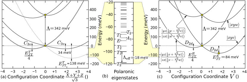
We already analysed the JT effect for the system in Sec. III.4.1. We rely on this analysis which becomes more complex with taking both and states that might also interact with each other through electron-phonon coupling that we describe by JT effect. This may be described as
| (28) |
where we assume that should not depend on and orbitals. That is, in Eq. (28) is the dot product of from Eq. (16) with a 22 unit matrix to span the six dimensional degrees of freedom from the orbitals. In the derivation, we used the lemma which leads to diagonal and offdiagonal terms where we can distribute the JT interaction acting on inside the manifolds (diagonal terms) or induce orbital excitation between the multiplets. As a consequence, JT interaction induces mixing of electronic characters.
First, one may check that the ”” vibration modes do not lead to this kind of orbital mixing that we depicted in Eq. (28). That is, Eqs. (27a) and (27b) show that the projectors are diagonal at their bottom-right edges, i.e. , , respectively. This bottom-right edge is influenced only by the diagonal matrix element from Eq. (16) and thus does not inflict any interaction between and configurations of and multiplets, respectively. One may argue that the upper two 22 matrix blocks in Eq. (27) are not diagonal. However, these matrix blocks can be diagonalized with , orbital rotations. Therefore, offdiagonal terms in Eq. (28) do not appear for -type distortions. Therefore, APES remains the same for states. They are just shifted by electronic splitting of Eq. (26) and thus Eq. (18b) can be used to determine strength. According to our ab initio calculations, the JT distortion energy is meV mediated by meV vibrations.
However, in Eq. (18a) is effective in this regard. , , in Eq. (16) are purely offdiagonals that can create cross-talks between 22 blocks of the projectors in Eq. (27) and thus mix the electronic characters since the three 22 blocks are not diagonal in the same basis. As we saw in the previous paragraph, the third block is diagonal in basis but the first two blocks are diagonal only in , thus will cause orbital excitation between multiplets. In other words, the APES will not be just a shifted replicas that of ’s JT APES depicted in Sec. III.4.1. Indeed, we report that the distortion energy is severely quenched for ””-type distortions: meV (that was 160 meV for ) that demonstrates that Eq. (17) should not be directly employed for ’s excited states. Therefore we used meV and meV that of that resembles this excited state. Both configurations confine four electrons in orbitals thus we expect similar JT instability for these two cases approximately. We also assume that the pure atomic orbitals in states do not affect the Jahn-Teller instability too much.
Therefore, we take an exact diagonalisation of Eq. (28) in order to approximate the vibronic levels up to phonon limit. By considering the offdiagonal terms, the and can be entangled by phonons which will ultimately lead to a vibronically strongly coupled lowermost polaronic state quickly followed by an additional state at meV. We observe that at any choice for below meV the effective energy spacing will be strongly quenched as by the Ham reduction factor. We note that affects orbital operators transforming as representation of symmetry (see section 5.6 about reduction factors in Ref. bersuker2013jahn, for details). In our present case, energy exhibits the same order of magnitude that of or thus the two effects will compete with each other. As a consequence, will be dependent on thus it is in our case.
III.5.2 Spin-orbit fine structure
We learnt from ground state of Ni that spin-orbit interaction occurs. Nazaré et al. was able to fit the following spin-orbit Hamiltonian (see Eq. (2) in Ref. Nazar2001W82.51A1T2, ) to the fine structure of the 2.51-eV absorption centre,
| (29) |
where the orbital operators are that of Eq. (20) and spin operators are extended for quartet () multiplicity to depict the spin-orbit interaction similar way to that of Eq. (19) for Ni. However, in contrast to that of Eq. (19), Eq. (29) is an effective Hamiltonian in which the orbital operators are mediated by strong Jahn-Teller renormalization, i.e. those are subject to the so-called Ham reduction factors. In this case, the reduction factor is because our three orbital operators transform as the representation. Therefore, the intrinsic orbital angular momentum will be partially quenched by the factor: thus the observable spin-orbit coupling will be partially quenched too, i.e. . We report the reduction factor as by means of Eq. (28) with using for the expression of polaronic states.
The spin-orbit coupling parameter should be also determined. We were not able to converge the excited state together with spin-orbit coupling, thus we determined by taking the value of Ni that bears the same number of electrons on its orbital: meV. We note that , strictly speaking, acts only on single particle KS levels. Therefore, we introduce an additional Clebsch-Gordan coefficient for : . That is, in other words, neither or possesses angular momenta, thus only couples with its moment and spin. In summary, we report as meV that is surprisingly near the experimentally observed meV measured in the 2.51-eV absorption centre by Nazaré et al. in Ref. Nazar2001W82.51A1T2, .
However, our current level of theory was not able to determine the additional higher order and parameters in Eq. (29)). That is, determining those coefficients requires second order effects that would utilize , , spin doublet states and even the ground state through flipping terms. We report meV from ab initio calculations that would scale the parameters by means of second order perturbation theory as
| (30) |
with assuming a heuristic 1 eV electronic splitting. Our result in Eq. (30) is in the same order of magnitude that was reported in Ref. Nazar2001W82.51A1T2, as meV, meV further supporting the association of 2.51-eV absorption centre to the optical transition of Ni.
III.6 Excited states of Ni
We continue the investigation with the excited states of electronic configuration which could be either or spin configurations coupled to which is a hole left on the orbital with symmetry with either or spin state. We start the analysis with the case which reads as
| (31) |
The is the case when the spin from and the spin from the hole is coupled by the opposite spin states. The maximally spin-polarised wavefunctions are the followings,
| (32) |
where the can be either or . We note that the single Slater-determinant dominates () the wavefunction, thus we expect that its total energy can be well estimated by SCF DFT method which results in 2.61 eV excitation energy within symmetry. The JT energy is negligibly small (3 meV). The total energy of the state should be accurate by SCF DFT method as a single Slater-determinant, and it yields 2.08 eV excitation energy. The JT energy is again tiny (5 meV) as expected.
We now turn to the other manifolds based on electronic configurations which result in , and multiplets. We already proved during the discussion of Ni that multiplet exhibits the lowest total energy. Therefore, we only focus to that manifold as it is combined with a hole left on the orbital with symmetry which reads as follows
| (33) |
We assume again that the singlet manifolds lie at higher energies than the triplet manifolds. We express the maximal spin states of the optically allowed triplet manifolds,
| (34) |
where the other spin states can be readily obtained and explicitly given here. It can be observed that these states are highly correlated. The largest determinant contribution is prefactors to where the SCF DFT results can converge to
| (35) |
As a consequence, the total energies of these individual triplet states cannot be well determined by SCF calculations. Nevertheless, we calculated the SCF total energy of Eq. (35). We obtain 2.45 eV excitation energy within symmetry. The calculated JT energy is 43 meV which is expected due to the partially filled orbitals. As the direct calculation of these states is not feasible with DFT methods, we do not analyze these states further but we give a very rough estimate for their ZPL energies at around 2.4 eV.
III.7 Ground state of Ni
We briefly discuss paramagnetic Ni which may be observed in special p-type doped diamond sample. Ni exhibits electronic configuration which yields multiplet. This is a subject to JT effect and spin-orbit interaction.
We can apply JT theory as given in Eqs. (16) and (17) which results in meV, meV and meV, meV. These results imply that the Ham reduction factor is significant that may act on the spin-orbit energy gaps. We determined up to the 8-phonon limit. We determined the spin-orbit coupling as 8.6 meV. We note here that no Clebsch-Gordan coefficient is needed in this case since the multiplet can be described as a single orbital. Therefore, the spin-orbit coupling will lead to an followed by an high moment state with meV. We again note that higher order spin-orbit terms may appear similarly to that of Eq. (29).
IV Discussion
We summarise the calculated excitation energies and photo-ionisation threshold energies of Ni defects in diamond in Fig. 4. As we can see the neutral and negatively charged Ni has photo-ionisation energies and excitation energies are close to 2.5-2.7 eV, thus one has to study the nature of optical excitations in great detail. This includes the vibronic states and levels as well as the spin-orbit couplings and fine structure levels (see Fig. 4). These results are the base for the discussion of the origin of 2.51-eV absorption centre and 2.56-eV ODMR centre. We note that the 2.5 eV and 3.0 eV threshold energies in the photo-EPR measurements Pereira2003 as the de-activation and re-activation of the W8 EPR centre associated with the ground state of Ni cannot be explained by simple ionisation and re-ionisation processes of Ni, according to our results. In particular, we show below multiple evidences that the 2.51-eV absorption centre is associated with Ni, thus the photo-ionisation threshold energy towards the conduction band minimum cannot be smaller than 2.51 eV. It is rather likely that carriers trapping is also involved in the process where the carriers might be generated by photo-ionisation of other defects in that diamond sample.
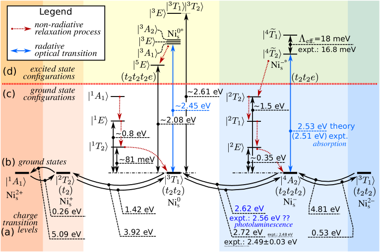
IV.1 The 2.51-eV absorption centre and Ni
We reiterate here that the 2.51-eV absorption centre is associated with a optical transition according to the last observations which shows a replica at 16.5 meV above the ZPL feature Nazar2001W82.51A1T2 . Both the ZPL and the replica show a fine structure with about 1.5 meV splitting where the ZPL’s fine structure is depicted by Eq. (29)’s effective spin-orbital Hamiltonian. The Ni has orbital ground state whereas Ni has the appropriate ground state, thus we analyse the excited state of Ni as the possible candidate for the 2.51-eV absorption center. Indeed, the calculated ZPL energy is at 2.53 eV, close to the experimental one. Additionally, we were able to predict the experimentally observed SOC parameter meV as meV suggesting that the model in Ref. Nazar2001W82.51A1T2, is correct.
We found that the lowest energy quartet excited state is indeed for Ni which is optically forbidden in the first order, see Fig. 3(b). The next quartet state is a separated by about 18.02 meV from the state that is very close to the observed replica at 16.5 meV. We emphasize that this effect is very similar that we found for the neutral silicon-vacancy center in diamond Thiering2019prodJT where two polaronically entangled states lie close to each other in the Jahn-Teller solution. An additional analog to the properties of the neutral silicon-vacancy optical centre in diamond is that the first state is an optically forbidden which is quickly followed by the optically allowed by meV that is an order of magnitude smaller than that of the vibration mode’s energy ( eV). A similar situation is apparent for Ni: . Therefore, the vibration replica is significantly broader ( meV, see Fig. 1 in Ref. Nazar2001W82.51A1T2, ) than that of the ZPL ( meV) but not as broad as that of a real first phonon vibronic replica ( meV) of Huang-Rhys theory Alkauskas:NJP2014 ; Thiering2017SOC . Therefore, we argue that the 16.8-meV splitting is a fingerprint of the Jahn-Teller instability.
The optical activity of the dark state may be explained by the JT coupling to the bright multiplet which brings a character to the state of about 5% due to offdiagonal terms in Eq. (28). The remaining 95% of ’s optical transition dipole moment would be still active around (435 nm). However, this peak may be not recognized because it is simply obscured by the phonon sideband of the 2.51-eV peak and overlapping with the photo-ionisation threshold at about 2.72 eV converting Ni to Ni. Unfortunately, absorption data beyond eV ( nm) is not reported for the 2.51-eV centre, to our best knowledge, to gain insight about this issue.
Next, we discuss the strength of the ZPL and the replica. First, we note that even the ZPL of the lowermost only contains 7% contribution and 1% Debye-Waller factor, thus only 1% optical transition dipole moment is visible in the replica of 2.51 eV. Additionally, the spin-orbit coupling may turn optically allowed by amount.
The missing fluorescence of the 2.51-eV band may be explained by the fact that the optical transition dipole moment is weak and , and doublets exist between the 2.51-eV optical transition that could lead to an efficient non-radiative channel for the excited state. The estimated spin-orbit coupling between the and states is about meV which mediates the intersystem crossing in the non-radiative process.
IV.2 The 2.56-eV ODMR centre and Ni
The 2.56-eV ODMR centre is associated with the ground state of Ni but observed in luminescence which may be explained by the optical emission from Ni as speculated in Ref. Nazare1995, . We discuss this scenario in the light of our results. One of the excited states could be calculated with relatively high accuracy at 2.61 eV which is resonant with the calculated photo-ionisation threshold energy at 2.62 eV. The excitation energy of the other three triplet excited states could not well calculated by SCF method and it might fall below the photo-ionisation threshold. However, the strength of optical transition associated with at Kohn-Sham orbital level is very weak because the state is well localised on Ni orbitals. We think that it is unlikely that those states are involved in the ODMR signal. We here sketch another scenario.
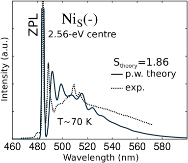
As we discussed in Sec. III.1, Ni spends in the negative charge state upon ultraviolet illumination according to our calculations, and ultraviolet illumination also releases holes in diamond samples Nazare1995 . Ni can trap holes with very high hole capture rates that results in bound exciton states of Ni. We note that ODMR signal via bound exciton excited states have been observed for the neutral silicon-vacancy defect Zhang2021 , and it was argued for nitrogen-vacancy centre that bound exciton states have giant hole capture cross section Lozovoi2021 . We analysed the bound exciton states for silicon-vacancy centre in symmetry Zhang2021 . For Ni plus hole system, we should consider symmetry as the Ni ground state electronic configuration is stable in symmetry and the hole split from valence band maximum should have negligible JT effect. For the hole state, we may use the effective mass theory as explained in Ref. Zhang2021, . The lowest energy state transforms by symmetry which has an type envelope function. The effective mass state is relatively well localised around the core of the defect for which the optical transition dipole moment is relatively strong. The phonon sideband of the fluorescence spectrum may be well estimated by the optimized geometries of the Ni representing the excited state and Ni for the ground state within Franck-Condon approximation. Indeed, the calculated and observed PL spectra agree well (see Fig. 5). We conclude that the 2.56-eV PL and ODMR signals are associated with the bound exciton emission of Ni.
Understanding the ODMR contrast requires the analysis of the fine structure of the ground state and the excited state. The ground state is which splits to () state, () state and () states in ascending energy order where we label here the double group representations. The splitting is caused by the spin-orbit interaction which is roughly estimated to be at 0.12 meV based on our ab initio calculations that do not contain quadratic spin-orbit contributions that might be also significant. Nevertheless, we assume that the order of these levels retains. In this case, the ground state has no effective coupling to the external magnetic field in the ground state, thus it may be not observable in EPR measurements. The Jahn-Teller nature of the ground state could also make challenging to observe the triplet state in EPR experiments. In the excited state, the electronic configuration has spin state which is combined with a hole in the valence band maximum with state (). The composed system transforms at which again results in state, state and states split by spin-orbit interaction, where here. The initial population of the excited state branch may depend on the applied external magnetic field, temperature and strain in the sample. The final strength and sign of the ODMR contrast will depend on the population of these states in the excited state manifold. Further analysis of this process and the -factor of the state is out of the scope of the present study.
IV.3 Interaction of nickel defects with other defects in diamond
In the previous sections we already outlined that defect-defect interactions play a crucial role in the manifestation of the ODMR signal associated with the substitutional nickel defect in diamond. Since the ionisation energies of defects are much larger than the operation temperatures (typically, room temperature) the exchange of carriers are mediated by photo-excitation. The nitrogen donor can be efficiently activated by photo-excitation energy at 2.1 eV and above. The optical signals of substitional nickel defects have ZPL energies at 2.51 eV and above, thus surrounding nitrogen donors around the nickel defects provide electrons towards the nickel defects upon illumination which may stabilise their negative charge state. On the other hand, if nickel-vacancy (NiV) defects are also present in the sample then this illumination results in ejecting holes by converting the 1.4-eV PL centre (negatively charged NiV defect) to doubly negative charged NiV defects (see Ref. Thiering2021 ). Thus, the ratio and location of the nitrogen and NiV defects with respect to the substitutional nickel defects can be decisive about the magneto-optical fingerprints of the substitional nickel defects. If vacancies or vacancy aggregates are also present in diamond, e.g. after implantion, then they also enter as traps for holes (in their negative charge states) and as sources of holes upon illumination of neutral vacancies or vacancy clusters. The latter can indeed occur as the calculated acceptor level of the vacancy or divacancy with respect to VBM is lower than 2.5 eV Deak2014 . These defects and possibly boron acceptors are the major players in the photodynamics of the substitional nickel defect in diamond.
V Summary
We studied the electronic structure of the Ni transition metal substitutional defect with symmetry by means of group theory analysis and plane wave supercell density functional theory calculations. We find that the negative and neutral charge states are the most relevant configurations for the substitutional Ni defect in diamond. We observed strong electron-phonon coupling and spin-orbit coupling in certain states of the defect. We compared the ab initio results with the previously reported 2.51-eV absorption centre and the 2.56-eV ODMR centre in diamond, and we associate these centres to the negatively charged defect and emission from the bound exciton excited state of the neutral defect in diamond, respectively.
Acknowledgements
Support from the National Research Development and Innovation Office of Hungary (NKFIH) within National Excellence Program for the project “Quantum-coherent materials” (Grant No. KKP129866) and the Quantum Information National Laboratory (Grant No. 2022-2.1.1-NL-2022-00004) sponsored by the Cultural and Innovation Ministry of Hungary, from the EU QuantERA II program for the MAESTRO project and the Horizon Europe EIC Pathfinder program for the project QuMicro (Grant No. 101046911) is acknowledged. G. T. acknowledges the support from the János Bolyai Research Scholarship of the Hungarian Academy of Sciences. We thank the National Information Infrastructure Development Program for the high-performance computing resources in Hungary.
References
- (1) Zaitsev, A. M. Optical properties of diamond: a data handbook (Springer Science & Business Media, 2013).
- (2) Nadolinny, V., Komarovskikh, A. & Palyanov, Y. Incorporation of large impurity atoms into the diamond crystal lattice: EPR of split-vacancy defects in diamond. Crystals 7, 237 (2017).
- (3) Thiering, G. & Gali, A. Magneto-optical spectra of the split nickel-vacancy defect in diamond. Physical Review Research 3, 043052 (2021). Publisher: American Physical Society.
- (4) Dean, P. J. Bound excitons and donor-acceptor pairs in natural and synthetic diamond. Physical Review 139, A588–A602 (1965).
- (5) Collins, A. T. & Spear, P. M. The 1.40 eV and 2.56 eV centres in synthetic diamond. Journal of Physics C: Solid State Physics 16, 963–973 (1983).
- (6) Kupriyanov, I., Gusev, V., Borzdov, Y., Kalinin, A. & Pal’yanov, Y. Photoluminescence study of annealed nickel- and nitrogen-containing synthetic diamond. Diamond and Related Materials 8, 1301–1309 (1999).
- (7) Isoya, J., Kanda, H. & Uchida, Y. EPR studies of interstitial ni centers in synthetic diamond crystals. Physical Review B 42, 9843–9852 (1990).
- (8) Paslovsky, L. & Lowther, J. E. Optical dichroism of nickel in diamond. Journal of Physics: Condensed Matter 4, 775–784 (1992).
- (9) Pawlik, T., Noble, C. & Spaeth, J.-M. Optically detected electron paramagnetic resonance of ni-related defects in synthetic diamond crystals. Journal of Physics: Condensed Matter 10, 9833–9840 (1998).
- (10) Larico, R., Justo, J. F., Machado, W. V. M. & Assali, L. V. C. Electronic properties and hyperfine fields of nickel-related complexes in diamond. Phys. Rev. B 79, 115202 (2009).
- (11) LOUBSER, J. H. N. & RYNEVELD, W. P. V. Electron spin resonance of nickel in synthetic diamonds. Nature 211, 517–517 (1966).
- (12) Samoilovich, M., Bezrukov, G. & Butuzov, V. Electron paramagnetic resonance of nickel in synthetic diamond. JETP lett. 14, 379–381 (1971).
- (13) Isoya, J., Kanda, H., Norris, J. R., Tang, J. & Bowman, M. K. Fourier-transform and continuous-wave EPR studies of nickel in synthetic diamond: Site and spin multiplicity. Physical Review B 41, 3905–3913 (1990).
- (14) Lowther, J. E. Nickel defect centers in diamond. Physical Review B 51, 91–96 (1995).
- (15) Larico, R., Justo, J., Machado, W. & Assali, L. An ab initio investigation on nickel impurities in diamond. Physica B: Condensed Matter 340-342, 84–88 (2003).
- (16) Larico, R., Assali, L. V. C., Machado, W. V. M. & Justo, J. F. Isolated nickel impurities in diamond: A microscopic model for the electrically active centers. Applied Physics Letters 84, 720–722 (2004).
- (17) Larico, R., Assali, L., Machado, W. & Justo, J. Nickel impurities in diamond: a FP-LAPW investigation. Computational Materials Science 30, 62–66 (2004).
- (18) Larico, R., Assali, L. V. C., Machado, W. V. M. & Justo, J. F. Erratum: “isolated nickel impurities in diamond: A microscopic model for the electrically active centers” [appl. phys. lett. 84, 720 (2004)]. Applied Physics Letters 85, 6293–6293 (2004).
- (19) Chanier, T. & Gali, A. Ab initiocharacterization of a ni-related defect in diamond: The w8 center. Physical Review B 87 (2013).
- (20) Collins, A. T., Kanda, H., Isoya, J., Ammerlaan, C. & van Wyk, J. Correlation between optical absorption and EPR in high-pressure diamond grown from a nickel solvent catalyst. Diamond and Related Materials 7, 333–338 (1998).
- (21) Nazaré, M. H., Lopes, J. C. & Kanda, H. Nickel related absorption lines in high-pressure synthetic diamond. MRS Proceedings 339 (1994).
- (22) Nazaré, M., Lopes, J. & Neves, A. Nickel related defects in diamond: the 2.51ev band. Physica B: Condensed Matter 308-310, 616–620 (2001).
- (23) Pereira, E. et al. Slow emission of the 2.56 eV centre in synthetic diamond. Diamond and Related Materials 4, 53–58 (1994).
- (24) Nazare, M. H., Mason, P. W., Watkins, G. D. & Kanda, H. Optical detection of magnetic resonance of nitrogen and nickel in high-pressure synthetic diamond. Physical Review B 51, 16741–16745 (1995).
- (25) Lu, H.-C. et al. Analysis of nickel defect in diamond with photoluminescence upon excitation near 200 nm. Analytical Chemistry 87, 7340–7344 (2015).
- (26) Pereira, R. N., Gehlhoff, W., Neves, A. J. & Sobolev, N. A. Photoexcitation electron paramagnetic resonance studies on nickel-related defects in diamond. Journal of Physics: Condensed Matter 15, 2493 (2003).
- (27) Kresse, G. & Furthmüller, J. Efficient iterative schemes for ab initio total-energy calculations using a plane-wave basis set. Phys. Rev. B 54, 11169–11186 (1996).
- (28) Blöchl, P. E. Projector augmented-wave method. Phys. Rev. B 50, 17953–17979 (1994).
- (29) Bengone, O., Alouani, M., Blöchl, P. & Hugel, J. Implementation of the projector augmented-wave lda+u method: Application to the electronic structure of nio. Phys. Rev. B 62, 16392–16401 (2000).
- (30) Gali, A. & Maze, J. R. Ab initio study of the split silicon-vacancy defect in diamond: Electronic structure and related properties. Phys. Rev. B 88, 235205 (2013).
- (31) Thiering, G. & Gali, A. Complexes of silicon, vacancy, and hydrogen in diamond: A density functional study. Physical Review B 92 (2015).
- (32) Thiering, G. m. H. & Gali, A. Theory of the optical spin-polarization loop of the nitrogen-vacancy center in diamond. Phys. Rev. B 98, 085207 (2018).
- (33) Thiering, G. & Gali, A. Ab initio calculation of spin-orbit coupling for an nv center in diamond exhibiting dynamic jahn-teller effect. Phys. Rev. B 96, 081115 (2017).
- (34) Thiering, G. & Gali, A. Characterization of oxygen defects in diamond by means of density functional theory calculations. Physical Review B 94 (2016).
- (35) Thiering, G. & Gali, A. Ab initio magneto-optical spectrum of group-iv vacancy color centers in diamond. Phys. Rev. X 8, 021063 (2018).
- (36) Gali, A., Janzén, E., Deák, P., Kresse, G. & Kaxiras, E. Theory of spin-conserving excitation of theN-v-center in diamond. Physical Review Letters 103 (2009).
- (37) Heyd, J., Scuseria, G. E. & Ernzerhof, M. Hybrid functionals based on a screened coulomb potential. The Journal of Chemical Physics 118, 8207–8215 (2003).
- (38) Krukau, A. V., Vydrov, O. A., Izmaylov, A. F. & Scuseria, G. E. Influence of the exchange screening parameter on the performance of screened hybrid functionals. The Journal of Chemical Physics 125, 224106 (2006).
- (39) Deák, P., Aradi, B., Frauenheim, T., Janzén, E. & Gali, A. Accurate defect levels obtained from the hse06 range-separated hybrid functional. Phys. Rev. B 81, 153203 (2010).
- (40) Freysoldt, C., Neugebauer, J. & Van de Walle, C. G. Fully Ab Initio Finite-Size Corrections for Charged-Defect Supercell Calculations. Physical Review Letters 102 (2009).
- (41) Atkins, P. W., Child, M. S. & Phillips, C. S. G. Tables for group theory, vol. 6 (Oxford University Press Oxford, 1970).
- (42) Thiering, G. & Gali, A. The (eg eu) eg product jahn–teller effect in the neutral group-IV vacancy quantum bits in diamond. npj Computational Materials 5 (2019).
- (43) Harris, I., Ciccarino, C. J., Flick, J., Englund, D. R. & Narang, P. Group iii quantum defects in diamond are stable spin-1 color centers. arXiv preprint arXiv:1907.12548 (2019).
- (44) Bersuker, I. The Jahn-Teller effect (Cambridge University Press, 2006).
- (45) Koster, G. F., Dimmock, J. O., Wheeler, R. G. & Statz, H. Properties of the thirty-two point groups, vol. 24 (MIT press, 1963).
- (46) Alkauskas, A., Buckley, B. B., Awschalom, D. D. & de Walle, C. G. V. First-principles theory of the luminescence lineshape for the triplet transition in diamond nv centres. New Journal of Physics 16, 073026 (2014).
- (47) Zhang, Z.-H. et al. Optically detected magnetic resonance in neutral silicon vacancy centers in diamond via bound exciton states. Phys. Rev. Lett. 125, 237402 (2020).
- (48) Lozovoi, A. et al. Optical activation and detection of charge transport between individual colour centres in diamond. Nature Electronics 4, 717–724 (2021). Number: 10 Publisher: Nature Publishing Group.
- (49) Deák, P., Aradi, B., Kaviani, M., Frauenheim, T. & Gali, A. Formation of nv centers in diamond: A theoretical study based on calculated transitions and migration of nitrogen and vacancy related defects. Phys. Rev. B 89, 075203 (2014).