Bilayer stanene on a magnetic topological insulator
Abstract
A two-dimensional superconducting adlayer grown on a magnetic topological insulator (MTI) has the potential to exhibit proximity induced superconductivity, facilitate the existence of Majorana fermions and find applications in the field of quantum computing. In this work, we demonstrate the formation of bilayer stanene on an MTI substrate, specifically Mn(Bi0.74Sb0.26)2Te4 (MBST), through utilization of a combination of techniques such as angle-resolved photoemission spectroscopy (ARPES), scanning tunneling microscopy (STM), density functional theory (DFT), x-ray photoelectron spectroscopy (XPS), and low energy electron diffraction (LEED). The stanene related bands observed in ARPES have been corroborated by our DFT calculations. Atomic resolution STM topography images confirm the formation of monolayer as well as bilayer stanene. A buffer layer – formed due to chemical bonding of Sn with the upper two layers of MBST (Te and Bi/Sb) – facilitates the growth of stanene.
Stanene is a two dimensional (2D) topological insulator (TI) or quantum spin Hall (QSH) phase characterized by the topologically protected helical boundary states that are immune to backscattering [1, 2]. It is an analogue of graphene [3, 4], possessing a honeycomb structure. The first experimental realization of monolayer stanene was reported on a TI, namely, bismuth telluride (Bi2Te3) [5]. A later study on Cu(111) reported the growth of ultra-flat stanene with a band inversion [2]. The recent discovery of superconductivity in few-layer stanene grown on Bi [6] and PbTe/Bi2Te3 [7] has revitalized this area of research. Superconductivity along with the QSH state might give rise to an interesting possibility of realizing proximity-induced topological superconductivity [8, 9, 10, 11]. Liao et al. [7] reported that the superconducting transition temperature () could be increased from 0.5 K to 1.2 K by enhancing the thickness of the PbTe buffer layer. This also demonstrates the importance of studying the nature of Sn growth and in particular, the possible formation of a buffer layer, which has played a constructive role in related 2D systems, such as for achieving quasi-free-standing bilayer graphene on SiC [12] and silicene on Ag [13].
Tellurides have been at the forefront of materials research, such as the discovery of the TI phase in Bi2Te3 [14, 15]; high thermoelectric performance in BiSbTe [16]; a new topological phase Kramers nodal line in rare earth chalcogenide LaTe3 [17]; large magnetoresistance, vortices in electron flow, superconductivity, and higher order topology in transition metal dichalcogenides [18, 19, 20, 21]; and the intrinsic magnetic topological insulator (MTI) phase in MnBi2Te4 (MBT) [22, 23, 24], to mention a few. MBT is a layered material with the (0001) surface being Te terminated, Te forms the top layer of a Te-Bi-Te-Mn-Te-Bi-Te “septuple”, where multiple septuple layers are coupled by van der Waals interaction. MBT hosts the topological surface state located within the energy gap between the bulk valence and the conduction band stemming from the topologically nontrivial bulk bands [22, 25]. However, because of n-type doping intrinsically present in MBT, these bands are shifted to higher binding energy such that the Dirac point appears 0.28 eV below the Fermi level () [22, 25, 26]. It was shown that substitution of Bi by Sb in MBT forming Mn(Bi0.74Sb0.26)2Te4 (MBST) shifts back the bands towards such that the topological surface states cross [27, 28, 29]. The unit cell of MBST is shown in Supplementary Fig. 1.
The deposition of Sn on chalcogenides and related substrates has produced stanene [5, 30, 2, 31, 32, 33, 34, 6] as well as surface alloys of Sn [35, 36, 37, 38] with interesting properties. Stanene is a member of the X-ene family and has great promise for application in spintronics [39], nanoelectronics [40], catalysis [41], and even biomedicine [42]. MBST could be an interesting substrate for growing stanene, since magnetic interaction with the QSH state can result in the emergence of the quantum anomalous Hall effect [43, 44, 45, 1, 46]. While no such work exists in the literature to date, a study of stanene on Bi2Te3 [5] – structurally similar to MBST with a Te-terminated “quintuple” layer (Te-Bi-Te-Bi-Te) – suggested weak-coupling between stanene and the substrate with no chemical bonding. In contrast, a relatively recent research [32] has provided evidence of a buffer layer formed by an interfacial chemical reaction of stanene with Bi2Te3. In the present work, combining multiple techniques such as angle resolved photoemission spectroscopy (ARPES), scanning tunneling microscopy (STM), density functional theory (DFT), x-ray photoelectron spectroscopy (XPS), and low energy electron diffraction (LEED), we demonstrate the formation of bilayer stanene on MBST at room temperature. This is the first report of stanene growth, or any x-ene growth, on an MTI. ARPES depicts the stanene (i.e., monolayer stanene) and bilayer stanene related bands, which are identified by DFT calculation. Height profile analysis of atomic resolution STM topography images further establishes stanene formation, which is preceded by the growth of a buffer layer. XPS shows that the buffer layer is formed by chemical bonding of Sn with the top two layers of MBST, has a thickness of 0.9 nm and an approximate composition ratio of Sn:Te:Bi/Sb of 2:1:1.

Sequential Sn depositions on MBST studied by ARPES
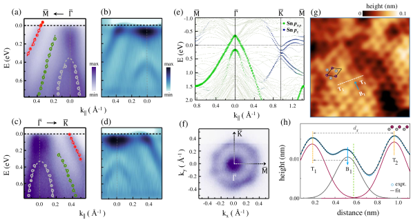
Figure 1(a) shows an inverted “V”-like valence band of MBST with its maximum close to at the point, as has been reported in literature [27, 28, 29]. It disperses from the maximum down to about 0.3 eV binding energy () at 0.2 Å-1. The substitution of Bi by Sb induces p-type doping in MBST [27] causing the band maximum to appear close to in contrast to MBT, where it is observed 0.4 eV below due to the inherent n-type doping [25].
An intriguing observation with Sn deposition is a gradual, rigid band-like shift of the MBST bulk valence band maximum towards larger [Fig. 1(b-e)]. A quantitative estimate of this shift is about 70 meV for a deposition time () of 1.2 min, which is obtained by fitting the energy distribution curves (EDCs) drawn at = 0 with Lorentzian functions; see Supplementary Fig. 2. The ARPES intensity plots towards the direction also show a similar shift of the band maximum; see Supplementary Fig. 3. The observed shift contrasts with the effect of p-type doping by Sb and indicates that Sn deposition results in n-type doping. This implies the formation of a chemical bond between Sn and the substrate due to charge transfer. Note that Fig. 1(a-e) shows that the shift is gradual with , while, on the other hand, a discontinuous shift is expected across an intrinsic bulk band gap (0.2 eV for MBST). So, the observed gradual shift suggests the presence of the in-gap topological surface states [27, 28], but these states are not observed directly in our ARPES data recorded with 21.2 eV He I radiation due to the photoemission matrix element effect [25].
For the largest deposition of = 4.8 min, the ARPES intensity plot undergoes a transformation as new bands emerge [Fig. 1(h)]. An outer hole-like band indicated by black arrows is observed to disperse from close to at about 0.36 Å-1 to 0.4 eV at 0.5 Å-1. In addition, a weak inner hole-like band – highlighted by green arrows – is also visible. At a relatively smaller Sn deposition of = 3.6 min in Fig. 1(g), the outer band is also visible (black arrows). At = 2.4 min, this band is fainter [Fig. 1(f)], but is clearly identified in the second derivative ARPES intensity plot in Supplementary Fig. 4 that reveals bands with better contrast, as shown by our earlier works [17, 47]. These new outer and inner bands are associated with stanene, as discussed in the next section.
Stanene on MBST
-: Figure 2(a) shows the outer and inner bands towards the - direction with better statistics measured at 80 K [Fig. 2(b) shows the second derivative ARPES intensity plot]. The dispersion of the outer hole band is depicted by red open circles. These circles correspond to the maximum intensity of the momentum distribution curves (MDCs) at different (Supplementary Fig. 5 shows how the maximum is identified by fitting). The red dashed line, which is a linear fit to the red circles, shows that the dispersion is a close approximation to linearity. The inner hole band (green dashed line), determined in a similar way, disperses down to 0.8 eV at 0.4 Å-1. An inverted parabolic band is also observed that disperses from a maximum of 0.4 eV at to 0.8 eV at 0.2 Å-1.
To find the origin of the above discussed bands, in Fig. 2(e) we show the calculated band dispersion of monolayer stanene on MBT by using first principles DFT, including spin-orbit coupling [the structure is shown in Supplementary Fig. 1(a)]. The green and blue circles represent the Sn and contributions to the stanene bands, respectively, obtained by projecting the Bloch wave function on these orbitals. An outer band of Sn character crosses and has nearly linear dispersion in the experimentally studied - range. The inner band, also arising from Sn orbitals, has a maximum below around the point and disperses down to about 1 eV. It is weaker compared to the outer band, in fair agreement with ARPES. The presence of both the experimentally observed inner and outer bands [Fig. 2(a,b)] in the DFT calculation [Fig. 2(e)] indicates the formation of stanene. Based on the DFT calculation and STM discussed later in the final subsection, the inverted parabolic band observed from ARPES in Fig. 2(a,c) – but not from DFT of monolayer stanene in Fig. 2(e) – has been related to bilayer stanene.
To experimentally probe whether the outer band crosses , we have deposited potassium (K), which provides electrons to the surface that would fill up this band [48, 5]. Thus, the band positions above can be determined. As shown by the red filled circles in Fig. 2(a) (the corresponding ARPES intensity plots shown in Supplementary Fig. 6), we find that the outer band crosses , which is in agreement with DFT [Fig. 2(e)].
-: The outer and inner stanene bands towards the - direction are observed in ARPES [Fig. 2(c,d)], which are highlighted by open circles and the dashed lines in Fig. 2(c). These are in fair agreement with the DFT calculated bands in this direction [Fig. 2(e)]. Furthermore, ARPES shows that the outer band crosses at a slightly larger Fermi vector compared to -. This observation is consistent with the hexagonal symmetry of the Fermi surface in Fig. 2(f) that gives of 0.4 Å-1 towards - compared to - (= 0.35 Å-1). Hexagonal Fermi surface of stanene has been observed on Bi2Te3 [32] and PdSn2 [37]. In fact, a series of - isosurface plots for varying from 0.1 to 0.4 eV in Supplementary Fig. 7 also exhibits the hexagonal symmetry.
Note that the Fermi velocity of stanene (estimated from the slope of the outer band) towards - and - are similar, i.e., 3.20.02105 m/s. This value is somewhat larger compared to stanene on Bi2Te3 (2.79105 m/s) [32] or Sb2Te3 (2.83105 m/s) [49], indicating that stanene on MBST may be useful in high-speed electronic devices.
The Sn related bands from DFT calculation appear near at the point [Fig. 2(e)], whereas from ARPES, we observe a large bandgap with a band shifted down to 0.85 eV (Supplementary Fig. 8). This disagreement with DFT has also been observed earlier for stanene on Bi2Te3 [5] and PbTe [7], where an experimental band was likewise shifted to larger opening up a large gap at . Based on the DFT calculation of hydrogen passivated stanene [1, 7], this disagreement has been related to the passivation of the reactive Sn orbital by hydrogen. This is also possibly the reason for the discrepancy observed by us.
STM: An STM topography image of stanene with atomic resolution displayed in Fig. 2(g) reveals three Sn atoms as distinct bright spots (magenta circles), which are interconnected by somewhat less bright areas (gray circles). Figure 2(h) displays an average height profile obtained along the trajectory indicated in Fig. 2(g) by a white dashed line that joins two bright spots labeled by T1 and T2, as well as a less bright region B1 (blue arrow). In the height profile, T1 and T2 produce two distinct peaks, whereas B1 results in a shoulder. In order to ascertain their positions, three Gaussian functions with nearly similar full width at half maxima have been employed to fit the profile. The quality of the fitting is good, as shown by the fitted curve, and the separation between T1 and T2 turns out to be = 0.02 nm. This is the longer diagonal of the primitive unit cell of stanene, shown by black lines in Fig. 2(g). The lattice constant of stanene (), given by /, is thus determined to be 0.460.01 nm. This value is similar to that found from the fast Fourier transform method.
A confirmation that Fig. 2(g) represents stanene is based on the observation that B1 is not at /2 [green dashed vertical line in Fig. 2(h)], but is closer to T1. This asymmetry is a litmus test for stanene formation that stems from the contribution of intensity to B1 by the Sn atoms in the lower sublattice. To establish that the asymmetry is not due to drift that is often present in STM images, we have measured the profiles over multiple unit cells along three different directions (d1, d2, and d3) and also parallel to these directions [see Supplementary Fig. 9(a)]. Supplementary Fig. 9(b) shows the average of each direction for three consecutive unit cells, in each case, B1 shows the asymmetry. The average value of T1B1 is 0.340.04 nm. This is comparable to the ideal value of /3 (= 0.27 nm) obtained when a buckled hexagon is projected on the horizontal plane. The difference in height between B1 and T1 indicates the presence of buckling; a schematic diagram of buckled stanene is shown in the inset of Fig. 2(h).
The asymmetry in position of B1 distinguishes the honeycomb structure of stanene from the triangular lattice of the MBST surface. A similar analysis for MBST shows a shoulder exactly at /2, in this case, it is attributed to the residual contribution of the Te atoms connected by the smaller diagonal of the unit cell (Supplementary Fig. 10). The lattice constant of MBST is found to be 0.430.02 nm, which is smaller compared to that of stanene (0.46 nm). However, this value is similar to that of bulk MBST from x-ray diffraction (0.4304 nm) [50], indicating that lateral surface relaxation is not significant in MBST.
Buffer layer formation and signature of stanene from XPS and LEED
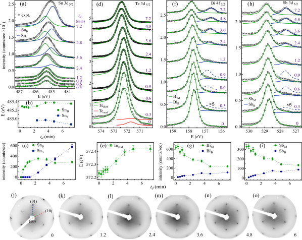
Sn 3: The XPS spectra in Fig. 3(a) show the signature of two components of Sn 3 for 2.4 min. These are SnS (blue curve, assigned to the stanene component, discussed later) and SnB (green curve, assigned to the buffer layer (BL) component, discussed here). These components are obtained by least squares fitting, see also Supplementary Fig. 11 that shows each spectrum normalized to the same height along with the components, background, and residual of the fitting, and Supplementary Table I that gives the converged fitting parameters with their errors. In contrast, for 2.4 min, the spectra are well fitted with only one component, SnB. SnB appears at 485.3 eV [Fig. 3(b)] that is significantly shifted to a larger from bulk Sn metal (484.7 eV). Rather, of SnB is close to SnTe (485.4 eV [32, 51]) indicating that the Sn atoms react with the top Te layer of the (0001) surface of MBST (Supplementary Fig. 1) forming Sn-Te bonds by transferring electrons, which is also supported by ARPES [Fig. 1(a-e)]. This is also consistent with the smaller tendency of Sn to gain electrons (i.e., the electronegativity of Sn is 1.96 in the Pauling scale [52]) compared to Te (2.1 [52]). The reaction between Sn and Te contributes to the formation of the BL. The BL related component, SnB, is visible right from the beginning at = 0.3 min and increases rapidly in intensity up to = 2.4 min as the BL grows, but stagnates thereafter [Fig. 3(c)]. As discussed later in Fig. 4(c), an STM topography image shows that the BL is almost fully formed and covers more than 90% of the surface at = 2.4 min.
Te 3: In Fig. 3(d,e), the effect of Sn-Te bonding on the Te 3 core level spectra is manifested as a shift towards larger with respect to bare MBST. The spectra can be fitted with a single component denoted as TeBM comprising of (i) TeB i.e., the Te 3 signal from the BL that reacts with Sn forming Sn-Te like bonds, and (ii) TeM i.e., the Te 3 signal from the deeper Te layers that do not react with Sn (see Supplementary Fig. 12 and Supplementary Table II for details of fitting). TeM and TeB are not resolved as separate peaks within our resolution. This is because the of TeM is 572.2 eV [determined from the bottom spectrum in Fig. 3(d) i.e., MBST], which is close to that of TeB (572.3 eV [51], which is the of Te 3 in SnTe).
Note that a surface core level peak, Tesurf, is observed for MBST (= 0) that is shifted by 0.5 eV towards lower from the main peak [red curves in Fig. 3(d)]. In Supplementary Fig. 13, it is confirmed by a difference spectrum between = 0 min and 0.3 min, where it is suppressed in the latter due to a change in the surface potential caused by Sn deposition. Such surface core level peak – reported in other Te terminated surfaces [53, 54]– are generally related to a reduction in the coordination number of the surface Te atoms.
Bi 4 and Sb 3: The analysis of the Bi 4 and Sb 3 core level spectra in Fig. 3(f,h), respectively, provides additional insight into the BL, where both Bi and Sb (referred to together as “Bi/Sb”) show a component (Bi/Sb)B (blue curve, BL component) in addition to the main peak, (Bi/Sb)M (green curve, bulk component from deeper layers). See also Supplementary Fig. 14-15 and Supplementary Tables III-IV for the details of the fitting. BiB and SbB appear at 156.85 eV and 527.65 eV, which are shifted by 0.85-1.2 and 1.15 eV, respectively, towards lower compared to their respective main peaks. This significant shift in (Bi/Sb)B suggests chemical bonding between Sn and Bi/Sb from the beginning, i.e., = 0.3 min. ’s of (Bi/Sb)B are smaller compared even to their corresponding elemental bulk values (156.9 and 528.2 for Bi and Sb, respectively [51]). This points to a bonding with Sn that would transfer electrons to Bi/Sb due to the larger electronegativity of Bi/Sb (2.02/2.05 [52]) compared to Sn (1.96). The (Bi/Sb)B component has finite intensity from the outset (= 0.3 min) [see the five times magnified blue dashed curves in Fig. 3(f,h) and the intensity variation in Fig. 3(g,i)] indicating the formation of Sn-Bi/Sb bonds, although Bi/Sb is below the Te layer (Supplementary Fig. 1). The BL related component is also observed in the Bi 5 core level spectra taken with He II radiation (40.8 eV) at a similar separation from the main peak (Supplementary Fig. 16). The Mn 2 spectrum of MBST [25] is hardly influenced by Sn deposition (Supplementary Fig. 17). This observation indicates that the Mn layer, which is the fourth layer of the septuple, has minimal interaction with Sn and is unlikely to play a role in the formation of the BL.
Stanene related SnS component: The SnS component of Sn 3 is related to stanene because it is observed only for 2.4 min, when stanene related bands are visible in ARPES (Fig. 1,2). It is zero for 1.2 min [Fig. 3(c)], where neither ARPES nor STM [Fig. 4(a)] detect the stanene signature. SnS appears at = 484.95 eV and becomes more intense than SnB at = 4.8 min, where the stanene bands are unambiguously observed in ARPES [Fig. 2(a-d)]. Supplementary Fig. 16 shows the SnS component at = 25.1 eV in the Sn 4 spectrum acquired with He II radiation, shifted with respect to the SnB component at = 25.5 eV. This shift is similar to that observed in Sn 3. The SnS component in Sn 4 is observed as a distinct peak (unlike in Sn 3 from XPS) due to the improved energy resolution with He II. In addition, the low kinetic energy of the photoelectrons enhances the surface sensitivity in this case. Since stanene grows on the BL, surface sensitivity causes the Sn 4 related SnS component to be more intense than the SnB component; compare Fig. 3(a) and Supplementary Fig. 16 for 4.8 min.
Composition of BL: The composition of the BL has been estimated from XPS to be 54% Sn, 23% Te, 13% Bi, and 10% Sb after averaging for 2.4 min i.e., after it is fully formed (see the Methods section). Therefore, the approximate ratio of Sn:Te:Bi/Sb atoms in the BL is 2:1:1. This shows that the BL comprises of Sn atoms that bond with a nearly equal number of Te and Bi/Sb atoms implying that two Sn atoms per unit cell are required to form the BL.
LEED for different : A set of LEED patterns in Fig. 3(j-o) demonstrates epitaxial growth for all depositions, in spite of the BL formation. (11) spots are observed throughout with no evidence of splitting or broadening. The symmetry of the BL remains similar to the substrate, as shown by Fig. 3(j-l). An additional important observation from Fig. 3(j-l) is that the background to the spot intensity ratio increases quite substantially for the BL compared to MBST. This is shown quantitatively in Supplementary Fig. 18 from the intensity profiles along (00) to (01) spot and (00) to (10) i.e., the blue and red dashed lines, respectively in Fig. 3(j); the (00) spot is at the center of the pattern but is covered by the shadow of the electron source, and all the profiles are aligned to it. Supplementary Fig. 18(c) shows the ratio of the background () and the spot () intensities, which is maximum at = 2.4 where the BL is fully formed. Such an increase in the background intensity in the LEED pattern has been related to the existence of random anti-site defects in previous literature [55, 56]. (Bi/Sb)Te anti-site defects, where Bi/Sb atoms of the second layer are exchanged with the Te atoms of the top layer, are already present in MBST. In agreement with previous literature [57, 58], these defects have been observed as bright protrusions in the STM image [Supplementary Fig. 10(c)]. With Sn deposition, the anti-site defects are enhanced, possibly because of the propensity for chemical bonding aided by the kinetic energy of the impinging Sn atoms (equal to 1073 K) and the similarity of their atomic diameters (0.278 nm, 0.276 nm, 0.296 nm, and 0.278 nm for Sn, Te , Bi, and Sb, respectively [59]).
In Supplementary Fig. 18(a,b), position of the (01) peak for the BL (= 1.2-2.4 min) is shifted towards lower compared to that of MBST (= 0 min) showing that its separation with the (00) spot decreases by about 4%. A similar decrease is also observed for the (10) spot. This indicates that the lattice constant of the BL increases by 4% compared to MBST. On the other hand, the separation of the peak positions for the BL hardly shows any difference compared to stanene (3.6 min). This shows that the lattice constant of stanene is similar to the BL. Thus, in agreement with STM, LEED shows that the lattice constant of stanene is larger compared to MBST. This difference in their lattice constant is bridged by the BL.
Bilayer stanene formation from STM and DFT
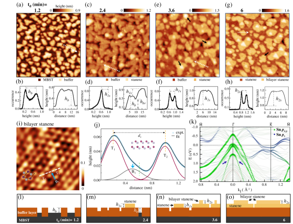
At the initial stage (= 1.2 min), where both ARPES and XPS indicate the formation of BL without any signature of stanene, Fig. 4(a) shows that about 60% of the substrate is covered by the BL that are manifested as islands of height = 0.50.05 nm measured from the uncovered Te top layer of MBST (dark brown region) [Fig. 4(b)]. Thus, is due to Sn deposition and is larger than the typical thickness of a Sn monolayer (0.18-0.38 nm) grown on different substrates [2, 31, 5, 33, 34, 6, 60, 61]. Rather, is close to twice the covalent diameter of Sn (0.278 nm [59]), indicating that two Sn atoms per unit cell would be required for BL formation, as has been shown earlier by its composition determined from XPS. Despite the admixture of Sn with Te and Bi/Sb in the BL islands caused by chemical bonding and anti-site defect formation, the validity of the aforementioned argument holds due to the similarity in their sizes [59]. The total thickness of the BL, including the thickness of the Te and Bi/Sb layers, is estimated to be 0.9 nm, where the thickness of the top two layers of MBST is taken to be 0.4 nm from x-ray crystallography [50].
In Fig. 4(c) for 2.4 min deposition, the almost fully formed BL covers more than 90% of the substrate. Its height is similar to that of previous deposition, but there are some less darker regions where the height is however smaller than 0.5 nm. This is also indicated by the asymmetry in the height histogram around 0.3 nm [Fig. 4(d)]. An example of the reduced height of the BL is shown by in the height profile. Thus, the BL has a somewhat non-uniform thickness. This is reflected by its enhanced mean square roughness () of 0.12 (0.14)0.025 nm at = 1.2 (2.4) min estimated by masking the uncovered substrate. It is important to note that further Sn deposition smoothens the BL, e.g., becomes 0.080.01 nm for = 3.6 min that is close to that of the substrate (= 0.070.01 nm), thus enabling growth of stanene.
Curiously in Fig. 4(c), some white islands on the BL that have a step height of and cover 10% of the area are visible, where a stanene signature is also observed in XPS [Fig. 3(a)]. In Fig. 4(e) at = 3.6 min, these islands increase in size with similar that covers about 65% of the BL. These islands represent stanene, as shown earlier by the atomic resolution image and its analysis in Fig. 2(g,h). From the height histogram and profile in Fig. 4(f), turns out to be 0.350.02 nm. This is close to the step height of 0.35 nm reported for buckled stanene on other substrates such as Bi2Te3 [5].
Figure 4(g) shows the unambiguous signature of bilayer stanene i.e., a second layer stanene island on the monolayer stanene; one such island is highlighted by a black arrow. Figure 4(h) shows the height of these islands to be 0.350.03 nm (= ). Its atomic resolution image is shown in Fig. 4(i), where the unit cell (black line) joins four Sn atoms visible as bright spots (magenta circles) of the upper sublattice (the lower sublattice atoms are shown by gray circles). In Fig. 4(j), the average height profile along the white dashed line in Fig. 4(i) and its analysis [see also Supplementary Fig. 9(c)] reveals that it is buckled with a lattice constant (= /) similar to monolayer stanene. This analysis establishes bilayer stanene formation over 60% of the total area of Fig. 4(g).
DFT calculation has been performed for bilayer stanene with the structure shown in Supplementary Fig. 1(b). The calculated bands show – besides the outer and inner bands – an inverted parabolic band (highlighted by blue arrows) towards both and directions, with the maximum at at 0.5 eV [Fig. 4(k)]. Supplementary Fig. 19 shows that the inverted parabolic band has a nearly equal contribution from the Sn and orbitals. The outer and inner stanene bands also have similar Sn and contributions for both monolayer and bilayer stanene. The Sn related bands appear more than 1 eV above with a minimum at in both cases.
It is important to point out that the inverted parabolic band observed in the ARPES intensity plots [Fig. 2(a-d)] closely resembles the unexplained band that was not present in the DFT band structure of monolayer stanene [Fig. 2(e)]. Thus, this band’s origin is associated with bilayer stanene. Evidence of bilayer stanene formation comes from the islands highlighted by black arrows in Fig. 4(e), whose area would obviously increase at = 4.8 min where ARPES has been performed. Thus, the growth of bilayer stanene islands commences on the monolayer stanene islands prior to the latter’s complete coverage of the BL, which is a characteristic of Stranski-Krastanov growth.
Finally, it is worth noting that despite considering MBT as the substrate and not the BL, our DFT calculations identify all the stanene-related bands observed in ARPES, albeit with somewhat shifted energies and momenta. This fairly good agreement with DFT indicates that the coupling of the BL with stanene is weak. Thus, the BL provides a non-reactive platform to facilitate the growth of stanene on MBST.
In conclusion, using a combination of complementary analytical techniques, we report the discovery of bilayer stanene on a magnetic topological insulator (MBST), whose growth is aided by the formation of an underlying buffer layer. A series of schematic diagrams is used to represent the complete narrative as a function of Sn deposition in Fig. 4(l-o). For the initial depositions, ARPES shows a gradual shift of the MBST band, indicating electron transfer due to buffer layer formation. The characteristic stanene bands, such as the hole-like outer and inner bands and an inverted parabolic band appear for further Sn deposition. These bands are observed in our DFT calculation for buckled stanene on MBT; in particular, the inverted parabolic band is assigned to bilayer stanene. Evidence of monolayer and bilayer stanene formation is also obtained from the atomic resolution STM images. The buffer layer plays an important role because it quenches the tendency of chemical bonding of the Te and Bi/Sb atoms with Sn, thus providing a non-reactive platform to facilitate the growth of stanene. Buckled stanene grows as islands with a height of 0.35 nm on the buffer layer of 0.9 nm thickness that has an approximate composition ratio of Sn:Te:Bi/Sb of 2:1:1.
Formation of bilayer stanene opens up the possibility of superconductivity [7, 6] and its ensuing proximity effect on MBST that is antiferromagnetic below 24 K [Supplementary Fig. 20(a)]. The proximity effect could be tuned by varying the thickness of the buffer layer through modification of the growth conditions. The buffer layer could also possibly become superconducting, as there are reports in literature about superconductivity in Sn0.57Sb0.43 with = 1.45 K [62] and Sn1-δTe with 0.3 K [63], both having rhombohedral structure as is the case here. Our work establishes the formation of bilayer stanene on a magnetic topological insulator, which may lead to interesting interplay between band topology, superconductivity, and magnetism.
Methods
ARPES and XPS: A helium discharge lamp with a monochromator was utilized as the radiation source with photon energy 21.2 eV for the ARPES measurements. The ejected photoelectrons were detected with an acceptance angle of using the R4000 hemispherical electron energy analyzer from Scienta Omicron GmbH with the energy resolution set at better than 15 meV, while the angular resolution was 1∘. The XPS measurements were performed using a monochromatized AlKα radiation source with a photon energy of 1486.6 eV using the transmission lens mode. The energy resolution was 0.33 eV. The LEED equipment comprised of a four-grid rear-view optics system.
The analysis of the photoemission data was performed using Igor Pro, ver 9 from Wavemetrics Inc. The core level spectra were fitted with the least square error minimization method as in our earlier works [64, 38] with the instrumental resolution represented by a Gaussian function of fixed width. The energy position, intensity, life-time broadening, and the Tougaard background [65] parameter were varied during the fitting. The intensities are plotted from the areas under the component curves and the composition of the BL has been determined from the areas of the SnB, TeB, BiB , and SbB components after dividing by their respective photoemission cross sections [66] and the analyzer transmission function. Since Te 3 does not show a distinguishable BL component, TeB has been extracted from the total Te signal, TeBM, by calculating the contribution of the top or first Te layer that is involved in the BL formation using the equation e. Here, = intensity of the Te layer, = intensity of the top layer, = depth of the Te layer from the top surface, and is the inelastic mean free path [67] calculated by weighted averaging for the atoms in the region through which the electrons emitted from the Te layer passes to reach the surface. For example, = 20.95 (19.8) nm for = 2 (3) and is nearly unchanged at 20.2 nm for 8. We consider the intensity contribution to Te 3 signal from the first to the Te layer in the 6th septuple, contribution of the latter being 2% compared to the first Te layer. The total intensity measured is thus given by, , which gives the first Te layer contribution or TeB to be Here, ’s are taken from the reported crystal structure of MBST [50]. Thus, TeB turns out to be about 16% of TeBM. The compositions determined this way is not affected by stanene formation indicating that it attenuates all the BL components in similar manner. So, the composition of the BL mentioned in the main text has been averaged over the compositions determined for four values that are 2.4 min and the error turns out to be about 7.5%.
STM: The STM measurements were performed using a variable temperature STM (VT-STM) from Scienta Omicron GmbH at a base pressure of 410-11 mbar. Electrochemically etched polycrystalline W tips as well as mechanically grinded Pt-Ir tips were used. These tips were cleaned in-situ using Ar+ ion sputtering and applying voltage pulses. The tip was biased and the sample was kept at the ground potential. The average height of each layer is calculated by averaging over more than 50 height profiles and also by height histogram, as in our earlier work [61]. All the measurements were performed at RT unless otherwise mentioned. The STM images was analyzed using the SPIP and Gwyddion software. Atomic resolution STM images are enhanced using Fourier filtering. To calculate the mean square roughness () for the BL, we have used a masking procedure to select only the islands related to the BL.
Density functional theory: The density functional theory based (DFT) first-principles calculations were performed using the projector-augmented-wave (PAW) [68] potential and the exchange correlation functional Perdew–Burke–Ernzerhof (PBE) generalized gradient approximation (GGA) [69], as implemented in the Vienna ab initio simulation package (VASP) [70]. Buckled monolayer stanene was considered in which the lower (upper) Sn sublattice is located at the hollow (face-centered cubic) site of the substrate [Supplementary Fig. 1(a)]. The bilayer stanene was considered following the -Sn structure in the (111) direction [Supplementary Fig. 1(b)]. The MBT(0001) surface was modeled by a periodic slab, including three septuple layers using the experimental lattice constants of 0.436 nm. For the slab calculations, a vacuum of 1.5 nm were applied along the direction to overcome the interactions between the periodic images. The slab calculations were performed with a plane wave basis with an energy cutoff of 400 eV, a 13131 Monkhorst-Pack grid [71] was used for the -space sampling. A force convergence criterion of 0.01 eV Å-1 was selected for structural optimization. The spin–orbit coupling interaction was included in the electronic structure calculation. The band structure calculations were performed along the high-symmetry paths (0.5, 0.0, 0.0) – (0.0, 0.0, 0.0) – (1/3, 1/3, 0.0). The VESTA program [72] has been employed for the representation and visualization of the crystal structures.
Sample preparation and characterization: Stanene was grown by deposition of Sn () using a water-cooled Knudsen cell [73] equipped with a mechanical shutter at an operating temperature of 1073 K and pressure of mbar. The substrate temperature was about 303-313 K and its distance from the Knudsen cell was 70 mm and the angle of deposition was 45∘.
In-situ peeling with a scotch tape exposed an atomically clean (0001) surface of the substrate MBST crystal. The peeling was performed at room temperature at a pressure of mbar. The MBST single crystal was grown by the flux method following a similar temperature profile described in previous reports [74, 28]. In order to grow % Sb doped MBST crystal, a mixture of Mn powder (Alfa Aesar, 99.95%), Bi shots (Furuchi Chemical Corporation, 99.999%), Te chunks (Furuchi Chemical Corporation, ), and Sb shots (Alfa Aesar, 99.999%) in a molar ratio Mn: Sb: Bi: Te = 1: 10: 10: 16 were placed in an alumina crucible of a Canfield crucible set. A thin quartz wool pad was also placed between the bottom crucible containing the above mentioned chemicals and the frit-disk to minimize cracks on crystals during centrifuge. Then, the entire crucible set was sealed in an evacuated silica ampule at mbar pressure. The sealed ampule was heated to 1173 K for two days and kept at that temperature for 12 hours followed by a slow cooling 10 K/hr down to 878 K. At the final stage of the temperature profile, the ampule was cooled from 878 K to 863 K in 336 hrs and kept at that temperature for 72 hrs followed by centrifuge at 3000 rpm to remove the excess flux from crystals. Plate-like shiny crystals with dimensions of a few millimeters, shown in the inset of Supplementary Fig. 20(a), are obtained from the bottom crucible. From the XPS core level spectra presented in Fig. 3(f,h), we have confirmed that the amount of Sb doping is in agreement with the intended composition. In agreement with literature [27, 74], magnetization () versus temperature at a magnetic field () of 0.1 Tesla shows the Neel temperature to be 24 K, whereas measurement at 2 K shows the spin flop transition from antiferromagnetic to canted antiferromagnetic at 2.3 Tesla (Supplementary Fig. 20).
Data availability
The data that support the findings of this study are available from the corresponding author upon reasonable request.
References
- Xu et al. [2013] Xu, Y. et al., Large-gap quantum spin Hall insulators in tin films, Phys. Rev. Lett. 111, 136804 (2013).
- Deng et al. [2018] Deng, J. et al., Epitaxial growth of ultraflat stanene with topological band inversion, Nat. Mater. 17, 1081 (2018).
- Novoselov et al. [2004] Novoselov, K. S. et al., Electric field effect in atomically thin carbon films, Science 306, 666 (2004).
- Geim and Novoselov [2007] Geim, A. K. and Novoselov, K. S., The rise of graphene, Nat. Mater. 6, 183 (2007).
- Zhu et al. [2015] Zhu, F.-f. et al., Epitaxial growth of two-dimensional stanene, Nat. Mater. 14, 1020 (2015).
- Zhao et al. [2022] Zhao, C. et al., Coexistence of robust edge states and superconductivity in few-layer stanene, Phys. Rev. Lett. 128, 206802 (2022).
- Liao et al. [2018] Liao, M. et al., Superconductivity in few-layer stanene, Nat. Phys. 14, 344 (2018).
- Fu and Kane [2008] Fu, L. and Kane, C. L., Superconducting proximity effect and majorana fermions at the surface of a topological insulator, Phys. Rev. Lett. 100, 096407 (2008).
- Shoman et al. [2015] Shoman, T. et al., Topological proximity effect in a topological insulator hybrid, Nat. Commun. 6, 6547 (2015).
- Trang et al. [2020] Trang, C. X. et al., Conversion of a conventional superconductor into a topological superconductor by topological proximity effect, Nat. Commun. 11, 159 (2020).
- Charpentier et al. [2017] Charpentier, S. et al., Induced unconventional superconductivity on the surface states of Bi2Te3 topological insulator, Nat. Commun. 8, 2019 (2017).
- Oliveira et al. [2015] Oliveira, M. H. et al., Synthesis of quasi-free-standing bilayer graphene nanoribbons on SiC surfaces, Nat. Commun. 6, 7632 (2015).
- Du et al. [2016] Du, Y. et al., Quasi-freestanding epitaxial silicene on Ag(111) by oxygen intercalation, Sci. Adv. 2, e1600067 (2016).
- Chen et al. [2009] Chen, Y. L. et al., Experimental realization of a three-dimensional topological insulator, Bi2Te3, Science 325, 178 (2009).
- Zhang et al. [2009] Zhang, H. et al., Topological insulators in Bi2Se3, Bi2Te3 and Sb2Te3 with a single Dirac cone on the surface, Nat. Phys. 5, 438 (2009).
- Poudel et al. [2008] Poudel, B. et al., High-thermoelectric performance of nanostructured bismuth antimony telluride bulk alloys, Science 320, 634 (2008).
- Sarkar et al. [2023] Sarkar, S. et al., Charge density wave induced nodal lines in LaTe3, Nat. Commun. 14, 3628 (2023).
- Ali et al. [2014] Ali, M. N. et al., Large, non-saturating magnetoresistance in WTe2, Nature 514, 205 (2014).
- Aharon-Steinberg et al. [2022] Aharon-Steinberg, A. et al., Direct observation of vortices in an electron fluid, Nature 607, 74 (2022).
- Kang et al. [2015] Kang, D. et al., Superconductivity emerging from a suppressed large magnetoresistant state in tungsten ditelluride, Nat. Commun. 6, 7804 (2015).
- Wang et al. [2019] Wang, Z., Wieder, B. J., Li, J., Yan, B. and Bernevig, B. A., Higher-order topology, monopole nodal lines, and the origin of large Fermi arcs in transition metal dichalcogenides, Phys. Rev. Lett. 123, 186401 (2019).
- Otrokov et al. [2019] Otrokov, M. M. et al., Prediction and observation of an antiferromagnetic topological insulator, Nature 576, 416 (2019).
- Li et al. [2019a] Li, J. et al., Intrinsic magnetic topological insulators in van der Waals layered MnBi2Te4-family materials, Sci. Adv. 5, eaaw5685 (2019a).
- Gao et al. [2023] Gao, A. et al., Quantum metric nonlinear Hall effect in a topological antiferromagnetic heterostructure, Science 381, 181 (2023).
- Chen et al. [2019a] Chen, Y. J. et al., Topological electronic structure and its temperature evolution in antiferromagnetic topological insulator MnBi2Te4, Phys. Rev. X 9, 041040 (2019a).
- Li et al. [2019b] Li, H. et al., Dirac surface states in intrinsic magnetic topological insulators EuSn2As2 and MnBi2nTe3n+1, Phys. Rev. X 9, 041039 (2019b).
- Chen et al. [2019b] Chen, B. et al., Intrinsic magnetic topological insulator phases in the Sb doped MnBi2Te4 bulks and thin flakes, Nat. Commun. 10, 4469 (2019b).
- Ma et al. [2021] Ma, X.-M. et al., Realization of a tunable surface Dirac gap in Sb-doped MnBi2Te4, Phys. Rev. B 103, L121112 (2021).
- Glazkova et al. [2022] Glazkova, D. A. et al., Electronic structure of magnetic topological insulators Mn(Bi1-xSbx)2Te4 with various concentration of Sb atoms, JETP Letters 115, 286 (2022).
- Xu et al. [2017] Xu, C.-Z. et al., Elemental topological Dirac semimetal: -Sn on InSb(111), Phys. Rev. Lett. 118, 146402 (2017).
- Yuhara et al. [2018] Yuhara, J. et al., Large area planar stanene epitaxially grown on Ag(111), 2D Mater. 5, 025002 (2018).
- Li et al. [2020a] Li, J. et al., Anisotropic electronic structure and interfacial chemical reaction of stanene/Bi2Te3, J. Phys. Chem. C 124, 4917 (2020a).
- Zheng et al. [2019] Zheng, X., Zhang, J.-F., Tong, B. and Du, R.-R., Epitaxial growth and electronic properties of few-layer stanene on InSb (111), 2D Mater. 7, 011001 (2019).
- Gou et al. [2017] Gou, J. et al., Strain-induced band engineering in monolayer stanene on Sb(111), Phys. Rev. Mater. 1, 054004 (2017).
- Sadhukhan et al. [2020] Sadhukhan, P. et al., Electronic structure and morphology of thin surface alloy layers formed by deposition of Sn on Au(111), Appl. Surf. Sci. 506, 144606 (2020).
- Shah et al. [2021] Shah, J., Wang, W., Sohail, H. M. and Uhrberg, R. I. G., Atomic and electronic structures of the surface alloy on Au(111), Phys. Rev. B 104, 125408 (2021).
- Yuhara et al. [2021] Yuhara, J. et al., In-plane strain-free stanene on a Pd2Sn(111) surface alloy, Phys. Rev. Mater. 5, 053403 (2021).
- Sadhukhan et al. [2019] Sadhukhan, P. et al., Electronic structure of Au-Sn compounds grown on Au(111), Phys. Rev. B 100, 235404 (2019).
- Pesin and MacDonald [2012] Pesin, D. and MacDonald, A. H., Spintronics and pseudospintronics in graphene and topological insulators, Nat. Mater. 11, 409 (2012).
- Molle [2016] Molle, A., Xenes: A new emerging two-dimensional materials platform for nanoelectronics, ECS Trans. 75, 163 (2016).
- Wang et al. [2023] Wang, M., Hu, Y., Pu, J., Zi, Y. and Huang, W., Emerging Xene-based single-atom catalysts: Theory, synthesis and catalytic applications, Adv. Mater. , 2303492 (2023).
- Tao et al. [2019] Tao, W. et al., Emerging two-dimensional monoelemental materials (Xenes) for biomedical applications, Chem. Soc. Rev. 48, 2891 (2019).
- Deng et al. [2020] Deng, Y. et al., Quantum anomalous Hall effect in intrinsic magnetic topological insulator MnBi2Te4, Science 367, 895 (2020).
- Haldane [1988] Haldane, F. D. M., Model for a quantum Hall effect without Landau levels: Condensed-matter realization of the “parity anomaly”, Phys. Rev. Lett. 61, 2015 (1988).
- Yu et al. [2010] Yu, R. et al., Quantized anomalous Hall effect in magnetic topological insulators, Science 329, 61 (2010).
- Zhang et al. [2013] Zhang, J. et al., Topology-driven magnetic quantum phase transition in topological insulators, Science 339, 1582 (2013).
- Singha et al. [2023] Singha, R. et al., Signatures of topological surface state and unconventional magnetotransport properties in elemental ruthenium, Adv. Quantum Technol. 6, 2200116 (2023).
- Neupane et al. [2012] Neupane, M. et al., Topological surface states and Dirac point tuning in ternary topological insulators, Phys. Rev. B 85, 235406 (2012).
- Li et al. [2020b] Li, J. et al., In-plane crystal field constrained electronic structure of stanene, Appl. Phys. Lett. 116, 101601 (2020b).
- Yan et al. [2019] Yan, J.-Q. et al., Evolution of structural, magnetic, and transport properties in MnBi2-xSbxTe4, Phys. Rev. B 100, 104409 (2019).
- Shalvoy et al. [1977] Shalvoy, R. B., Fisher, G. B. and Stiles, P. J., Bond ionicity and structural stability of some average-valence-five materials studied by x-ray photoemission, Phys. Rev. B 15, 1680 (1977).
- Mann et al. [2000] Mann, J. B., Meek, T. L. and Allen, L. C., Configuration energies of the main group elements, J. Am. Chem. Soc. 122, 2780 (2000).
- Leiro et al. [2006] Leiro, J. A., Heinonen, M. H., Mattila, S. and Szczerbakow, A., Surface core-level shifts in CdTe1-xSx(110) and CdTe1-xSex(110), Phys. Rev. B 73, 205323 (2006).
- Prince et al. [1988] Prince, K., Paolucci, G., Cháb, V., Surman, M. and Bradshaw, A., Surface core level shifts of a II–VI compound: CdTe, Surf. Sci. 206, L871 (1988).
- Janzen et al. [2001] Janzen, A., Dumkow, I. and von Hoegen, M. H., Thermal activation of dislocation array formation, Appl. Phys. Lett. 79, 2387 (2001).
- Zielasek et al. [2000] Zielasek, V., Hildebrandt, T. and Henzler, M., Surface color centers on epitaxial NaCl films, Phys. Rev. B 62, 2912 (2000).
- Garnica et al. [2022] Garnica, M. et al., Native point defects and their implications for the Dirac point gap at MnBi2Te4 (0001), npj Quantum Mater. 7, 7 (2022).
- [58] Lüpke, F. et al., Anti-site defect-induced disorder in compensated topological magnet MnBi2-xSbxTe4, arXiv:2208.13374 .
- Cordero et al. [2008] Cordero, B. et al., Covalent radii revisited, Dalton Trans. , 2832 (2008).
- Singh et al. [2020] Singh, V. K. et al., Quasiperiodic ordering in thick Sn layer on -Al-Pd-Mn: A possible quasicrystalline clathrate, Phys. Rev. Res. 2, 013023 (2020).
- Singh et al. [2023] Singh, V. K. et al., Decagonal Sn clathrate on -Al-Ni-Co, Phys. Rev. B 107, 045410 (2023).
- Liu et al. [2019] Liu, B. et al., Superconducting phase diagram and nontrivial band topology of structurally modulated Sn1-xSbx, Phys. Rev. Mater. 3, 084603 (2019).
- Erickson et al. [2009] Erickson, A. S., Chu, J.-H., Toney, M. F., Geballe, T. H. and Fisher, I. R., Enhanced superconducting pairing interaction in indium-doped tin telluride, Phys. Rev. B 79, 024520 (2009).
- Biswas et al. [2004] Biswas, C., Shukla, A. K., Banik, S., Barman, S. R. and Chakrabarti, A., Argon nanobubbles in Al(111): A photoemission study, Phys. Rev. Lett. 92, 115506 (2004).
- Tougaard [1989] Tougaard, S., Practical algorithm for background subtraction, Surf. Sci. 216, 343 (1989).
- Trzhaskovskaya and Yarzhemsky [2018] Trzhaskovskaya, M. and Yarzhemsky, V., Dirac–Fock photoionization parameters for HAXPES applications, At. Data Nucl. Data Tables 119, 99 (2018).
- Tanuma et al. [2011] Tanuma, S., Powell, C. J. and Penn, D. R., Calculations of electron inelastic mean free paths. IX. data for 41 elemental solids over the 50 eV to 30 keV range, Surf. Interface Anal. 43, 689 (2011).
- Kresse and Joubert [1999] Kresse, G. and Joubert, D., From ultrasoft pseudopotentials to the projector augmented-wave method, Phys. Rev. B 59, 1758 (1999).
- Perdew et al. [1996] Perdew, J. P., Burke, K. and Ernzerhof, M., Generalized gradient approximation made simple, Phys. Rev. Lett. 77, 3865 (1996).
- Kresse and Furthmüller [1996] Kresse, G. and Furthmüller, J., Efficient iterative schemes for ab initio total-energy calculations using a plane-wave basis set, Phys. Rev. B 54, 11169 (1996).
- Monkhorst and Pack [1976] Monkhorst, H. J. and Pack, J. D., Special points for Brillouin-zone integrations, Phys. Rev. B 13, 5188 (1976).
- Momma and Izumi [2011] Momma, K. and Izumi, F., VESTA 3 for three-dimensional visualization of crystal, volumetric and morphology data, J. Appl. Crystallogr. 44, 1272 (2011).
- Shukla et al. [2004] Shukla, A. K. et al., Versatile UHV compatible Knudsen type effusion cell, Rev. Sci. Instrum. 75, 4467 (2004).
- Lee et al. [2021] Lee, S. H. et al., Evidence for a magnetic-field-induced ideal type-II Weyl state in antiferromagnetic topological insulator Mn(Bi1-xSbx)2Te4, Phys. Rev. X 11, 031032 (2021).
Acknowledgments
The Computer division of Raja Ramanna Centre for Advanced Technology is thanked for installing the DFT codes and providing support. R.B. would like to acknowledge the partial support from the Start-up Research Grant (SRG), SERB, Govt. of India, file no. SRG/2022/000552-G. A.P. acknowledges the Israel Council for Higher Education for a postdoctoral fellowship through the Study in Israel program. M.H. thanks the Leona M. and Harry B. Helmsley Charitable Trust grants 2018PG-ISL006 and 2112-04911 for support.
Author contributions
S.B. conducted the ARPES, XPS and LEED measurements assisted by S.S. and M.B. P.B. performed the STM and LEED measurements with significant inputs from R.B. J.B. did the DFT calculations under the supervision of A.C. The single crystals of MBST were prepared and magnetic studies were performed by A.P. and M.H. S.B. analyzed the ARPES, XPS and LEED data with help from S.S. and prepared the related figures. P.B. analyzed the STM data with inputs from R.B. and prepared the related figures. S.R.B. planned and directed the project and wrote the paper with contributions from all coauthors, in particular R.B., A.C., S.B., and P.B.
Competing interests
The authors declare no competing interests.