[1]\fnmPeter Uhd \surJepsen
1]\orgdivDTU Electro, \orgnameDepartment of Electrical and Photonics Engineering, Technical University of Denmark, \orgaddress\streetØrsteds Plads 343, \cityKongens Lyngby, \postcodeDK-2800, \countryDenmark 2]\orgdivDTU Physics, \orgnameDepartment of Physics, Technical University of Denmark, \orgaddress\streetFysikvej 311, \cityKongens Lyngby, \postcodeDK-2800, \countryDenmark
Terahertz s-SNOM reveals nanoscale conductivity of graphene
Abstract
The nanoscale contrast in scattering-type scanning near-field optical microscopy (s-SNOM) is determined by the optical properties of the sample immediately under the apex of the tip of the atomic force microscope (AFM). There are several models that describe the optical scattering of an incident field by the tip near a surface, and these models have been successful in relating the measured scattering signal to the dielectric function of the sample under the tip. Here, we address a situation that is normally not considered in the existing interaction models, namely the near-field signal arising from thin, highly conductive films in the terahertz (THz) frequency range. According to established theoretical models, highly conductive thin films should show insignificant contrast in the THz range for small variations in conductivity, therefore hindering the use of s-SNOM for nanoscale characterisation. We experimentally demonstrate unexpected but clear and quantifiable layer contrast in the THz s-SNOM signal from few-layer exfoliated graphene as well as subtle nanoscale contrast variations within graphene layers. We use finite-element simulations to confirm that the observed contrast is described by the classical electromagnetics of the scattering mechanism, suggesting that the dipole models must be reformulated to correctly describe the interaction with conductive samples.
keywords:
s-SNOM, electrical conductivity, graphene, thin films, terahertz1 Introduction
Characterization of the electrical properties of thin-film materials is crucial for developing and producing electronic components, including high-quality integrated circuits, touch-sensitive screens, and solar panels. Optical methods offer the benefit of contactless techniques for non-invasive measurements. Far-field imaging at terahertz frequencies (0.1-30 THz) has proven to be a versatile contactless approach for the investigation of the optical conductivity of materials, and especially so for the full assessment of the electric properties of large-area graphene grown by chemical vapour deposition, providing spatially resolved maps of DC conductivity, carrier concentration, Fermi energy, and electron scattering time [1, 2, 3, 4]. However, the diffraction limit prevents the investigation of smaller areas of graphene obtained by exfoliation.
Scattering-type scanning near-field optical microscopy (s-SNOM) is based on detecting variations of the scattering amplitude and phase of a light beam focused onto a sharp tip (a scanning AFM probe in modern implementations) that is brought into proximity with a sample. The technique has evolved dramatically since the initial demonstrations [5, 6]. The capability of deep sub-wavelength resolution virtually independent of wavelength [7], together with the invention of harmonic demodulation techniques for suppression of the dominant far-field contribution to the scattering signal [8, 9] have led to the commercialization and widespread use of s-SNOM in the mid-IR and near-IR regions. The technique is also a versatile tool for investigating the THz dynamics of materials on the nanoscale, including graphene and other 2D materials. The THz s-SNOM (THz-SNOM) has therefore become increasingly popular in recent years, implemented with both all-electronic sub-THz sources [10, 11, 12, 13], more widely used THz laser sources (for example, Refs. 14, 15), THz radiation from a free-electron laser [16], and pulsed broadband THz sources known from THz time-domain spectroscopy [17] (THz-TDS) [18, 19, 20, 21, 22, 23, 24]. Despite this utility, in previous reports, it has been shown that THz-SNOM provides no useful contrast when investigating certain highly conductive materials: for example, rendering few-layer graphene as indistinguishable from monolayers [19, 25].
Here, we demonstrate that THz-SNOM is, despite these earlier reported results, in fact, a versatile tool for spatially resolving the conductivity of graphene at the nanoscale. We show a readily identifiable contrast that enables a clear distinction of the layer structure of exfoliated graphene flakes and local variation of the conductivity within monolayer graphene flakes. To date, there have been no proven methods for the assessment of conductivity on the nanoscale. Our demonstration of THz-SNOM for detecting subtle sub-micron variations in the conductivity of graphene, therefore, represents an important step-forward that is relevant across several disciplines. The nondestructive and contactless nature of the measurement allows the characterization of conductive 2D materials encapsulated in hexagonal boron nitride (hBN) and exotic materials such as twisted bilayers, where Moiré effects can also influence the local electronic properties. Other nanoscale probes cannot directly determine the conductivity. For instance, scanning tunneling microscopy (STM) measures the density of states of electrons in the surface of materials—not the conductivity.
2 Results and Discussion
2.1 State-of-the-art theoretical models
The most widely used theoretical descriptions of the interaction between the AFM tip and the sample are the Point Dipole Model (PDM) [26, 9], the Finite Dipole Model (FDM) [27], and the Lightning Rod Model (LRM) [28]. These are self-consistent, quasi-electrostatic models that predict the scattering of a low-frequency (no retardation effects) optical field from the AFM tip. The scattered field from the illuminated tip is determined in all models as where is the effective polarisability of the tip-sample system and is the far-field reflection coefficient of the sample. This reflection is often ignored in SNOM measurements when it can be justified that it varies insignificantly across the scanned area, or is removed by normalization procedures [29]. The PDM models the AFM tip as a point dipole and thus offers no predictions regarding the influence of the tip shape. Despite this apparent limitation, the PDM has been successful in a qualitative explanation of the s-SNOM response of dielectric samples in the mid-infrared (MIR) spectral region [30, 31]. The FDM was developed to address some of the shortcomings of the PDM by modelling the AFM tip as an elongated spheroidal shape and has been shown to give better quantitative agreement with the experimental results in the MIR than the PDM [27, 32].
Figure 1a shows a schematic illustration of the geometry of a tip modelled in the FDM. The FDM describes the effective polarisability of the tip-sample system as
| (1) |
where and are functions defined by the geometric parameters of the tip and the distance between the tip apex and the sample surface (see Supplementary Information). The quasi-electrostatic reflection coefficient holds the information about the optical properties (permittivity, conductivity) of the sample, evaluated at an in-plane momentum of the electric near-field below the tip. Thin-film samples can be treated by the PDM and FDM by direct inclusion of the layered structure in the model [33] or by a modification of to its thin-film equivalent [34].
The tip is tapped harmonically at a frequency , with a tapping amplitude and minimum distance , such that the height . The scattered signal is detected as a function of time during the tapping cycle. Due to the non-linear relationship between the scattering signal and the tapping height, the detected signal contains overtones of the tapping frequency, and these overtones contain information about the amplitude and phase of the near-field [8, 9]. A frequency decomposition of the scattered signal yields the amplitude and phase of the signal at the harmonic orders of the tapping frequency, leading to strong suppression of far-field information. Hence, a spectroscopic measurement involves the recording of the scattered signal as a function of the tapping time, the decomposition into its harmonic orders, and finally, the inversion of either Eq. (1) or possibly a numerical model for the interaction to determine and thus the permittivity or conductivity of the sample region under the tip. In time-domain THz-SNOM, a complete THz waveform is recorded as a function of delay time so that the scattered signal is known for all frequencies within the bandwidth of the THz signal after its Fourier transformation.
If the sample consists of a bulk conductor or a thin, highly conductive film on top of a dielectric substrate, the FDM predicts that the scattered signal is insensitive to variations in the conductivity of the thin film. This is due to the high value of the dominant in-plane momentum () of the light in the near-field zone under the tip, where is the apex radius of the tip. At high in-plane momenta, the quasi-static reflection coefficient is very close to unity, and the scattered signal becomes only very weakly dependent on the specific sheet conductance of the thin film, irrespective of the nature of the conductivity [19] (see Supplementary Information for further details). Figure 1b illustrates the lack of contrast in the PDM and FDM at 1 THz for the ratio of the scattered signal from graphene and from a substrate (90 nm SiO2 on Si), with the parameters , , , , and . Both models predict a nearly constant scattering ratio across the 0.1 - 3 mS range of surface conductivity relevant for exfoliated and CVD-grown graphene under typical ambient conditions (indicated by the grey box in Fig. 1b).
Unsurprisingly, there has been serious doubt as to the usefulness of THz-SNOM with respect to imaging of highly conductive, technologically relevant materials at the nanoscale due to the lack of sensitivity of the widely used dipole models to the precise value of the surface conductivity. This predicted insensitivity has been confirmed in experimental THz-SNOM on multilayer exfoliated graphene flakes [19, 25] where no discernible contrast between the different layer thicknesses of graphene could be found: moreover, it was shown that the scattered signal from graphene for all layer combinations was comparable to a 30-nm thick gold film [19]. A similar conclusion was drawn in later experiments [25]. On the other hand, the scattering contrast between monolayer and few-layer WTe2 buried under hexagonal boron nitride (hBN) was observed and found to be compatible with the LRM [23]. THz-SNOM at sub-THz frequency has also shown a high sensitivity to the local conductivity of CsPbBr3 perovskite-grained films [13], and this contrast was found to be consistent with the FDM. As can be seen in Fig. 1b, the calculated contrast varies significantly with conductivity in both the PDM and the FDM for surface conductivities lower than 0.1 mS. The experimental results in these studies were obtained on samples with surface conductivities in this lower range, both for WTe2 (0.01-0.1 mS) [23, 35] and CsPbBr3 (0.05 mS) [13].
Here we present new results that demonstrate that it is indeed possible, and should even be expected, that THz-SNOM of exfoliated graphene yields good contrast between different numbers of graphene layers and also clearly visible contrast variation within single-layer graphene samples. The results show that the currently available theoretical models of s-SNOM measurements of conductive films fail to describe this observable contrast. Specifically, the finite dipole model and other electrostatic dipole models cannot directly describe the observations. This limitation of the FDM has been noted on earlier occasions by Kim et al. [36] who pointed out that a fully retarded tip-sample interaction would be required for the modelling of the s-SNOM signal from conductive samples. Here, we used finite-element (FEM) simulations to verify that the experimentally observed contrast can be reproduced in a simplified electromagnetic simulation that only accounts for electromagnetic interaction between an ideal tip shape and the sample. Finally, we compare frequency-resolved spectroscopic THz-SNOM and corresponding FEM simulations that reveal that interference present in the experimental data is most likely due to standing waves on the AFM tip and its shaft, which must be considered before quantitative spectroscopy is possible in THz-SNOM.
2.2 Experimental details
We perform THz-SNOM with a commercial s-SNOM system (Attocube THz-NeaSCOPE) equipped with an integrated THz time-domain spectroscopy module (Attocube/Menlo Systems TeraSmart), as described in the Methods section. A schematic of the AFM tip over a sample with incident and scattered THz radiation is shown in Fig. 1a. In our 2D finite-element modelling (FEM) of the interaction presented in the following, we represent the scattered THz signal as the integrated -component of the electric field on the surface of the AFM tip, as indicated in Fig. 1a [37].
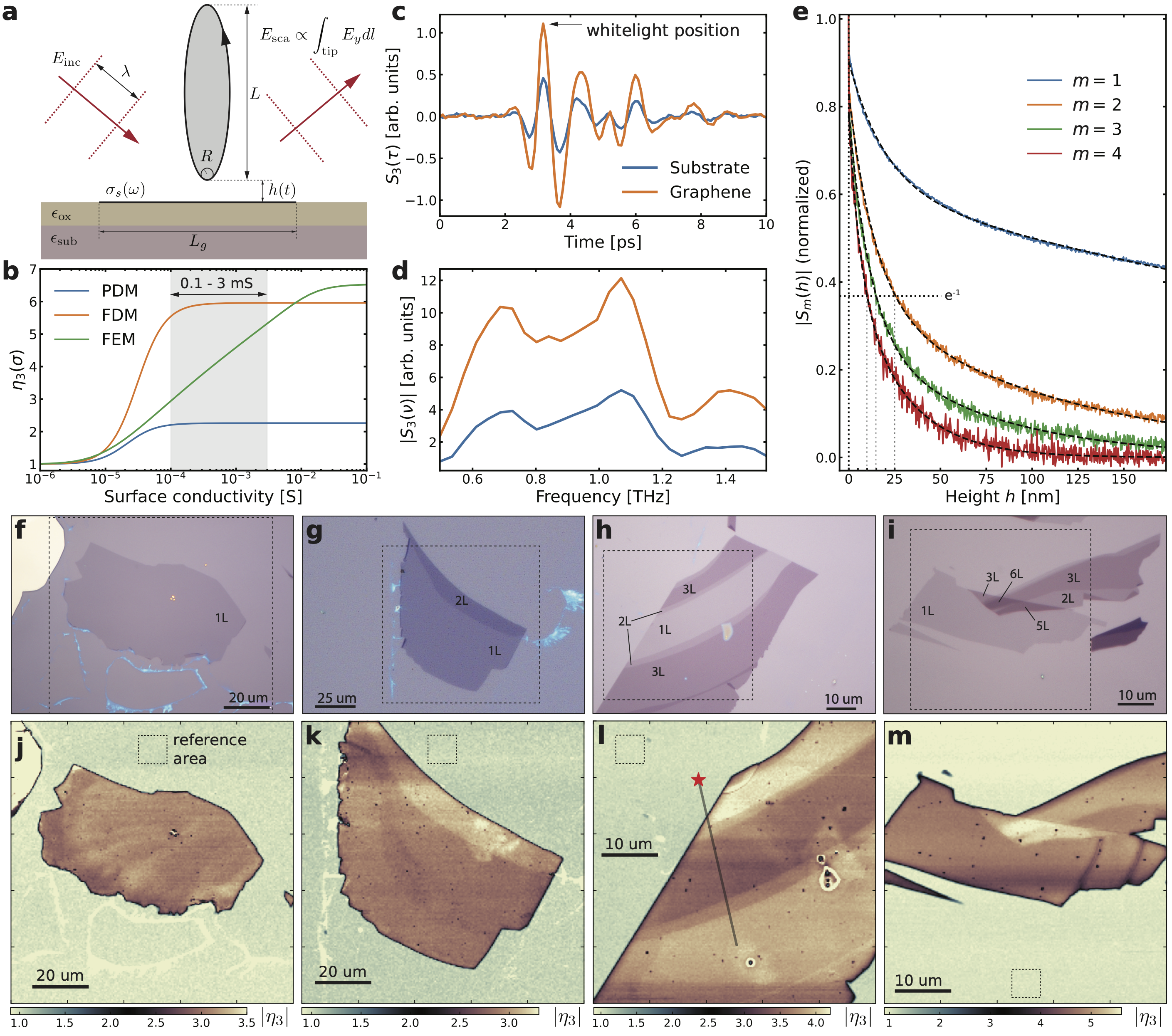
The THz-SNOM signal is recorded with the AFM operating in tapping mode. We use demodulation of the real-time, periodic scattering signal and detect the overtones of the tapping frequency to suppress the dominant far-field background signal. We use the overtone in the results presented below. A time trace of a scattered THz signal is represented by , where is the time delay along the THz time axis. Figure 1c shows representative THz transients recorded on the substrate (blue curve) and on a graphene flake (orange curve), in this example displaying a contrast of approximately 2. The frequency spectra of the two signals are shown in Fig. 1d in the range 0.5 to 1.6 THz. We observe significant interference in the time traces and spectral shapes, most likely originating from a standing wave pattern on the AFM tip and shank [38, 39].
A full THz-SNOM imaging measurement requires recording the scattered signal at each position on a sample surface. In this case, full spectroscopic characterization of the surface across the spectral range of the system is possible. This can be a rather time-consuming procedure, so we perform what are known as white-light scans. This scan mode is implemented by operating the instrument at a delay time equivalent to the peak of the THz waveform, indicated by the arrow in Fig. 1c, while performing the surface scan. In this manner, the recorded image contains information on the average optical properties of the sample, weighted by the spectral amplitude of the THz signal across its bandwidth instead of a frequency-resolved image. For conductive samples, the optical conductivity across the low THz range ( where is the carrier scattering time) is not expected to change dramatically. Hence, a white-light scan acts as a frequency-averaged result that is a versatile two-dimensional representation of a full, three-dimensional hyperspectral data set.
A stronger scattering signal indicates a higher conductivity of the surface. Thus, imaging of a conductive surface with THz-SNOM gives information about the local optical conductivity in the THz range, with a resolution related to the radius of curvature of the AFM tip in use [40]. An indication of the resolution is shown in Fig. 1e, where the approach curves recorded at a position on a graphene flake are shown for the first four demodulation orders (). The decay length of the signals is 25, 15, and 10 nm for , respectively.
2.3 THz-SNOM on exfoliated graphene
Graphene samples were prepared as described in the Methods section. Exfoliated single-layer graphene on a standard SiO2/Si substrate under ambient conditions typically displays a carrier concentration of and a mobility . This carrier concentration corresponds to a Fermi energy of and the mobility corresponds to a carrier scattering time of , a mean free path of , and a DC conductivity [41, 42].
Figures 1f-i (middle row) show optical microscope images of the graphene samples investigated here. Figures 1j-m (bottom row) show the corresponding THz-SNOM white-light images, represented by the magnitude of the third harmonic of the tapping signal relative to that obtained over a reference area on the substrate, indicated by the black, dashed squares in each image.
Figures 1f,j show a monolayer (1L) graphene flake extending in an irregular shape that covers approximately , as identified in the optical microscope image. In the THz-SNOM white-light image (Fig. 1j), we see a contrast ratio between graphene and substrate of approximately 3 and a small defect in the central region of the flake. Importantly, we see well-defined local variations of the THz-SNOM scattering signal within the flake, visually resembling weathered geographical formations on a cartographic landmass, which could be attributed to the fact that no steps (beyond those outlined in the Methods section) to clean or homogenise the graphene (for example, annealing) were taken.
Figures 1g,k show an example of a graphene sample with a large monolayer region and a smaller two-layer (2L) region in the upper part of the monolithic flake. The corresponding THz-SNOM image shows clearly identifiable 2L and 1L regions with a 5-10% contrast. Moreover, we also observe local variations of the signal within these 1L and 2L regions, respectively.
Figures 1h,l show another example of a multilayer sample structure, with 1L, 2L, and three-layer (3L) coverage. These distinct regions are easily identifiable in the paired THz-SNOM images. The red star and the black line in Fig. 1l indicate the start and path of a 30 line scan where we recorded the THz time-domain waveform for each position, as discussed below. Finally, Figures 1i,m show an example of a graphene flake with regions ranging from 1L to 6L, each with distinct contrast in the THz-SNOM image.
In addition to the contrast between various layer structures and local variations of the scattering signal within each layered region, we also observed localised dark spots in the THz-SNOM images, most likely due to polymer residuals and impurities from the transfer process and the subsequent short-term storage in an ambient atmosphere.
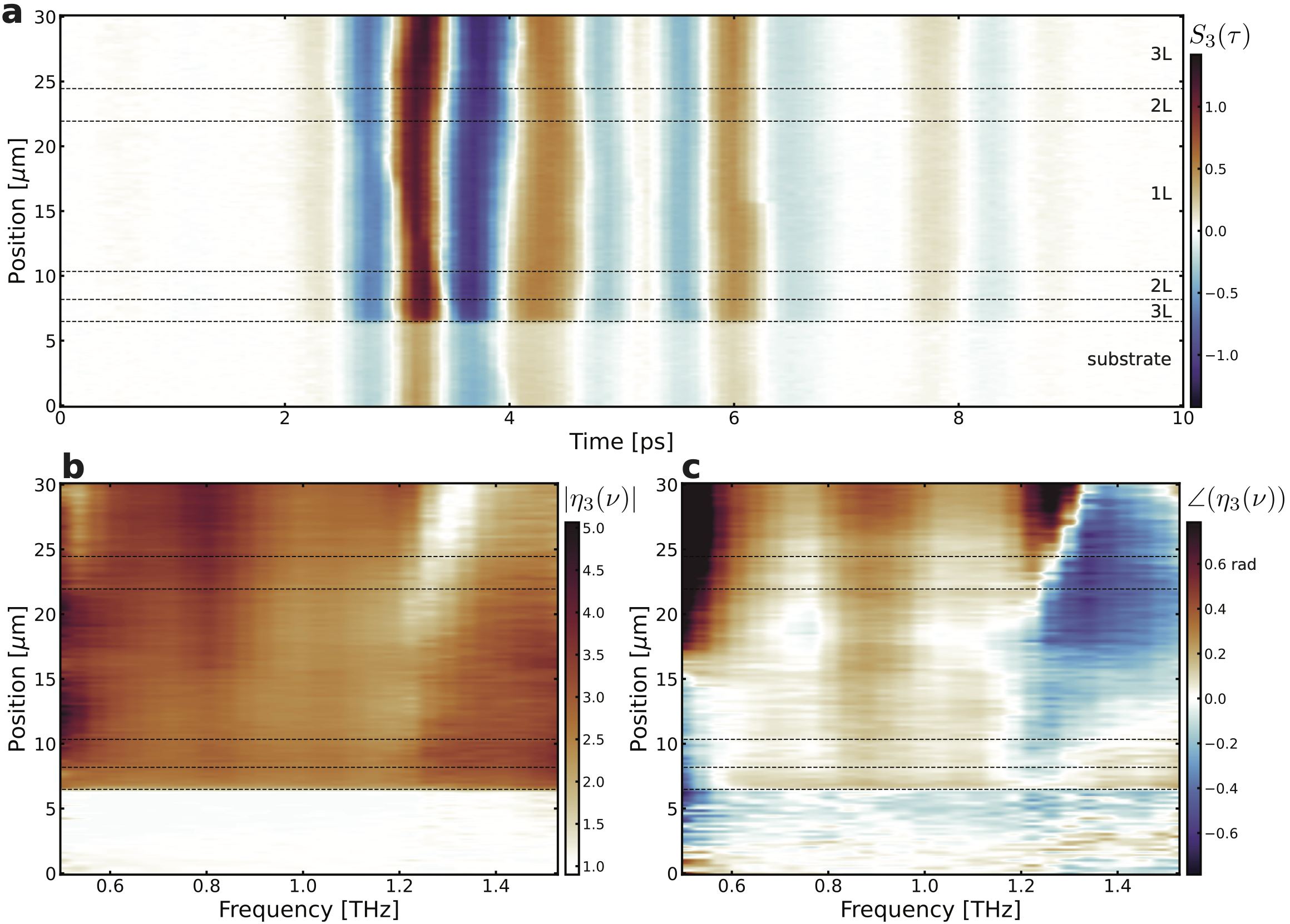
In addition to the white-light scans in Fig. 1, we performed a recording along the path indicated in Fig. 1l. The step size was 200 nm, and a full THz time-domain trace was recorded at each position. The reference was formed by the average of the first 10 time traces on the substrate. These time-domain traces are summarised in Fig. 2a, where the color coding indicates the detected amplitude of the third-order demodulated signal , where is the THz time delay. The horizontal dashed lines indicate the boundaries between the layers observed in the white-light scan. The signal increases significantly within the graphene area, but the boundaries between different layer counts are not visible. On the other hand, we observe a significant variation of the pulse shape along the line scan, visible as a slight drift and breathing of the vertical traces of the signal. Figure 2b shows the spectral variation of the ratio of the scattered signal magnitude on graphene relative to the substrate (). Despite the expected relatively flat spectral response of the conductivity of graphene (see below), there is a significant structure in the spectrally resolved contrast. Figure 2c shows the associated variations in the spectral phase relative to that of the substrate.
The observation that the white-light scans (Fig. 1) show clear contrast variations as a function layer number and position, but that the contrast is not visible in the spectrally resolved line scan indicates that factors other than the local conductivity of graphene contribute to the detected signal. Due to the strong spectral variations of the signal we suspect that standing wave patterns on the AFM tip shaft and cantilever strongly interfere with the spectroscopic measurements. A simple estimate of the resonance frequency of a cantilever and tip of total length 280 in the experiment is given by . The geometry of the tip and the cantilever is more complicated than this simple estimate can account for, and a full three-dimensional simulation, including the support chip, the cantilever, and the shank would therefore be required to determine the influence of the tip shape on the scattered signal [39]. However, we observe an oscillation of the scattered signal with a spectral periodicity consistent with this estimated simple resonance criterion. Furthermore, we observe the modulation of the scattering ratio gradually increases as the tip is moved onto the graphene sample. This may be an indication that the effective far-field reflection coefficient increases as the tip moves onto the more conductive region of the sample, and that the standing wave pattern then forms more efficiently. Taking all these factors into account in a quantitative manner is exceedingly difficult, and unfortunately hinders truly quantitative nanoscale spectroscopy in the THz range with current tip technology.
2.4 Theory and simulation of THz-SNOM response
Based on typical mobility values reported for exfoliated graphene under ambient conditions (), we will use a Fermi energy of 0.1 eV and an electron scattering time of 50 fs in the following, unless otherwise noted.
In a THz-SNOM experiment, the strong localisation of the long-wavelength optical field under the tip leads to a large in-plane momentum of the THz field. Thus, the near-field interaction with a sample involves the exchange of this large momentum with the material. For a frequency of 1 THz, the free-space momentum of the electromagnetic field is , so the dominant in-plane wavenumber under a tip with is , thus almost three orders of magnitude larger than . This enormous mismatch between and in the THz range marks a prominent fundamental difference between s-SNOM in the infrared region and the lower part of the THz range ( THz). In the IR, the mismatch between the far-field and near-field in-plane momenta may instead be a factor of just 30 (the same estimate using a wavelength of 1550 nm), so in that sense THz-SNOM is much deeper in the near-field regime than a corresponding IR-SNOM measurement. Hence, it is possible to enter deep into the regime of non-local response of 2D materials with THz-SNOM [43].
Momentum conservation leads to a shift in the Drude absorption weight in graphene from DC to a finite frequency , where is the Fermi velocity [44]. This effect is illustrated schematically in Fig. 3a,b. For a dominant in-plane momentum , the intraband transitions will peak at a frequency of approximately 3.2 THz. For a moderate electron scattering time , the mean free path of electrons in graphene is , comparable to the radius of the tip, and the locally enhanced electric field under the tip, therefore, varies on the length scale of . Local conductivity response models such as the Kubo formula [45] are based on a constant electric field. It is thus likely that the conductivity spectrum is influenced by non-local responses in the low-frequency range. Lovat et al. derived an analytical approximation of the non-local conductivity of graphene [46]. Figure 3c,d shows this analytical result calculated for the local and non-local conductivity of graphene at different Fermi energy levels (0-0.4 eV), showing the strong contrast between the local and non-local response in the low THz range. The relevant expressions are shown in the Supplementary Information.
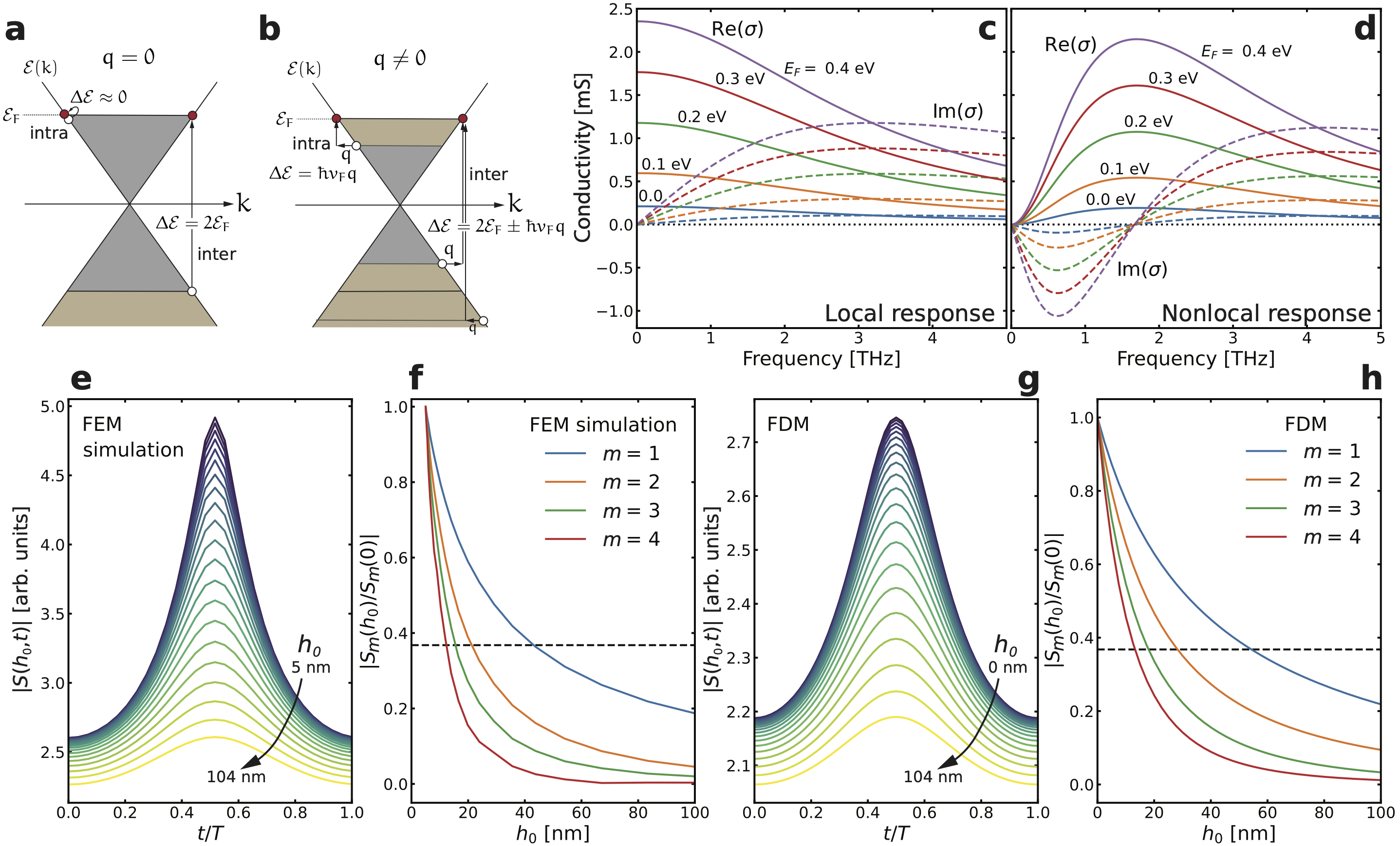
Figure 3e,f shows an example of a FEM simulation run on a model system with monolayer graphene on a SiO2/Si substrate where a THz-SNOM approach curve is simulated for a tapping amplitude of 100 nm. The minimum height is varied between 5-100 nm in a logarithmic manner, and for each height, the tapping sequence was simulated at a frequency of 1 THz. Figure 3e shows the time-domain results of the scattering signal for the different initial heights (top curve: ). The harmonic orders of the Fourier decomposition of each curve are shown in Fig. 3f for demodulation orders . The typical behaviour of the THz-SNOM approach curves is observed, with a biexponential decay and decay length in the 45-15 nm range. Figure 3g,h shows the corresponding results using the analytical FDM. The results are comparable to those obtained in the FEM simulation but with a lower height variation in the time domain. The calculated approach curves display decay lengths similar to those obtained by the FEM simulation.
Figure 4 summarises a comparison between FEM simulations and the analytical FDM model and demonstrates that the FEM shows a significantly larger signal contrast than the FDM model. In Fig. 4a, we show the scattering ratio as a function of the THz frequency , which is the ratio of the demodulated scattering signal magnitudes (demodulation order ) with the s-SNOM tip over graphene relative to the SiO2/Si substrate. The curve shown in grey is the average value of the scattering ratio over the 0.2-2 THz range and shows a significant variation between values of 4 and 5.7 for Fermi energy levels 0.0-0.4 eV. For comparison, Fig. 4b,c shows the expected contrast calculated by the FDM with local and non-local conductivity response, respectively. Here the THz-SNOM contrast decreases slightly with increasing Fermi energy (local response) and increases steeply at the lowest Fermi energies, followed by a levelling off in the case of non-local response. In both cases, the contrast variation is low (-0.15 and +0.25 for a local and non-local response, respectively, in the 0.0-0.4 eV range of the Fermi energy.
Based on these fundamental results, we performed a spatially resolved FEM simulation on a monolayer graphene sheet (width 50 m) across the frequency range 0.2-2.0 THz, as shown in Fig. 4d. The colour map shows the frequency-resolved contrast magnitude , and the curve shown in grey is the frequency-averaged scattering ratio. The average scattering ratio is approximately 5, and the effect of the edges is seen as small modulations of the scattering signal. Figure 4e shows the result of a similar FEM simulation where the model graphene sample now consists of zones with 1, 2 and 3 layers (1L, 2L, and 3L). The conductivity of multilayer graphene is assumed to scale linearly with the number of layers (see Supplementary Information). As expected from single-point simulations, the simulated scattering contrast increases with the layer count. The average scattering ratio (curve shown in grey) shows a layer contrast of 1.05 and 1.17, respectively, when moving from 1 layer to 2 and 3 layers. Hence, the experimentally measurable contrast is also present in the FEM simulations. We also observe that the contrast depends on the position of the sample. In Fig. 4, the tip is illuminated by a plane-wave from the direction of negative positions to positive positions, and we find that the layer contrast is clearest in the sample’s top half (positive positions). This observation is likely due to interference with edge-launched plasmonic surface modes in graphene [47].
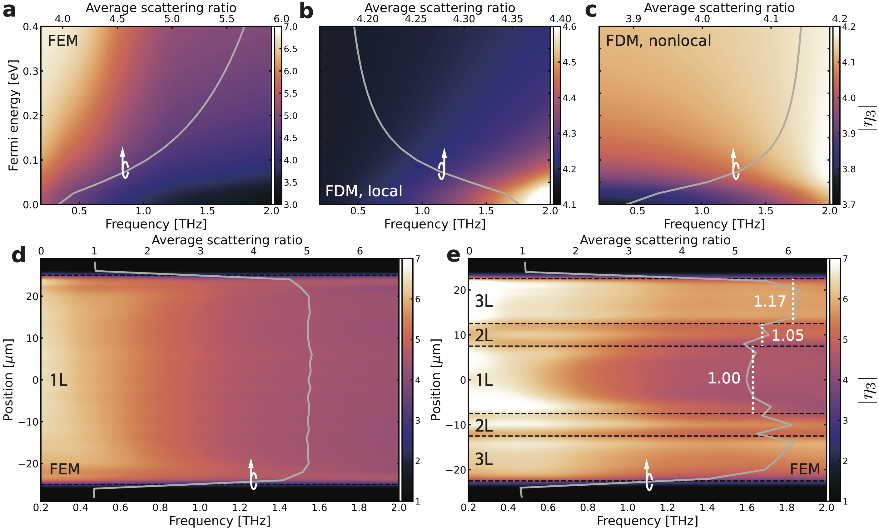
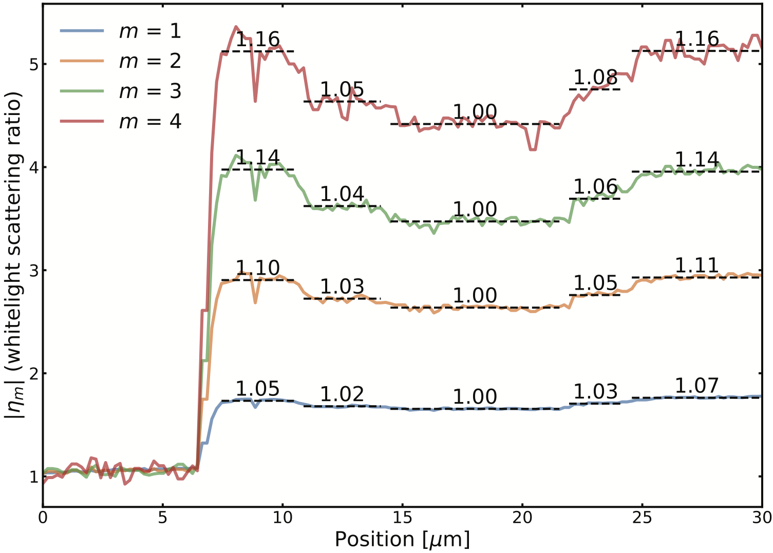
The simulated sample structure in Fig. 4 is similar to the line scan across one of the graphene samples, as shown in Fig. 1l. Hence, we can directly compare the experimentally observed contrast with the FEM results. This comparison is shown in Fig. 5. Here the experimental contrast along the line scan is shown, and we show the average scattering ratio relative to that obtained in the region of monolayer graphene (position 15-22 m). The first four demodulation orders () are shown. For , the experimental contrast with monolayer graphene is 1.04 (two layers) and 1.14 (three layers), comparable to the contrast observed in FEM simulations. It is tempting to directly compare the specific contrast values between the experiment and the FEM simulation. However, several factors hinder such a comparison. First, the assumption in the FEM simulation that the conductivity scales linearly with the layer count is oversimplified. Second, the absolute value of the contrast in the FEM simulation depends on a typical Fermi energy level of the graphene that has not been confirmed for our specific samples. However, the contrast comparison allows us to conclude that the experimental THz-SNOM contrast can be explained by the same effects included in the FEM simulation, namely the electromagnetic interaction in the local regime.
3 Methods
Sample Preparation
Graphene samples were prepared by mechanical exfoliation of graphite (NGS Naturgraphit GmbH) on silicon wafers with a 90 nm thick thermal SiO2 layer, resulting in a wide range of graphene flakes with various thicknesses distributed on the same substrate. Optical microscopy was then used to identify suitable monolayer and few-layer flakes on the surface, and to assess the number of graphene layers on a given sample based on the optical contrast [48, 49].
Experimental details and data extraction
THz-SNOM is performed with a commercial s-SNOM system (Attocube THz-NeaSCOPE) equipped with an integrated THz time-domain spectroscopy module (Attocube/Menlo Systems TeraSmart). THz pulses are generated and detected by photoconductive antennas, and the integrated system has a useful signal-to-noise ratio in the frequency band 0.5–2 THz. The system operates as an atomic force microscope (AFM), with optical access to the AFM tip. The THz beam is guided and focused via reflective optics onto the AFM tip, and identical optics guide the scattered THz light from the AFM tip to the detector. We used solid PtIr AFM tips with a tip shank length of (Rocky Mountain Nanotechnology, 25PtIr200B-H). We operated the THz-SNOM system in an atmosphere purged with nitrogen (N2) gas to minimise water vapour absorption lines in the detected THz spectra. A schematic of the AFM tip on a sample with the incident and scattered THz radiation is shown in Fig. 1a.
The THz-SNOM signal is recorded with the AFM operating in tapping mode, as is standard in most modern SNOM systems. Briefly, the time-dependent scattered signal is detected in real-time and demodulated at the overtones of the tapping frequency to suppress the far-field background signal. Here is the demodulation order, typically . Therefore, a time trace of a scattered THz signal is represented as , where is the time delay along the THz time axis, as shown in Fig. 1b. The frequency spectra of these two signals are shown in Fig. 1c, covering the 0.5–1.6 THz range.
FEM Simulations
In the finite-element modelling (FEM) of the tip-sample interaction we represent the scattered THz signal as the integrated -component of the electric field on the surface of the AFM tip, as indicated in Fig. 1a. We used the commercial software COMSOL Multiphysics to simulate the electromagnetic scattering of THz fields from the AFM tip in the THz-SNOM experiment. Following the methods described by Conrad et al. [37], we simplified the simulation domain to 2D, allowing a sufficiently fine meshing for accurate representation of the scattered field, and to support extended parameter sweeps of spectrally and spatially resolved simulations.
Graphene was modelled as an infinitely thin transition layer with intraband sheet conductivity described by the Kubo formalism, as detailed in the Supplementary Information. Multilayer graphene was, for simplicity, modelled as . Although simple, this representation is in reasonable agreement with the overall trend observed in DC conductivity measurements on multilayer samples [50]. We included a layer of SiO2 (thickness 90 nm, ) on top of the Si substrate (). For the main simulations, the tip was modelled as an ellipsoid with a major semi-axis length of m (total tip length ), radius of curvature of , and the resulting minor semi-axis length . Supplementary information shows additional simulation results with variations of and .
The simulation domain was surrounded by scattering boundary conditions, and excited in the frequency domain by a plane wave incident from the top left at an angle of 30 degrees from vertical. We used incident frequencies between 0.2 and 2 THz in the simulations.
On average, the meshing process resulted in approximately cells adaptively distributed over the simulation area of . Further details are given in the Supplementary Information.
4 Conclusion
We have shown that despite theoretical models predicting a lack of contrast in highly conducting samples and notable supporting experiments, THz-SNOM can in fact detect small variations in the local conductivity of graphene samples, not only enabling the differentiation of the number of graphene layers in a multilayer sample but even enabling detailed inspection of the local variations of the conductivity within monolayer graphene samples. The observed contrast cannot be explained by the finite dipole model, although the inclusion of the nonlocal response of graphene enabled the FDM to predict the experimentally observed trend of higher contrast with higher conductivity of graphene. On the other hand, the observed contrast could almost be quantitatively reproduced by a simple finite-element simulation without nonlocal effects. This shows that the unexpected contrast is rooted in a classical electromagnetic interaction and suggests that the FDM can be expanded to consider thin layers of high, finite conductivity.
Our work strongly suggests that spectrally resolved THz-SNOM can—contrary to expectations—be a powerful tool for quantitative measurements of the conductivity spectrum and, therefore, for determining both the DC conductivity and the scattering rate of conductive 2D materials and thin () films of metals. Uniquely, this information can be extracted at a scale that is smaller or comparable with the transport lengths, such as the mean free path or coherence length. THz-SNOM will be invaluable for unravelling local transport properties in quantum materials and systems, including correlated conductors, topological materials, twisttronics, straintronics, and spintronics, just as it could be highly suitable for optimisation and process development of 2D materials within a commercial context. Future improvements in tip design that suppress standing waves on the cantilever and shank would further enable the application of spectroscopic THz-SNOM to investigate conductive surfaces at the nanoscale.
Supplementary information
Supplementary information available.
Acknowledgements
We thank Martijn Wubs, Nicolas Stenger and N. Asger Mortensen for valuable discussions on non-local response in electrodynamics. We acknowledge partial financial support from the Danish Independent Research Fund (projects ULTRA-TED, ULTRA-LOWD, and Tr2DEO), the NNF Challenge Program BIOMAG, the Villum Foundation (IonGate), and the Carlsberg Foundation (DEEP-MAP).
Appendix S1 Supplementary information
Supplementary information on local and nonlocal conductivity models, experimental THz-SNOM results on graphene, reproducibility of results, and simulation details.
S1.1 Local and nonlocal conductivity of graphene
Using the Kubo formalism, the intraband conductivity of graphene in the local limit can be written as [51]
| (S1) |
where is the Fermi energy, is the electron scattering time, is the temperature, and is the Boltzmann constant.
In a THz-SNOM experiment the strong localization of the long-wavelength optical field under the tip leads to a large in-plane momentum of the THz field. Thus, the near-field interaction with a sample involves exchange of this large momentum with the material.
The relevant value of is determined by the localization of the electric field under the tip, which in turn is determined by the radius of curvature of the tip so that , which for a 50-nm radius of curvature gives . Within the framework of the point dipole model (see below), the dominant in-plane momentum can be calculated as the maximum of the weight function averaged over a tapping cycle [52],
| (S2) |
where is the modified Bessel function of the first kind of real order. For a tapping amplitude and a tip radius the weight function peaks at , in reasonable agreement with the simpler estimate .
Lovat et al. [46] developed a semiclassical model for the nonlocal intraband transverse and longitudinal conductivity of graphene with a convenient closed-form formulation, derived from the semiclassical Boltzmann transport equation under the Bhatnagar-Gross-Krook (bgk) model [53] that, as the Mermin correction [54] to the Lindhard model, assures local charge conservation.
| (S3) | |||||
| (S4) | |||||
| (S5) | |||||
| (S6) | |||||
| (S7) | |||||
| (S8) |
In the local limit () the Lovat model reduces to the Kubo formula, Eq. (S1).
S1.2 THz-SNOM: Finite dipole model
The finite dipole model (FDM) [27, 55] is an electrostatic model that describes the polarizability of a spheroidal, metallic tip close to a surface. The FDM takes a finite size of the tip into account and thus extends the point dipole model (PDM) [26, 9]. In both the FDM and the PDM, the scattered electric field from the dipole representing the tip-surface system is
| (S9) |
where is the incident electric field, is the effective polarizability of the tip-sample system. The prefactor is the far-field Fresnel reflection factor taking specular reflection of the incident and scattered fields into account. The tip extends in the vertical () direction, scattering the component of the electric field, corresponding to polarization.
Following the notation used by Hauer et al. [56], the effective polarizability is in the FDM defined by the near-field (quasi-electrostatic) reflection coefficient and two geometric function and ,
| (S10) | |||||
| (S11) |
Here is an empirical factor [27, 55], is the radius of curvature of the tip, is the height from the sample surface to the tip, and are the approximate positions of the point charge representing a fictual point monopole and a near-field induced monopole , and is the half of the length of the spheroidal dipole. Table 1 summarizes the parameters used in our FDM calculations.
| Parameter | Value |
|---|---|
| 600 nm | |
| 50 nm | |
| 0.7 | |
| 100 nm | |
| 83 kHz |
The scattered field contains both far-field and near-field information. The far-field contribution can be effectively suppressed by tapping of the tip at some frequency and detection of the scattered signal at a higher harmonic . The height over the surface of the tip is modulated as , and the harmonic orders of the scattered signal is recovered by Fourier decomposition of the time-dependent signal,
| (S12) |
where is the tapping period.
The near-field reflection coefficient is, for an infinite, homogeneous substrate with relative permittivity , given by . This relation is the electrostatic version of the Fresnel reflection coefficient for -polarized electric fields and is derived in the limit of infinite in-plane momentum of the electric field. In the quasi-electrostatic case where the frequency of the electromagnetic field is low but nonzero, and the substrate under the tip is covered by an infinitely thin conductive film with (possibly nonlocal) sheet conductance the expression is replaced by a more general [52],
| (S13) |
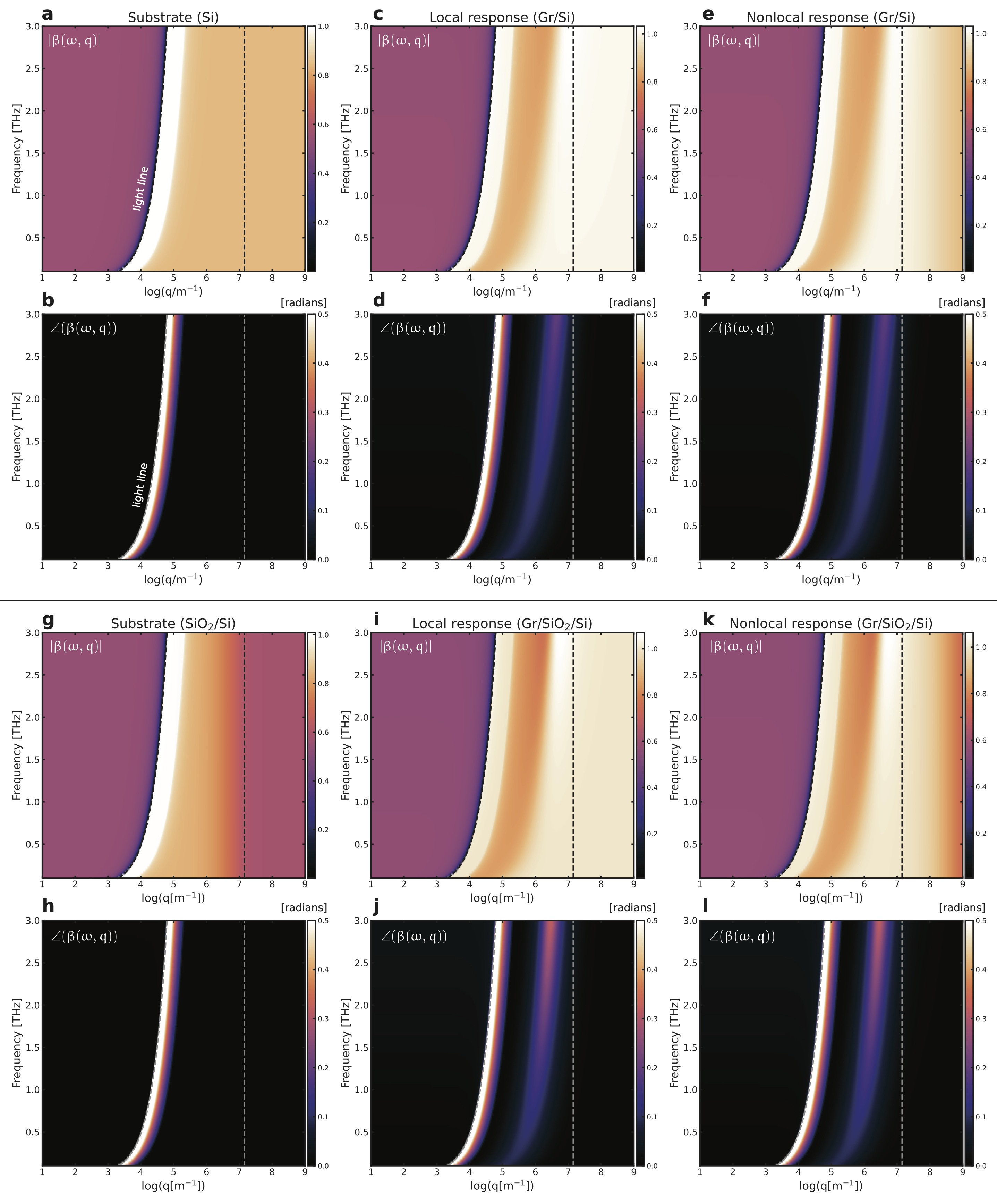
In the experiments presented in this paper, the graphene samples are deposited on an SiO2/Si substrate, with 90 nm thickness of the SiO2 layer. We, therefore, need to incorporate the thin oxide layer in the modeling of the near-field reflection coefficient. We follow the matrix-based method first described by Zhan et al. [57] and later by Wirth et al. [34] where the reflection from a layered sample is modeled by matrices representing each interface and layer in the stack.
The matrices and are the transfer matrices for -polarized light across the interface between air and SiO2 and the SiO2/Si interface, respectively,
| (S14) |
Here is the out-of-plane wave number in medium and is the permittivity of medium (: air, : SiO2, : Si).
The propagation matrix through the SiO2 spacer layer of thickness is
| (S15) |
The full transfer matrix of the layered structure is then . For a conductive film directly on a semi-infinite substrate, . In both cases the near-field reflection coefficient is then extracted from the elements of ,
| (S16) |
Figure S6 plots for two geometries. The two top rows are calculated for graphene deposited directly on a silicon substrate (two media, ), and the bottom two rows are calculated for graphene on a SiO2/Si structure (three media, ). Rows 1,3 show the amplitude, and rows 2,4 show the phase of . The left column shows for the substrate without graphene film, the center column shows using the local conductivity of graphene, and the right column is calculated using the nonlocal response of graphene. Graphene is represented by a Fermi energy of 0.1 eV, a scattering time of 50 fs, and a temperature of 300 K. The vertical dashed line in all plots shows the dominant in-plane momentum for a tip radius of curvature of 50 nm and a tapping amplitude of 100 nm (see Eq. (S2)). The dashed curves show the light line ().
S1.3 FEM simulations
We use the commercial software COMSOL Multiphysics to simulate the electromagnetic scattering of THz fields from the AFM tip in the THz-SNOM experiment. Following the methods described by Conrad et al. [37], we simplify the simulation to 2D. This enables sufficiently fine meshing and the extended parameter sweeps required for broadband, spatially resolved simulations of the experiments.
Graphene was modeled as an infinitely thin transition layer with sheet intraband sheet conductivity given by Eq. (S1). Multilayer graphene was, for simplicity and the lack of a more precise representation, modeled as . While this representation is a stark simplification, it agrees reasonably with the overall trend observed with DC conductivity measurements on multilayer samples [50]. We included a SiO2 layer (thickness 90 nm, ) on top of the Si substrate (). The tip was modeled as a spheroidal shape with a major semiaxis length of m, a radius of curvature of , and resulting minor semiaxis length . The tip material was modeled as a Drude metal with the finite conductivity of a typical good conductor.
The simulation domain was surrounded by scattering boundary conditions and excited in the frequency domain by a plane wave incident from the top left at an angle of 30 degrees from vertical. We used incident frequencies between 0.2 and 2 THz in the simulations.
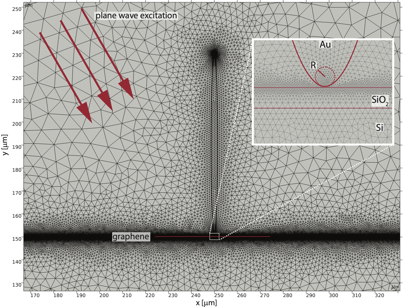
The meshing on average included approximately cells adaptively meshed over the simulation area of , as illustrated in Fig. S7. The inset shows the meshing near the tip apex for the smallest tip-surface distance of 5 nm used in the simulation runs.
A simulation run consisted of individual simulations for 16 different tip heights over the sample according to the formula . We simulated half of the oscillation cycle of the tip. We used a tapping amplitude and a minimum height . After each simulation, the scattered signal was calculated as the component of the electric field integrated over the full surface of the spheroidal tip shape. The Fourier components of the sequence were then calculated and used as the final output of the simulation. Based on this scheme, sweeps over frequencies (0.2–2 THz), the Fermi energy of graphene (0–0.4 eV), and the lateral position of the graphene sheet on the surface could be performed.
A single calculation (one height , one frequency ) requires 10-15 s of simulation time, leading to a run time of approximately 200 s for the simulation of a full tapping cycle on a desktop computer (Intel i9-11900K, eight physical cores, 128GB memory).
In the main article, the calculated THz-SNOM contrast between graphene with a given conductivity and the substrate is shown for a tip length m in Fig. 1b. For this calculation, we have used a frequency and a freely varying conductivity as indicated in the figure () instead of the Drude-like conductivity model. In Fig. S8, we further detail the influence of the tip length on the graphene-substrate contrast in the FEM simulation. The figure shows the contrast as a function of the conductivity of the graphene, in the range , for tip lengths of 1.2 m, 20 m, and 80 m (major semi-axis lengths of 600 nm, 20 m, 40 m). The gray area of the plot indicates the typical conductivity range of conductivities of exfoliated and CVD-grown graphene under ambient conditions.
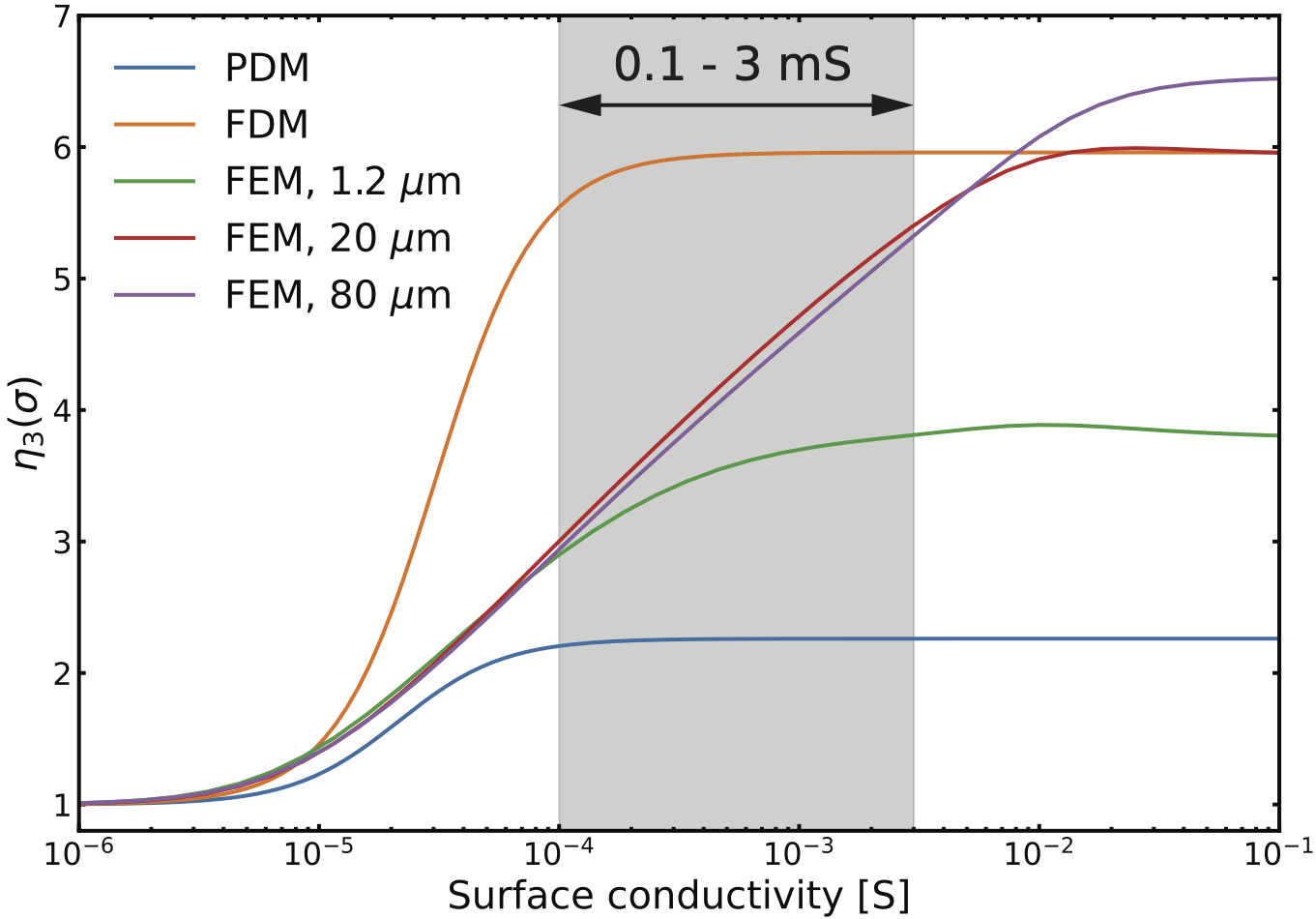
The longer tips (m and m) display similar contrasts between the graphene and the substrate, and the short tip ( m) shows a weaker contrast variation with conductivity. Hence, the FEM simulations indicate that for realistic tip lengths used in practice, the contrast variation with conductivity is only weakly dependent on the dimensions of the tip. We note that in the case of the FEM simulations, the absolute value of the contrast is not directly comparable with the contrast observed in experiments. The simulations are simplified to 2D, and the real shape of the full tip and cantilever is not considered.
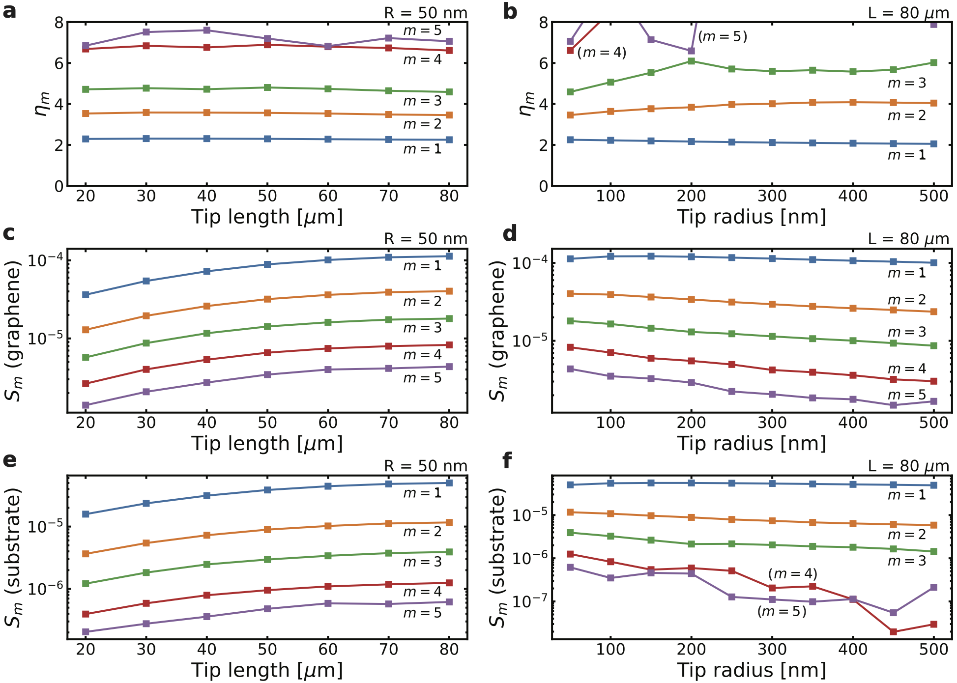
Figure S9 shows the results of simulations with varying tip length and tip radius. The graphene conductivity is 1 mS, and the frequency is 1 THz in the simulations. Figure S9a,b shows the scattering ratio (graphene/substrate) when the tip length is varied (Fig. S9a) and when the tip radius is varied (Fig. S9b). Data are shown for demodulation orders , with numerical noise influencing in Fig. S9b. It can be seen that the scattering ratio is rather constant in the parameter space investigated here. Figure S9c,e and S9d,f shows the scattering signals from graphene and substrate for the parameter sweeps, used to form the scattering ratios in Fig. S9a,b. Here the simulation predicts that a longer tip results in a larger absolute scattering signal, as could be expected. On the other hand, the absolute signal strength is reduced slightly for larger radii of the tip.
References
- \bibcommenthead
- Tomaino et al. [2011] Tomaino, J.L., Jameson, A.D., Kevek, J.W., Paul, M.J., Zande, A.M., Barton, R.A., McEuen, P.L., Minot, E.D., Lee, Y.S.: Terahertz imaging and spectroscopy of large-area single-layer graphene. Optics Express 19(1), 141–146 (2011) https://doi.org/10.1364/oe.19.000141
- Buron et al. [2012] Buron, J.D., Petersen, D.H., Bøggild, P., Cooke, D.G., Hilke, M., Sun, J., Whiteway, E., Nielsen, P.F., Hansen, O., Yurgens, A., Jepsen, P.U.: Graphene conductance uniformity mapping. Nano Letters 12(10), 5074–5081 (2012) https://doi.org/10.1021/nl301551a
- Bøggild et al. [2017] Bøggild, P., Mackenzie, D.M.A., Whelan, P.R., Petersen, D.H., Buron, J.D., Zurutuza, A., Gallop, J., Hao, L., Jepsen, P.U.: Mapping the electrical properties of large-area graphene. 2D Materials 4(4), 042003 (2017) https://doi.org/10.1088/2053-1583/aa8683
- Whelan et al. [2021] Whelan, P.R., Zhou, B., Bezencenet, O., Shivayogimath, A., Mishra, N., Shen, Q., Jessen, B.S., Pasternak, I., Mackenzie, D.M.A., Ji, J., Cunzhi, S., Seneor, P., Dlubak, B., Luo, B., Østerberg, F., Huang, D., Shi, H., Luo, D., Wang, M., Ruoff, R.S., Conran, B., McAleese, C., Huyghebaert, C., Brems, S., Booth, T., Napal, I., Strupinskii, W., Petersen, D.H., Forti, S., Coletti, C., Jouvray, A., Teo, K.B.K., Centeno, A., Zurutuza, A., Legagneux, P., Jepsen, P.U., Bøggild, P.: Case studies of electrical characterisation of graphene by terahertz time-domain spectroscopy. 2D Materials 8, 022003 (2021) https://doi.org/10.1088/2053-1583/abdbcb
- Pohl et al. [1984] Pohl, D.W., Denk, W., Lanz, M.: Optical stethoscopy: Image recording with resolution /20. Applied Physics Letters 44(7), 651–653 (1984) https://doi.org/10.1063/1.94865
- Zenhausern et al. [1994] Zenhausern, F., O’Boyle, M.P., Wickramasinghe, H.K.: Apertureless near‐field optical microscope. Applied Physics Letters 65(13), 1623–1625 (1994) https://doi.org/10.1063/1.112931
- Keilmann et al. [1996] Keilmann, F., Weide, D.W., Eickelkamp, T., Merz, R., Stöckle, D.: Extreme sub-wavelength resolution with a scanning radio-frequency transmission microscope. Optics Communications 129(1–2), 15–18 (1996) https://doi.org/10.1016/0030-4018(96)00108-3
- Knoll et al. [1997] Knoll, B., Keilmann, F., Kramer, A., Guckenberger, R.: Contrast of microwave near-field microscopy. Applied Physics Letters 70(20), 2667–2669 (1997) https://doi.org/10.1063/1.119255
- Knoll and Keilmann [2000] Knoll, B., Keilmann, F.: Enhanced dielectric contrast in scattering-type scanning near-field optical microscopy. Optics Communications 182(4), 321–328 (2000) https://doi.org/10.1016/S0030-4018(00)00826-9
- Liewald et al. [2018] Liewald, C., Mastel, S., Hesler, J., Huber, A.J., Hillenbrand, R., Keilmann, F.: All-electronic terahertz nanoscopy. Optica 5(2), 159–163 (2018) https://doi.org/10.1364/OPTICA.5.000159
- Chen et al. [2020] Chen, X., Liu, X., Guo, X., Chen, S., Hu, H., Nikulina, E., Ye, X., Yao, Z., Bechtel, H.A., Martin, M.C., Carr, G.L., Dai, Q., Zhuang, S., Hu, Q., Zhu, Y., Hillenbrand, R., Liu, M., You, G.: Thz near-field imaging of extreme subwavelength metal structures. ACS Photonics 7(3), 687–694 (2020) https://doi.org/10.1021/acsphotonics.9b01534
- Wiecha et al. [2021] Wiecha, M.M., Kapoor, R., Roskos, H.G.: Terahertz scattering-type near-field microscopy quantitatively determines the conductivity and charge carrier density of optically doped and impurity-doped silicon. APL Photonics 6(12), 126108 (2021) https://doi.org/10.1063/5.0070608
- Schäffer et al. [2023] Schäffer, S., Ogolla, C.O., Loth, Y., Haeger, T., Kreusel, C., Runkel, M., Riedl, T., Butz, B., Wigger, A.K., Bolívar, P.H.: Imaging the terahertz nanoscale conductivity of polycrystalline CsPbBr3 perovskite thin films. Nano Letters (2023) https://doi.org/10.1021/acs.nanolett.2c03214
- Chen et al. [2020] Chen, X., Liu, X., Guo, X., Chen, S., Hu, H., Nikulina, E., Ye, X., Yao, Z., Bechtel, H.A., Martin, M.C., Carr, G.L., Dai, Q., Zhuang, S., Hu, Q., Zhu, Y., Hillenbrand, R., Liu, M., You, G.: THz near-field imaging of extreme subwavelength metal structures. ACS Photonics 7(3), 687–694 (2020) https://doi.org/10.1021/acsphotonics.9b01534
- Chen et al. [2022] Chen, S., Bylinkin, A., Wang, Z., Schnell, M., Chandan, G., Li, P., Nikitin, A.Y., Law, S., Hillenbrand, R.: Real-space nanoimaging of THz polaritons in the topological insulator Bi2Se3. Nature Communications 13(1), 1374 (2022) https://doi.org/%****␣THz-SNOM_main_article.bbl␣Line␣375␣****10.1038/s41467-022-28791-x
- Kuschewski et al. [2016] Kuschewski, F., Ribbeck, H.-G.v., Döring, J., Winnerl, S., Eng, L.M., Kehr, S.C.: Narrow-band near-field nanoscopy in the spectral range from 1.3 to 8.5 THz. Applied Physics Letters 108(11), 113102 (2016) https://doi.org/10.1063/1.4943793
- Jepsen et al. [2011] Jepsen, P.U., Cooke, D.G., Koch, M.: Terahertz spectroscopy and imaging – modern techniques and applications. Laser & Photonics Reviews 5(1), 124–166 (2011) https://doi.org/10.1002/lpor.201000011
- Moon et al. [2015] Moon, K., Park, H., Kim, J., Do, Y., Lee, S., Lee, G., Kang, H., Han, H.: Subsurface nanoimaging by broadband terahertz pulse near-field microscopy. Nano Letters 15(1), 549–552 (2015) https://doi.org/10.1021/nl503998v
- Zhang et al. [2018] Zhang, J., Chen, X., Mills, S., Ciavatti, T., Yao, Z., Mescall, R., Hu, H., Semenenko, V., Fei, Z., Li, H., Perebeinos, V., Tao, H., Dai, Q., Du, X., Liu, M.: Terahertz nanoimaging of graphene. ACS Photonics 5(7), 2645–2651 (2018) https://doi.org/10.1021/acsphotonics.8b00190
- Aghamiri et al. [2019] Aghamiri, N.A., Huth, F., Huber, A.J., Fali, A., Hillenbrand, R., Abate, Y.: Hyperspectral time-domain terahertz nano-imaging. Optics Express 27(17), 24231–24242 (2019) https://doi.org/10.1364/OE.27.024231
- Kim et al. [2021] Kim, R.H.J., Huang, C., Luan, Y., Wang, L.-L., Liu, Z., Park, J.-M., Luo, L., Lozano, P.M., Gu, G., Turan, D., Yardimci, N.T., Jarrahi, M., Perakis, I.E., Fei, Z., Li, Q., Wang, J.: Terahertz nano-imaging of electronic strip heterogeneity in a dirac semimetal. ACS Photonics 8(7), 1873–1880 (2021) https://doi.org/10.1021/acsphotonics.1c00216
- Plankl et al. [2021] Plankl, M., Faria Junior, P.E., Mooshammer, F., Siday, T., Zizlsperger, M., Sandner, F., Schiegl, F., Maier, S., Huber, M.A., Gmitra, M., Fabian, J., Boland, J.L., Cocker, T.L., Huber, R.: Subcycle contact-free nanoscopy of ultrafast interlayer transport in atomically thin heterostructures. Nature Photonics (2021) https://doi.org/10.1038/s41566-021-00813-y
- Jing et al. [2021] Jing, R., Shao, Y., Fei, Z., Lo, C.F.B., Vitalone, R.A., Ruta, F.L., Staunton, J., Zheng, W.J.C., McLeod, A.S., Sun, Z., Jiang, B.-y., Chen, X., Fogler, M.M., Millis, A.J., Liu, M., Cobden, D.H., Xu, X., Basov, D.N.: Terahertz response of monolayer and few-layer WTe2 at the nanoscale. Nature Communications 12(1), 5594 (2021) https://doi.org/10.1038/s41467-021-23933-z
- Pizzuto et al. [2021] Pizzuto, A., Chen, X., Hu, H., Dai, Q., Liu, M., Mittleman, D.M.: Anomalous contrast in broadband thz near-field imaging of gold microstructures. Optics Express 29(10), 15190–15198 (2021) https://doi.org/10.1364/OE.423528
- Yao et al. [2019] Yao, Z., Semenenko, V., Zhang, J., Mills, S., Zhao, X., Chen, X., Hu, H., Mescall, R., Ciavatti, T., March, S., Bank, S.R., Tao, T.H., Zhang, X., Perebeinos, V., Dai, Q., Du, X., Liu, M.: Photo-induced terahertz near-field dynamics of graphene/InAs heterostructures. Optics Express 27(10), 13611–13623 (2019) https://doi.org/10.1364/OE.27.013611
- Knoll and Keilmann [1999] Knoll, B., Keilmann, F.: Near-field probing of vibrational absorption for chemical microscopy. Nature 399(6732), 134–137 (1999) https://doi.org/10.1038/20154
- Cvitkovic et al. [2007] Cvitkovic, A., Ocelic, N., Hillenbrand, R.: Analytical model for quantitative prediction of material contrasts in scattering-type near-field optical microscopy. Optics Express 15(14), 8550–8565 (2007) https://doi.org/10.1364/OE.15.008550
- McLeod et al. [2014] McLeod, A.S., Kelly, P., Goldflam, M.D., Gainsforth, Z., Westphal, A.J., Dominguez, G., Thiemens, M.H., Fogler, M.M., Basov, D.N.: Model for quantitative tip-enhanced spectroscopy and the extraction of nanoscale-resolved optical constants. Physical Review B 90(8), 085136 (2014) https://doi.org/10.1103/PhysRevB.90.085136
- Mester et al. [2022] Mester, L., Govyadinov, A.A., Hillenbrand, R.: High-fidelity nano-ftir spectroscopy by on-pixel normalization of signal harmonics. Nanophotonics 11(2), 377–390 (2022) https://doi.org/10.1515/nanoph-2021-0565
- Taubner et al. [2004] Taubner, T., Hillenbrand, R., Keilmann, F.: Nanoscale polymer recognition by spectral signature in scattering infrared near-field microscopy. Applied Physics Letters 85(21), 5064–5066 (2004) https://doi.org/10.1063/1.1827334
- Brehm et al. [2006] Brehm, M., Taubner, T., Hillenbrand, R., Keilmann, F.: Infrared spectroscopic mapping of single nanoparticles and viruses at nanoscale resolution. Nano Letters 6(7), 1307–1310 (2006) https://doi.org/10.1021/nl0610836
- Zhang et al. [2012] Zhang, L.M., Andreev, G.O., Fei, Z., McLeod, A.S., Dominguez, G., Thiemens, M., Castro-Neto, A.H., Basov, D.N., Fogler, M.M.: Near-field spectroscopy of silicon dioxide thin films. Physical Review B - Condensed Matter and Materials Physics 85 (2012) https://doi.org/10.1103/PhysRevB.85.075419
- Govyadinov et al. [2014] Govyadinov, A.A., Mastel, S., Golmar, F., Chuvilin, A., Carney, P.S., Hillenbrand, R.: Recovery of permittivity and depth from near-field data as a step toward infrared nanotomography. ACS Nano 8(7), 6911–6921 (2014) https://doi.org/%****␣THz-SNOM_main_article.bbl␣Line␣750␣****10.1021/nn5016314
- Wirth et al. [2021] Wirth, K.G., Linnenbank, H., Steinle, T., Banszerus, L., Icking, E., Stampfer, C., Giessen, H., Taubner, T.: Tunable s-SNOM for nanoscale infrared optical measurement of electronic properties of bilayer graphene. ACS Photonics 8(2), 418–423 (2021) https://doi.org/10.1021/acsphotonics.0c01442
- Fei et al. [2017] Fei, Z., Palomaki, T., Wu, S., Zhao, W., Cai, X., Sun, B., Nguyen, P., Finney, J., Xu, X., Cobden, D.H.: Edge conduction in monolayer WTe2. Nature Physics 13(7), 677–682 (2017) https://doi.org/10.1038/nphys4091
- Kim et al. [2015] Kim, D.-S., Kwon, H., Nikitin, A.Y., Ahn, S., Martín-Moreno, L., García-Vidal, F.J., Ryu, S., Min, H., Kim, Z.H.: Stacking structures of few-layer graphene revealed by phase-sensitive infrared nanoscopy. ACS Nano 9(7), 6765–6773 (2015) https://doi.org/10.1021/acsnano.5b02813
- Conrad et al. [2022] Conrad, G., Casper, C.B., Ritchie, E.T., Atkin, J.M.: Quantitative modeling of near-field interactions incorporating polaritonic and electrostatic effects. Optics Express 30(7), 11619–11632 (2022) https://doi.org/10.1364/OE.442305
- Mooshammer et al. [2020] Mooshammer, F., Huber, M.A., Sandner, F., Plankl, M., Zizlsperger, M., Huber, R.: Quantifying nanoscale electromagnetic fields in near-field microscopy by Fourier demodulation analysis. ACS Photonics 7(2), 344–351 (2020) https://doi.org/10.1021/acsphotonics.9b01533
- Mooshammer et al. [2021] Mooshammer, F., Plankl, M., Siday, T., Zizlsperger, M., Sandner, F., Vitalone, R., Jing, R., Huber, M.A., Basov, D.N., Huber, R.: Quantitative terahertz emission nanoscopy with multiresonant near-field probes. Optics Letters 46(15), 3572–3575 (2021) https://doi.org/10.1364/OL.430400
- Maissen et al. [2019] Maissen, C., Chen, S., Nikulina, E., Govyadinov, A., Hillenbrand, R.: Probes for ultrasensitive THz nanoscopy. ACS Photonics 6(5), 1279–1288 (2019) https://doi.org/10.1021/acsphotonics.9b00324
- Rumyantsev et al. [2010] Rumyantsev, S., Liu, G., Stillman, W., Shur, M., Balandin, A.A.: Electrical and noise characteristics of graphene field-effect transistors: ambient effects, noise sources and physical mechanisms. Journal of Physics: Condensed Matter 22(39), 395302 (2010) https://doi.org/10.1088/0953-8984/22/39/395302
- Gammelgaard et al. [2014] Gammelgaard, L., Caridad, J.M., Cagliani, A., Mackenzie, D.M.A., Petersen, D.H., Booth, T.J., Bøggild, P.: Graphene transport properties upon exposure to PMMA processing and heat treatments. 2D Materials 1(3), 035005 (2014) https://doi.org/10.1088/2053-1583/1/3/035005
- Lundeberg et al. [2017] Lundeberg, M.B., Gao, Y., Asgari, R., Tan, C., Van Duppen, B., Autore, M., Alonso-González, P., Woessner, A., Watanabe, K., Taniguchi, T., Hillenbrand, R., Hone, J., Polini, M., Koppens, F.H.L.: Tuning quantum nonlocal effects in graphene plasmonics. Science 357(6347), 187–191 (2017) https://doi.org/10.1126/science.aan2735
- Carbotte et al. [2012] Carbotte, J.P., LeBlanc, J.P.F., Nicol, E.J.: Emergence of plasmaronic structure in the near-field optical response of graphene. Physical Review B 85(20), 201411 (2012) https://doi.org/10.1103/PhysRevB.85.201411
- Abergel et al. [2010] Abergel, D.S.L., Apalkov, V., Berashevich, J., Ziegler, K., Chakraborty, T.: Properties of graphene: a theoretical perspective. Advances in Physics 59(4), 261–482 (2010) https://doi.org/10.1080/00018732.2010.487978
- Lovat et al. [2013] Lovat, G., Hanson, G.W., Araneo, R., Burghignoli, P.: Semiclassical spatially dispersive intraband conductivity tensor and quantum capacitance of graphene. Physical Review B 87(11), 115429 (2013) https://doi.org/10.1103/PhysRevB.87.115429
- Jablan et al. [2009] Jablan, M., Buljan, H., Soljačić, M.: Plasmonics in graphene at infrared frequencies. Physical Review B 80(24), 245435 (2009) https://doi.org/10.1103/PhysRevB.80.245435
- Casiraghi et al. [2007] Casiraghi, C., Hartschuh, A., Lidorikis, E., Qian, H., Harutyunyan, H., Gokus, T., Novoselov, K.S., Ferrari, A.C.: Rayleigh imaging of graphene and graphene layers. Nano Letters 7(9), 2711–2717 (2007) https://doi.org/10.1021/nl071168m
- Jessen et al. [2018] Jessen, B.S., Whelan, P.R., Mackenzie, D.M.A., Luo, B., Thomsen, J.D., Gammelgaard, L., Booth, T.J., Bøggild, P.: Quantitative optical mapping of two-dimensional materials. Scientific Reports 8(1), 6381 (2018) https://doi.org/10.1038/s41598-018-23922-1
- Liu et al. [2013] Liu, G., Rumyantsev, S., Shur, M.S., Balandin, A.A.: Origin of 1/f noise in graphene multilayers: Surface vs. volume. Applied Physics Letters 102(9), 093111 (2013) https://doi.org/10.1063/1.4794843
- Falkovsky [2008] Falkovsky, L.A.: Optical properties of graphene. Journal of Physics: Conference Series 129(1), 012004 (2008) https://doi.org/10.1088/1742-6596/129/1/012004
- Fei et al. [2011] Fei, Z., Andreev, G.O., Bao, W., Zhang, L.M., McLeod, A.S., Wang, C., Stewart, M.K., Zhao, Z., Dominguez, G., Thiemens, M., Fogler, M.M., Tauber, M.J., Castro-Neto, A.H., Lau, C.N., Keilmann, F., Basov, D.N.: Infrared nanoscopy of dirac plasmons at the graphene–sio2 interface. Nano Letters 11(11), 4701–4705 (2011) https://doi.org/10.1021/nl202362d
- Bhatnagar et al. [1954] Bhatnagar, P.L., Gross, E.P., Krook, M.: A model for collision processes in gases. i. small amplitude processes in charged and neutral one-component systems. Physical Review 94(3), 511–525 (1954) https://doi.org/10.1103/PhysRev.94.511
- Mermin [1970] Mermin, N.D.: Lindhard dielectric function in the relaxation-time approximation. Physical Review B 1(5), 2362–2363 (1970) https://doi.org/10.1103/physrevb.1.2362
- Ocelić [2007] Ocelić, N.: Quantitative near-field phonon-polariton spectroscopy. Thesis, Technische Universität München (2007)
- Hauer et al. [2012] Hauer, B., Engelhardt, A.P., Taubner, T.: Quasi-analytical model for scattering infrared near-field microscopy on layered systems. Optics Express 20(12), 13173–13188 (2012) https://doi.org/10.1364/OE.20.013173
- Zhan et al. [2013] Zhan, T., Shi, X., Dai, Y., Liu, X., Zi, J.: Transfer matrix method for optics in graphene layers. J. Phys.: Condens. Matter 25(21), 215301 (2013) https://doi.org/10.1088/0953-8984/25/21/215301