In-plane magnetic field-driven conductance modulations in topological insulator kinks
Abstract
We present low-temperature magnetoconductance measurements on Bi1.5Sb0.5Te1.8Se1.2 kinks with ribbon-shaped legs. The conductance displays a clear dependence on the in-plane magnetic field orientation. The conductance modulation is consistent with orbital effect-driven trapping of the topological surface states on different side facets of the legs of the kink, which affects their transmission across the kink. This magnetic field-driven trapping and conductance pattern can be explained with a semiclassical picture and is supported by quantum transport simulations. The interpretation is corroborated by varying the angle of the kink and analyzing the temperature dependence of the observed magnetoconductance pattern, indicating the importance of phase coherence along the cross section perimeter of the kink legs.
I Introduction
Three-dimensional topological insulators (3D TIs) are a class of materials in which strong spin-orbit coupling leads to a band inversion in the bulk electronic band structure [1, 2]. This in turn causes the appearance of gapless surface states protected by time-reversal symmetry. Topological insulators are particularly interesting for applications in topological quantum computer architectures [3, 4, 5, 6, 7]. These circuits typically consist of networks of topological insulator nanoribbons combined with superconducting electrodes [8, 9, 10, 11, 12, 13, 14]. In this context, the electronic transport behavior of nanoribbons as well as more complex structures such as kinks and junctions of nanoribbons is of high interest.
In nanoribbon structures the existence of topological surface states is revealed by magnetotransport measurements [15, 16, 17, 18, 19, 20, 21, 22]. Here, regular Aharonov-Bohm oscillations are observed when an axial magnetic field is applied, due to the presence of closed-loop surface states. The appearance of Aharonov-Bohm oscillations also confirms that the transport in the surface states is phase coherent with a phase-coherence length on the order of a few hundred nanometers [17, 18, 21, 22]. For three-dimensional topological insulators, the surface transport is often accompanied by a transport channel carried by bulk carriers due to intrinsic doping effects [23, 24]. In this respect, nanostructures offer an unique advantage as their surface-to-volume ratio increases and the bulk and surface conductance contributions can be disentangled in transport experiments. In 3D TI nanoribbon-based three-terminal junctions it has been shown experimentally that the conductance can be steered by applying an in-plane magnetic field [2]. This steering effect is attributed to the interplay between the phase-coherent transport in topological surface states and an orbital effect on the side facets of the nanoribbon. This causes electrons in the surface states to be trapped on the upper or lower surface of a nanoribbon, depending on the relative orientation of each nanoribbon leg with respect to the in-plane magnetic field.
Analogously to the effect of the in-plane field on the conductance in three-terminal junctions, the theoretical models also predict a -periodic change in the conductance of a 3D TI nanoribbon-based kink under rotation of an in-plane magnetic field [1]. To address this issue we have studied the low-temperature magnetotransport properties of quadternary Bi1.5Sb0.5Te1.8Se1.2 kinks with different angles between the input and output terminal. Quadternary materials have been show to suppress the bulk conductivity in previous studies [27, 28, 29].The devices were fabricated using a selective-area molecular beam epitaxy (MBE) approach. The modulation of the conductance was then measured as a function of the angle of the applied in-plane magnetic field with respect to the orientation of the device. The experimental results are interpreted on the basis of a semi-classical theoretical model and corresponding simulations [2].
II Methods
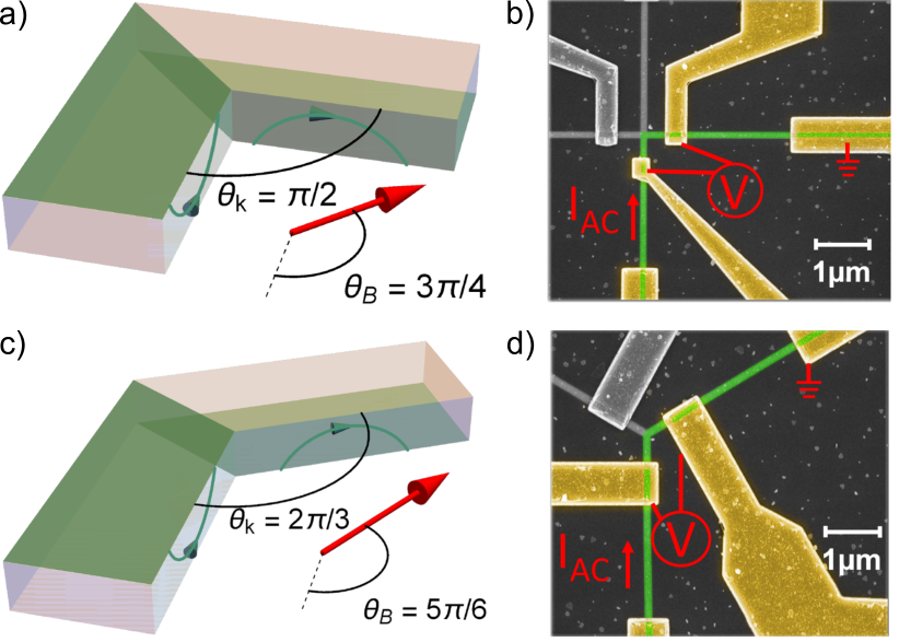
The Bi1.5Sb0.5Te1.8Se1.2 layer was grown by molecular beam epitaxy. A selective-area growth (SAE) approach was employed to yield the desired structures [30, 20, 31]. The samples were prepared in a 3 Step process. First, the substrate is prepared with a -thick-thermal SiO2 layer and a thick PECVD Si3N4 layer to form the selective-area growth mask. The shape of the SAE-trench was defined using reactive ion etching (CHF3/O2) and hydrofluoric acid wet etching after an electron beam lithography step. This is done in order to reveal the Si(111) surface as well as to passivate it before the growth. To prevent oxidation the film was capped using a 5-nm-thick AlOx layer. The kink structure are contacted with Ti contacts via ex-situ electron beam evaporation. Structures with a kink angle of and were investigated, which are part of a cross and symmetric 3-terminal structure, respectively. Figures 1 a) and c) show the corresponding schematic illustration of the kink structures together with the definitions of the kink and magnetic field angles , respectively. In Figs. 1 b) and d) scanning electron beam micrographs of the and the kink structure are shown.
From Hall measurements at 1.5 K we determined a carrier concentration of and a mobility of (see Supplementary Note 1 of Ref. [32]). The Ohmic contacts are formed by a thick Ti layer. Before deposition of the metal layer the AlOx capping in the contact areas was removed by wet chemical etching and argon sputtering.
The measurements were carried out in a variable temperature insert with a base temperature of . The conductance of the device was measured using a standard four-probe lock-in setup (cf. Figs. 1b) and d)). The rotation of the in-plane magnetic field with respect to the kink structure was realized by employing a mechanically rotatable sample rod, where the sample was rotated by in 19 steps. After each step the magnetic field was swept from to in order to realize an effective rotation of the magnetic field of .
The simulations of the conductance in the kink structures are based on a semiclassical theoretical model explained in detail in Ref. [2]. We consider a subband-quantized Dirac surface-state spectrum that is appropriate for the cross section geometry of the 3D TI kink legs and a Dirac point that is separated from the Fermi level by 0.1 eV.
III Magnetoconductance
Figure 2 a) shows the measured conductance in units of of the kink as a function of magnetic field, with and the electron charge and Planck’s constant. The measurements were taken at a temperature of . Each color coded line represents a single measurement in between to for a different in-plane magnetic field angle ranging from 0 to . The definition of the in-plane magnetic field angle with respect to the sample is given in Fig. 1 a).
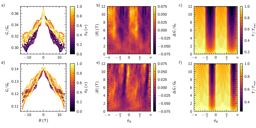
All magnetoconductance traces shown in Fig. 2 a) exhibit several prominent features. The conductance peak at zero magnetic field can be attributed to the weak antilocalization effect [33]. This peak structure has previously been observed in topological insulator nanoribbon structures [20]. It is due to electron interference after scattering on impurities in combination with the strong spin-orbit coupling of the material. The small fluctuations of the conductance over larger magnetic field intervals represent universal conductance fluctuations [34]. These are caused by the interference of a finite number of trajectories due to the small dimensions of the sample. Apart from these two features observed in each curve the color coded magnetic field sweeps also reveal a change in resistance with a change in the magnetic field angle . In order to analyzed the dependence of the magnetoconductance on the magnetic field orientation in detail, the data is plotted in the style of a color map as a function of the absolute magnetic field and the magnetic field angle . Here, we consider only the effective conductance change defined by
| (1) |
which is the normalized difference between the conductance at a certain magnetic field and in-plane field angle and the average conductance at constant magnetic field averaged over all angles . Figure 2 b) shows the effective conductance for the kink. A clear -periodic variation of the conductance with a variation of the in-plane magnetic field angle is visible. The areas of maximum and minimum conductance are centered around the values of , and , , respectively. The field orientation for the minimum conductance case is indicated in Fig. 1 a).
In the following, a kink with a larger angle between in and output terminal, i.e., a kink, is analysed. The corresponding normalized magnetoconductance as a function of magnetic field for in-plane angles between 0 and is shown in Fig. 2 d). Similar to the conductance of the kink a clear modulation of the conductance with the variation of the in-plane field angle can be seen. Analogous to the first device this data is converted to the effective conductance change using Eq. (1). Figure 2 e) shows the effective magnetoconductance of the kink. A shift of the position of the minimum and maximum conductance compared to measurements shown in Fig. 2 b) for the kink is observed. The experimentally observed modulations match well with the theoretically expected positions for maximum and minimum conductance, i.e. , and , , respectively. The positions are derived from trivial geometrical considerations regarding the aligned and transverse orientation of the magnetic field with respect to the kink-angle.
To explain the origin of the angle-modulated conductance pattern, we consider the impact of the orbital effect on the topological surface states in a semiclassical picture [2], analogous to the treatment of the steering effect in a topological insulator-based T-junction in Ref. [1]. On the top and bottom facets of the ribbon, the Lorentz force points perpendicular to the surface and can be neglected for surface-state motion that is bound to the surface of the ribbon. On the side facets (assumed to be perpendicular to the plane here), however, the Lorentz force induces a circular motion of the charge carriers (see Fig.1 a) and c)). Depending on the transverse velocity of the surface state, the carriers will be able to traverse the side facet from bottom to top (or vice versa) or not. Thus, when the transverse extent is smaller than the height of the ribbon, the carriers cannot traverse the side facet. For surface states that wrap phase-coherently around the perimeter of the ribbon cross section, it follows that the top or bottom surface effectively gets depleted, or, equivalently, carriers are trapped on the opposite surface. When the carriers on the two legs of the kink are trapped on opposite facets of the ribbon, the transmission across the kink is suppressed, as illustrated in Figs. 1 a) and c). This is also demonstrated by quantum transport simulations in the Supplementary Material of Ref. [2]. In Figs. 2 c) and f) the calculated normalized transmission as a function of magnetic field angle and absolute magnetic field are given for the kink and kink structures, respectively (see Supplementary Material for details). By comparing to Figs. 2 b) and e) one finds that the experimental results nicely follow the transmission pattern that results from the semiclassical picture. Comparing the simulations as well as the effective conductance color maps in Fig. 2 b) and e) it is clear that the range of angles with reduced conductance becomes narrower for an increased kink angle. This is consistent with the picture based on the Lorentz force, as the window of angles for which the Lorentz force has the opposite effect on the two legs of the kink (suppressing the transmission probability) naturally narrows down when the legs become more aligned.
In the Supplementary Material of Ref. [2], it was also shown that the steering effect is only expected for states that are located on the surface, and that the robustness of the effect against disorder is highly enhanced by spin-momentum locking, which suppresses scattering processes with a significant change in momentum. The observed magnetoconductance pattern is therefore not likely to originate from trivial bulk states or trivial surface states without spin-momentum locking. Hence, in-plane magnetic field dependence of the conductance across the kink structures provides a robust transport signature of topological surface states.
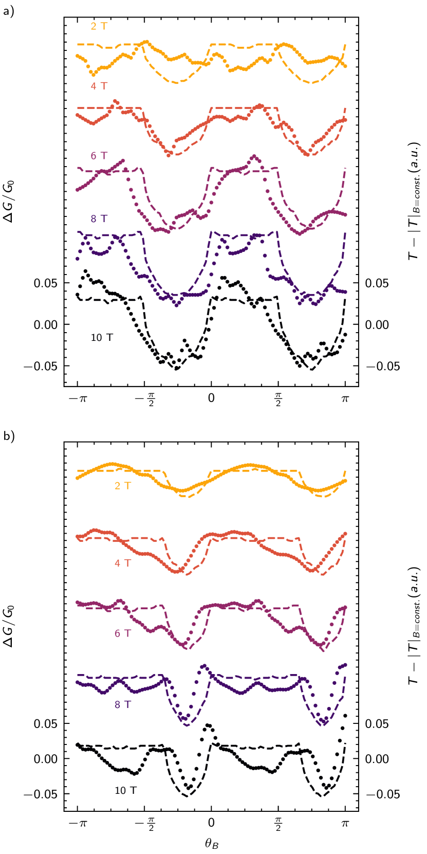
For a more detailed comparison of the angle-dependent conductance pattern between the experimental results and the simulations, we take linecuts at certain magnetic fields. Figure 3 displays linecuts of the effective conductance change in comparison to linecuts of the normalized transmission at magnetic fields ranging from 2 to , respectively, as a function of in-plane magnetic field angle. Note that the normalized transmission is rescaled and shifted to fit the scale of the conductance changes, in order to compare the angle-dependent -periodic pattern. At the linecuts above , simulation and experiment are in very good agreement. For magnetic field strengths of and less, no periodic behaviour of the effective conductance can be seen (cf. Fig. 2 c)).
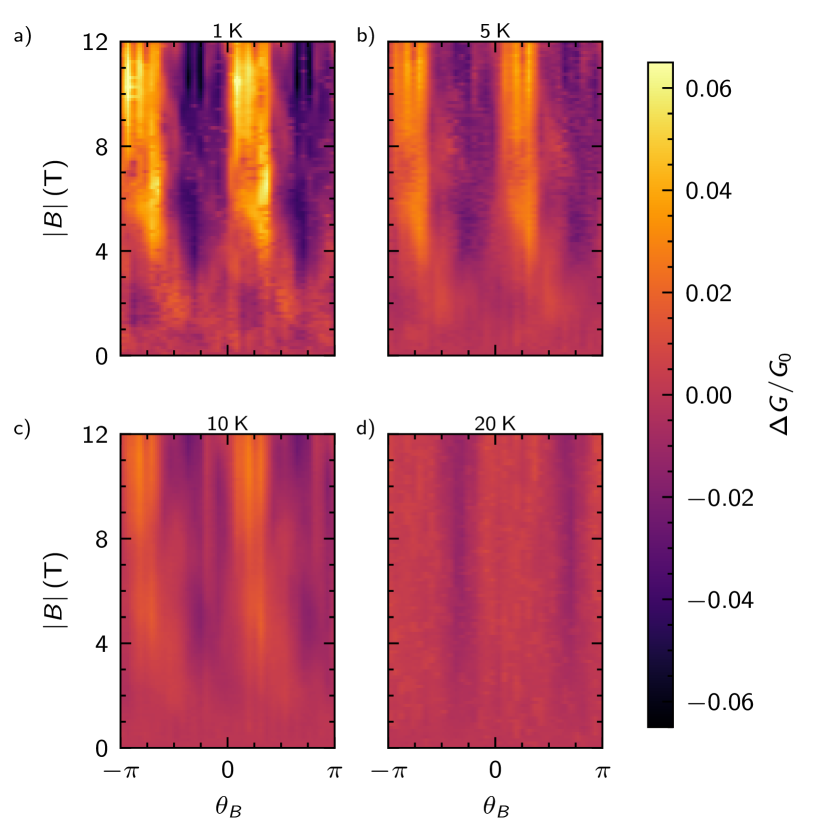
Figure 4 shows the temperature-dependent effective conductance of the kink for four different temperatures ranging from 1 to 20 K. The color scheme for all temperatures is normalized to that of the measurement. A vanishing asymmetry can be seen, with the pattern completely disappearing at temperatures above . The impact of the in-plane magnetic field on the conductance due to trapping of surface states on certain side facets of the nanoribbon is only expected to occur when the surface states are phase-coherent around the circumference of the ribbon, i.e., at sufficiently low temperatures. At elevated temperatures, e.g. at 20 K, phase coherence is lost so that the surface states on the different side facets are effectively independent and there can be no depletion of either top or bottom surface of the ribbon.
IV Conclusion
In conclusion, for 3D topological nanoribbon-based and kink structures we observed pronounced modulations in the conductance upon varying the in-plane magnetic field orientation. From the decrease of the modulation pattern with increasing temperature we deduced that the effect is based on phase-coherent carriers. In a semiclassical picture, the modulations can be explained by an orbital effect trapping electrons in the topological surface states either on the upper or lower surface of the nanoribbon legs, which affects their transmission probability across the kink. Our experimental results are in good agreement with the theoretically expected transport behavior, and consistent with the differences expected for different kink angles. The transport properties of TI nanoribbon-based kinks with an in-plane magnetic field offer interesting perspectives for the design of topological quantum circuits. The orbital effect could be exploited to drive a kink-shaped TI Josephson junction into the topological regime with Majorana states, while also offering a tuning knob for the Josephson energy through modulation of the surface-state transparency.
V Acknowledgments
We thank Herbert Kertz for technical assistance, and Florian Lentz and Stefan Trellenkamp for electron beam lithography. This work was partly funded by the Deutsche Forschungsgemeinschaft (DFG, German Research Foundation) under Germany’s Excellence Strategy - Cluster of Excellence Matter and Light for Quantum Computing (ML4Q) EXC 2004/1 – 390534769. K.M. acknowledges the financial support by the Bavarian Ministry of Economic Affairs, Regional Development and Energy within Bavaria’s High-Tech Agenda Project ”Bausteine für das Quantencomputing auf Basis topologischer Materialien mit experimentellen und theoretischen Ansätzen” (grant no. 07 02/686 58/1/21 1/22 2/23).
References
- Hasan and Kane [2010] M. Z. Hasan and C. L. Kane, Rev. Mod. Phys. 82, 3045 (2010).
- Qi and Zhang [2011] X.-L. Qi and S.-C. Zhang, Rev. Mod. Phys. 83, 1057 (2011).
- Nayak et al. [2008] C. Nayak, S. H. Simon, A. Stern, M. Freedman, and S. D. Sarma, Rev. Mod. Phys. 80, 1083 (2008).
- Alicea [2012] J. Alicea, Rep. Prog. Phys. 75, 076501 (2012).
- Hyart et al. [2013] T. Hyart, B. van Heck, I. C. Fulga, M. Burrello, A. R. Akhmerov, and C. W. J. Beenakker, Phys. Rev. B 88, 035121 (2013).
- Sarma et al. [2015] S. D. Sarma, M. Freedman, and C. Nayak, npj Quantum Inf. 1, 1 (2015).
- Aasen et al. [2016] D. Aasen, M. Hell, R. V. Mishmash, A. Higginbotham, J. Danon, M. Leijnse, T. S. Jespersen, J. A. Folk, C. M. Marcus, K. Flensberg, and J. Alicea, Phys. Rev. X 6, 031016 (2016).
- Cook and Franz [2011] A. Cook and M. Franz, Phys. Rev. B 84, 201105 (2011).
- Cook et al. [2012] A. M. Cook, M. M. Vazifeh, and M. Franz, Phys. Rev. B 86, 155431 (2012).
- Manousakis et al. [2017] J. Manousakis, A. Altland, D. Bagrets, R. Egger, and Y. Ando, Phys. Rev. B 95, 165424 (2017).
- de Juan et al. [2019] F. de Juan, J. H. Bardarson, and R. Ilan, SciPost Phys. 6, 060 (2019).
- Legg et al. [2021] H. F. Legg, D. Loss, and J. Klinovaja, Phys. Rev. B 104, 165405 (2021).
- Legg et al. [2022] H. F. Legg, D. Loss, and J. Klinovaja, Phys. Rev. B 105, 155413 (2022).
- Heffels et al. [2023] D. Heffels, D. Burke, M. R. Connolly, P. Schüffelgen, D. Grützmacher, and K. Moors, Nanomaterials 13, 723 (2023).
- Peng et al. [2010] H. Peng, K. Lai, D. Kong, S. Meister, Y. Chen, X.-L. Qi, S.-C. Zhang, Z.-X. Shen, and Y. Cui, Nat. Mater. 9, 225 (2010).
- Xiu et al. [2011] F. Xiu, L. H. Wang, L. Cheng, L.-T. Chang, M. Lang, G. Huang, X. Kou, Y. Zhou, X. Jiang, Z. Chen, J. Zou, A. Shailos, and K. L. Wang, Nat. Nanotechnol. 6, 216 (2011).
- Dufouleur et al. [2013] J. Dufouleur, L. Veyrat, A. Teichgräber, S. Neuhaus, C. Nowka, S. Hampel, J. Cayssol, J. Schumann, B. Eichler, O. G. Schmidt, B. Büchner, and R. Giraud, Phys. Rev. Lett. 110, 186806 (2013).
- Arango et al. [2016] Y. C. Arango, L. Huang, C. Chen, J. Avila, M. C. Asensio, D. Grützmacher, H. Lüth, J. G. Lu, and T. Schäpers, Sci. Rep. 6, 29493 (2016).
- Jauregui et al. [2015] L. A. Jauregui, M. T. Pettes, L. P. Rokhinson, L. Shi, and Y. P. Chen, Sci. Rep. 5, 8452 (2015).
- Kölzer et al. [2020] J. Kölzer, D. Rosenbach, C. Weyrich, T. W. Schmitt, M. Schleenvoigt, A. R. Jalil, P. Schüffelgen, G. Mussler, V. E. Sacksteder IV, D. Grützmacher, H. Lüth, and T. Schäpers, Nanotechnology 31, 325001 (2020).
- Rosenbach et al. [2020] D. Rosenbach, N. Oellers, A. R. Jalil, M. Mikulics, J. Kölzer, E. Zimmermann, G. Mussler, S. Bunte, D. Grützmacher, H. Lüth, and T. Schäpers, Adv. Electron. Mater. 6, 2000205 (2020).
- Kim et al. [2020] H.-S. Kim, T.-H. Hwang, N.-H. Kim, Y. Hou, D. Yu, H.-S. Sim, and Y.-J. Doh, ACS Nano 14, 14118 (2020).
- Scanlon et al. [2012] D. O. Scanlon, P. D. C. King, R. P. Singh, A. de la Torre, S. M. Walker, G. Balakrishnan, F. Baumberger, and C. R. A. Catlow, Adv. Mater. 24, 2154 (2012).
- Lošt’ák et al. [1989] P. Lošt’ák, Z. Starỳ, J. Horák, and J. Pancíř, Phys. Status Solidi A 115, 87 (1989).
- Kölzer et al. [2021] J. Kölzer, K. Moors, A. R. Jalil, E. Zimmermann, D. Rosenbach, L. Kibkalo, P. Schüffelgen, G. Mussler, D. Grützmacher, T. L. Schmidt, et al., Commun. Mater. 2, 1 (2021).
- Moors et al. [2018] K. Moors, P. Schüffelgen, D. Rosenbach, T. Schmitt, T. Schäpers, and T. L. Schmidt, Phys. Rev. B 97, 245429 (2018).
- Kim et al. [2011] Y. S. Kim, M. Brahlek, N. Bansal, E. Edrey, G. A. Kapilevich, K. Iida, M. Tanimura, Y. Horibe, S.-W. Cheong, and S. Oh, Phys. Rev. B 84, 073109 (2011).
- Ren et al. [2011] Z. Ren, A. A. Taskin, S. Sasaki, K. Segawa, and Y. Ando, Phys. Rev. B 84, 165311 (2011).
- Arakane et al. [2012] T. Arakane, T.and Sato, S. Souma, K. Kosaka, K. Nakayama, M. Komatsu, T. Takahashi, Z. Ren, K. Segawa, and Y. Ando, Nature Communications 3, 636 (2012).
- Kampmeier et al. [2016] J. Kampmeier, C. Weyrich, M. Lanius, M. Schall, E. Neumann, G. Mussler, T. Schäpers, and D. Grützmacher, J. Cryst. Growth 443, 38 (2016).
- Jalil et al. [2023] A. R. Jalil, P. Schüffelgen, H. Valencia, M. Schleenvoigt, C. Ringkamp, G. Mussler, M. Luysberg, J. Mayer, and D. Grützmacher, Nanomaterials 13, 354 (2023).
- Zimmermann et al. [2023] E. Zimmermann, J. Kölzer, M. Schleenvoigt, D. Rosenbach, G. Mussler, P. Schüffelgen, T. Heider, L. Plucinski, J. Schubert, H. Lüth, D. Grützmacher, and T. Schäpers, Semicond. Sci. Tech. 38, 035010 (2023).
- Hikami et al. [1980] S. Hikami, A. I. Larkin, and Y. Nagaoka, Prog. Theor. Phys. 63, 707 (1980).
- Lee et al. [1987] P. A. Lee, A. D. Stone, and H. Fukuyama, Phys. Rev. B 35, 1039 (1987).
Supplemental Material for
In-plane magnetic field-driven conductance modulations in topological insulator kinks
To explain the origin of the angle-modulated conductance pattern, we consider the impact of the orbital effect on the topological surface states in a semiclassical picture, analogous to the treatment of the steering effect in a topological insulator-based T-junction in Ref. [1]. On the top and bottom facets of the ribbon, the Lorentz force points perpendicular to the surface and can be neglected for surface-state motion that is bound to the surface of the ribbon. On the side facets (assumed to be perpendicular to the plane here), however, the Lorentz force induces a circular motion of the charge carriers with gyroradius , with the Fermi energy, the magnetic field component perpendicular to the side facet, and the Dirac velocity of the topological surface states (). Depending on the transverse velocity of the surface state, the state will be able to traverse the side facet from bottom to top (or vice versa) or not. We can quantify this condition in terms of the transverse extent of the orbital motion , given by:
| (S1) |
with () the velocity component along (perpendicular to) the ribbon, the relative angle between the ribbon and the in-plane magnetic field, the generalized quantum number for the transverse wave number of the topological surface state, , including contributions of the transverse orbital motion, the nontrivial Berry phase , and the magnetic flux enclosed by the perimeter of the ribbon cross section in units of the flux quantum . When the transverse extent is smaller than the height of the ribbon, the state cannot traverse the side facet (see Fig. S1). For surface states that wrap phase-coherently around the perimeter of the ribbon cross section, it follows that the top or bottom surface effectively gets depleted (or, equivalently, trapped on the opposite surface). When the surface states on the two legs of the kink are trapped on opposite facets of the ribbon, the transmission of these states across the kink is suppressed.
In the Supplementary Material of Ref. [2], it was also shown that the steering effect is only expected for states that are located on the surface, and that the robustness of the effect against disorder is greatly enhanced by spin-momentum locking, which suppresses scattering processes with a significant change in momentum. The observed magnetoconductance pattern is therefore not likely to originate from trivial bulk states or trivial surface states without spin-momentum locking. Hence, in-plane magnetic field dependence of the conductance across TI nanostructures (e.g., kinks or multiterminal junctions) provides a robust transport signature of topological surface states.
References
- Moors et al. [2018] K. Moors, P. Schüffelgen, D. Rosenbach, T. Schmitt, T. Schäpers, and T. L. Schmidt, Phys. Rev. B 97, 245429 (2018).
- Kölzer et al. [2021] J. Kölzer, K. Moors, A. R. Jalil, E. Zimmermann, D. Rosenbach, L. Kibkalo, P. Schüffelgen, G. Mussler, D. Grützmacher, T. L. Schmidt, et al., Commun. Mater. 2, 1 (2021).