[1]H. Rueda
Timing performances of NectarCAM, a Medium Sized Telescope Camera for the Cherenkov Telescope Array
Abstract
NectarCAM is a Cherenkov camera that will be installed on Medium-Sized Telescopes of the northern array of the Cherenkov Telescope Array Observatory (CTAO). It is composed of 265 modules, each of which includes 7 photo-multiplier tubes, a Front-End Board and a camera trigger system for data collection. The first NectarCAM unit is currently being integrated at CEA Paris-Saclay in France. Once installed at the CTAO’s northern site, the NectarCAM’s timing abilities will be crucial for reducing noise in images, improving image cleaning, and distinguishing between gamma-ray photons and cosmic-ray background. Additionally, it will enable coincidence identification with neighboring telescopes for stereoscopic observations. The timing system of NectarCAM has been tested in a dark room with various light sources. The results of the tests, including timing precision and accuracy of the trigger arrival relative to a laser source, and the timing of individual and multiple pixel signals, will be presented.
1 Introduction
The Cherenkov Telescope Array Observatory (CTAO) [1, 2] is a next-generation ground-based observatory designed to detect very high-energy gamma rays from celestial sources. The CTAO will consist of an array of 68 imaging atmospheric Cherenkov telescopes (IACTs) located at two sites in the northern and southern hemispheres. These ground telescopes detect the faint flashes of Cherenkov radiation produced when very high energy (VHE) gamma-rays111from a few tens of GeV to above 100 TeV [1] from space interact with the Earth’s atmosphere. The CTAO is designed to improve the capabilities of existing gamma-ray observatories by providing a more extensive collection area and broader energy coverage [3]. The array will have three size classes of telescopes: large-sized telescopes (LSTs) for low-energy gamma rays, medium-sized telescopes (MSTs) for intermediate energies, and small-sized telescopes (SSTs) for the highest energies, allowing a wide range of gamma-ray energies, from 20 GeV to 300 TeV. NectarCAM [4] is a type of camera developed for the CTAO. It is specifically designed to be used with the medium-sized telescopes (MSTs) of the CTA, which are optimized for detecting gamma rays in the medium energy range.
The NectarCAM camera utilizes a modular design consisting of a focal plane module (FPM) and a front-end board (FEB). The FPM [5] comprises seven Hamamatsu photomultiplier tubes (PMTs) with Winston cone light concentrators [6]. These PMTs detect the Cherenkov light and convert it into an electric signal, which is then preamplified and split into low and high gain channels and a trigger channel in the FEB. The NECTAr chip [7] plays a crucial role in sampling and digitizing the signal at a rate of 1 GHz, utilizing a 12-bit analog-to-digital converter. This chip acts as a circular buffer, holding the data until a camera trigger event occurs.
The triggering mechanism of the NectarCAM camera involves detecting a significant amount of light within a compact region of the focal plane, typically spanning around or three pixels, within a short time frame [8]. Neighboring modules are triggered first (level 0 trigger or L0), followed by the camera itself (level 1 or L1, and level 2 or L2) through the combination of digitized signals at the digital trigger (DT) system. The L0 trigger is processed in each FEB using application-specific integrated circuits (ASICs), and the resulting digital signal is sent to a Field-Programmable Gate Array (FPGA) on the respective module’s digital trigger backplane (DTB). The L1 trigger signal is then formed by processing the L0 signals from the module and its six neighboring modules, creating a 37-pixel region. This process ensures trigger homogeneity throughout the camera.
In evaluating the NectarCAM qualification model, particular focus was placed on timing accuracy and systematic uncertainties [9]. The aim was to characterize the camera’s performance by accurately timestamping triggers and estimating the arrival time of light in each pixel. These metrics are crucial in reducing noise in shower images, improving imaging cleaning, and enhancing the differentiation between Cherenkov photons and background signals.
2 Test setup
The first NectarCAM camera has been integrated at the CEA Paris-Saclay test facility. The facility includes a thermalized dark room with camera services and calibration light sources, connected to a control room housing the data acquisition (DAQ) [10], storage, and control systems. The camera comprises readout electronics with 1855 pixels distributed in 265 modules and is connected to a dedicated camera server via 10 Gb/s optical links. A separate camera slow control server handles all camera devices from the control room.
Three light sources, at a distance of 12 m from the center of NectarCAM, were used for camera evaluation: a flat field calibration light source (FFCLS) with 13 light-emitting diodes (LED); a continuous night sky background (NSB); and a laser source. The FFCLS emits pulsed light at 390 nm wavelength, reproducing the maximum of the received UV Cherenkov spectrum. The 519 nm LED NSB source reproduces the median photoelectron rate of the typical night sky spectrum. The laser source provides uniform illumination at 373 nm wavelength and is used for precise timing measurements.
The time of maximum (TOM) represents the reconstructed arrival time of a signal from a photomultiplier tube (PMT). The PMT signal is sampled every nanosecond within a 60-nanosecond window. By analyzing the waveform after subtracting the pedestal, the TOM is determined by finding the position of the pulse’s maximum. Precise measurements of the camera’s timing performance are conducted using a laser connected to a Timing and Clock-Stamping (TiCkS) board which timestamps the laser’s output pulse, enabling accurate evaluation of the camera’s timing capabilities by comparison with the camera’s trigger timestamp produced by another TiCkS board in the Unified Clock and Time-Stamping (UCTS) module described later.
3 Single pixel timing precision
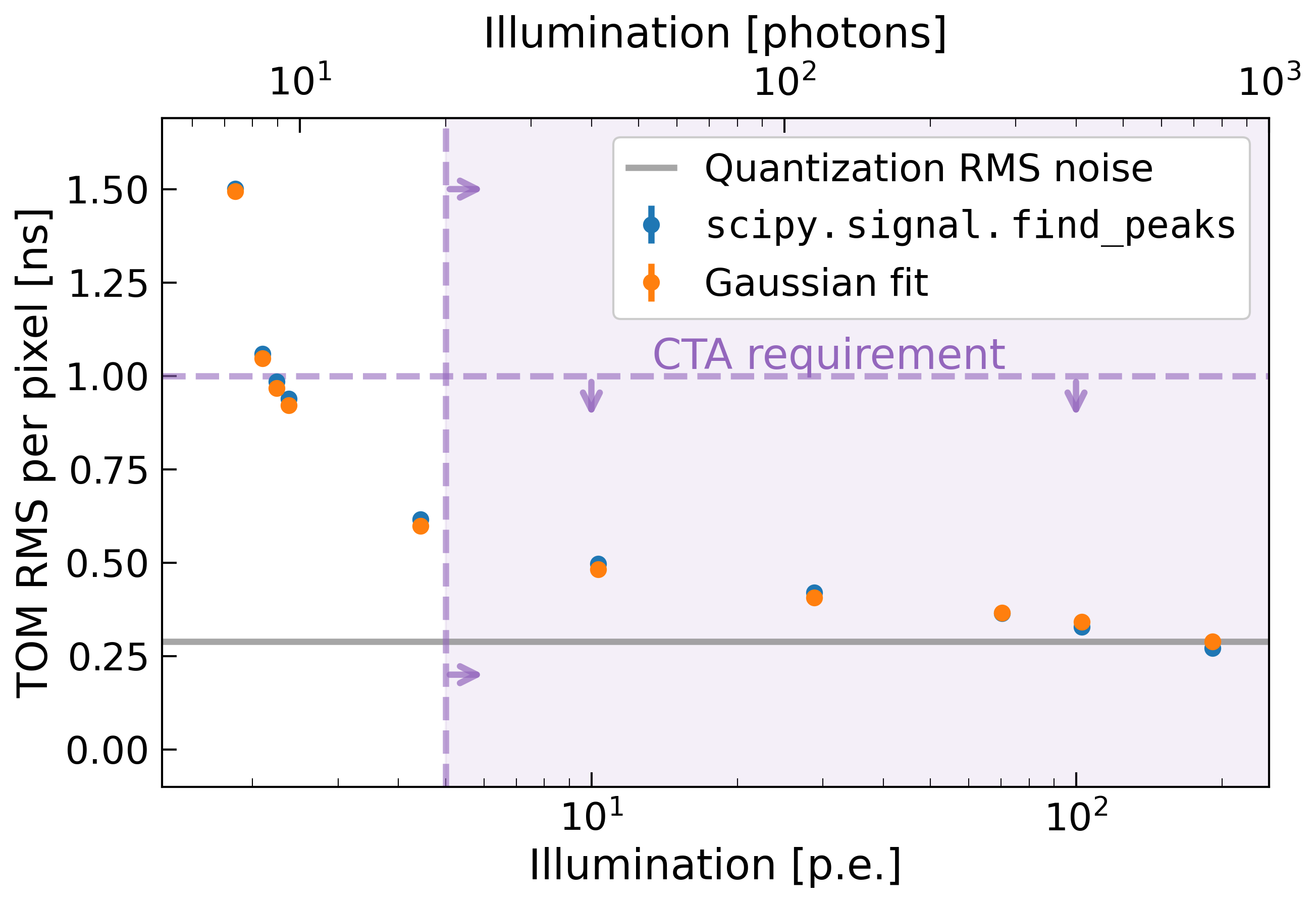
In this section, we evaluate the systematic timing uncertainty of each pixel in the NectarCAM. In order to meet the requirements of the CTAO, the NectarCAM camera needs to achieve a single pixel timing precision better than 1 ns for a light illumination above 20 photons (equivalent to 5 photoelectrons).
We conduct experiments by illuminating the camera with a laser source, generating uniform light at frequencies of 1 kHz and intensities ranging from 8.0 nW to 20 nW. The time of maximum (TOM) of each photon pulse is measured for every pixel using two methods: identifying the largest peak position and fitting a Gaussian curve to the peak. Both methods yield consistent results within 50 ps. The timing uncertainty of each pixel is determined by calculating the TOM distribution’s root mean square (RMS).
Figure 1 displays the weighted mean of the TOM RMS values for all pixels as a function of the illumination charge computed from both methods. It shows that for light intensities above approximately 10 photons, both methods achieve a time resolution of less than 1 ns. This meets the CTAO requirement, stating that the RMS uncertainty on the mean relative reconstructed arrival time in each camera pixel should not exceed 1 ns for photon amplitudes ranging from 20 to 2000 photons per pixel. This is represented by the violet area. However, at a light illumination of 800 photons, the pixel time precision reaches its limit (gray dashed line), corresponding to the quantified RMS noise of 1/ ns.
4 PMT transit time correction
Prior to estimating the camera’s overall timing precision, a relative calibration of the TOM is necessary to synchronize the 1855 pixels in the camera. Two systematic effects cause a timing offset between pixels. Timing offsets are influenced by variations in the arrival times of the Level 1 Accept (L1A) trigger signal sent back from the TIB due to FPGA jitter in the Digital Trigger Boards (DTBs) [11]. Calibrating the dispersion in L1A delay involves adjusting delays in the digital backplanes and can be performed with an ordinary data-taking run.
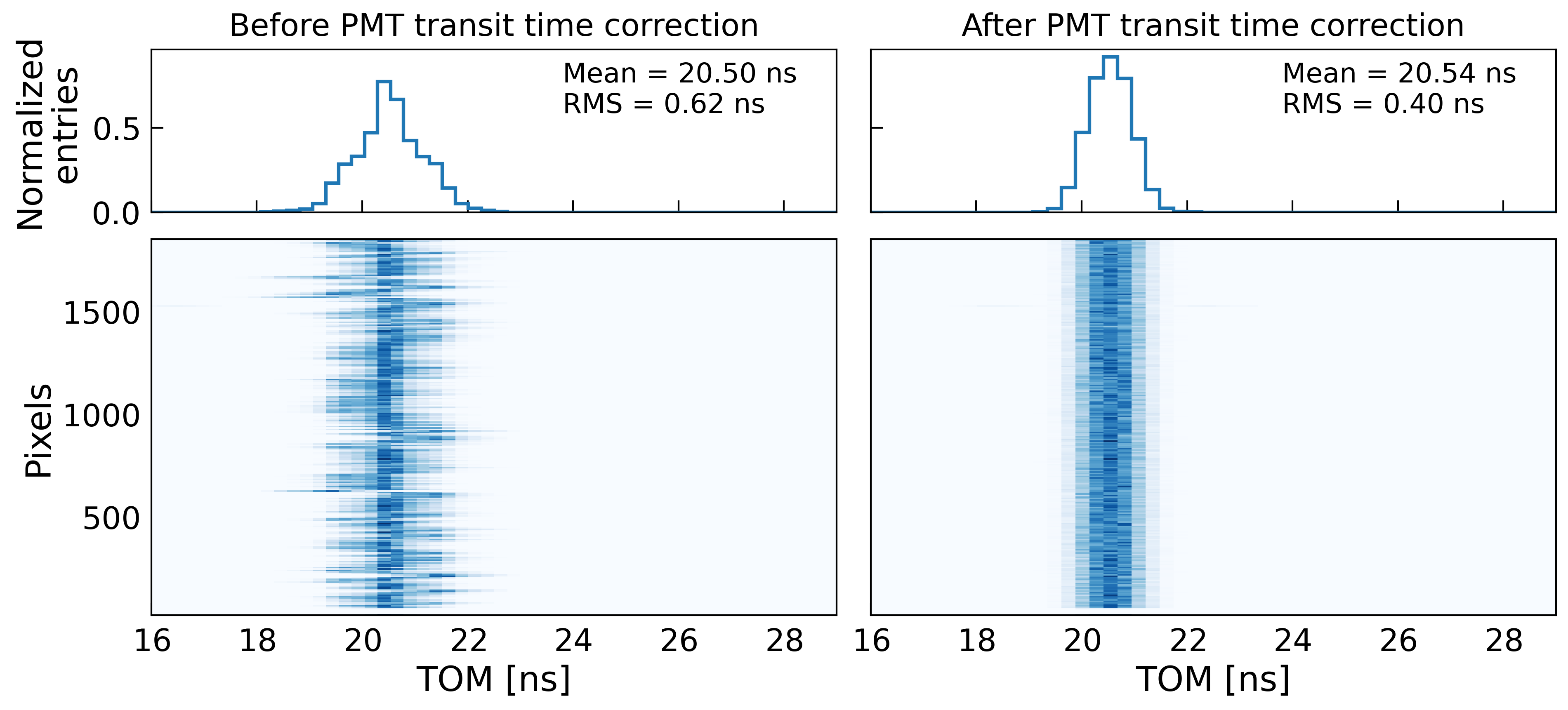
Another effect is the PMT transit time, which can only be addressed after analysis. The PMT transit time, which refers to the transfer time of the electron avalanche in the PMT [12] and depends on the high voltage applied to the dynodes, introduces delays in the camera. In order to maintain a nominal gain of 40000 across the camera’s detection plane, different voltages are selected for each pixel, resulting in varying delays that typically degrade timing performances, if not corrected for. Particularly for gamma-ray energies below 100 GeV [13], the drop in telescope performance in terms of effective area becomes noticeable.
Figure 2 left panel illustrates the impact of transit time spread between pixels. It shows that the mean time of maximum (TOM) distributions for all pixels are not aligned but exhibit a time shift. To correct this effect, all pixels were set to voltages ranging from 700 V to 1100 V and illuminated with various intensities from 13 LEDs. The dependence of each pixel’s TOM as a function of their nominal voltage was evaluated by performing a least-squares fit. Then, the PMT transit time effect was corrected by shifting the TOM values to align with the fit value at 1000 V for each pixel. The right panel of Figure 2 depicts the synchronized mean TOM distributions after the correction, where the PMT transit time RMS is significantly reduced.
5 Global pixel timing precision
The CTAO requirement for the RMS of the time of maximum difference distribution for any two simultaneously illuminated pixels is 2 ns. To evaluate the timing resolution of the camera after the PMT transit time correction, we illuminate the camera with a p.e. uniform light using the laser source.
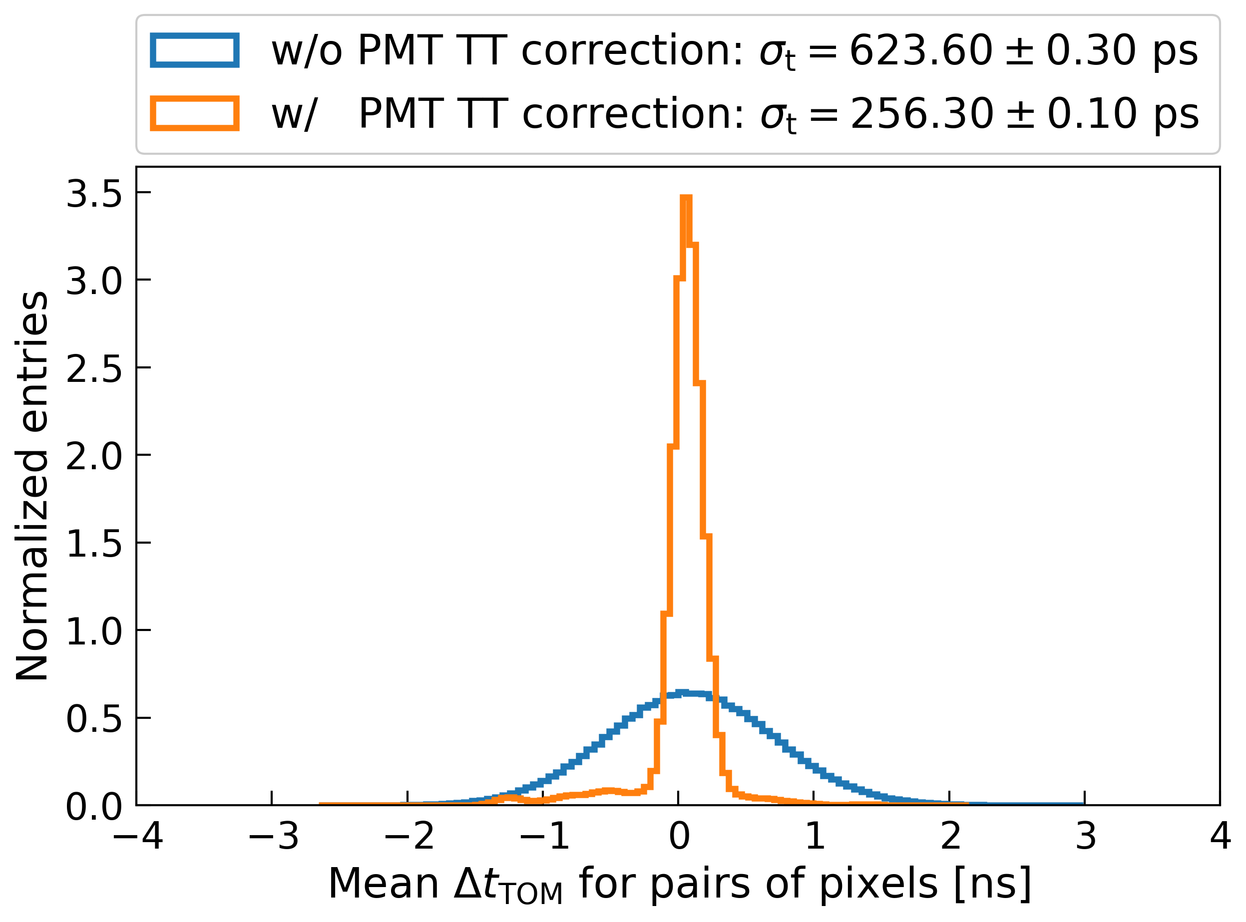
For all pixel pairs, the TOM difference () is calculated with and without PMT transit time correction. Figure 3 shows the mean distribution of for each pair of pixels, showing significant improvement after calibration. We see that the RMS of the distribution is reduced from 623.60 ps to 256.30 ps after the correction, meeting the 2 ns CTAO requirement.
6 Camera trigger timing accuracy
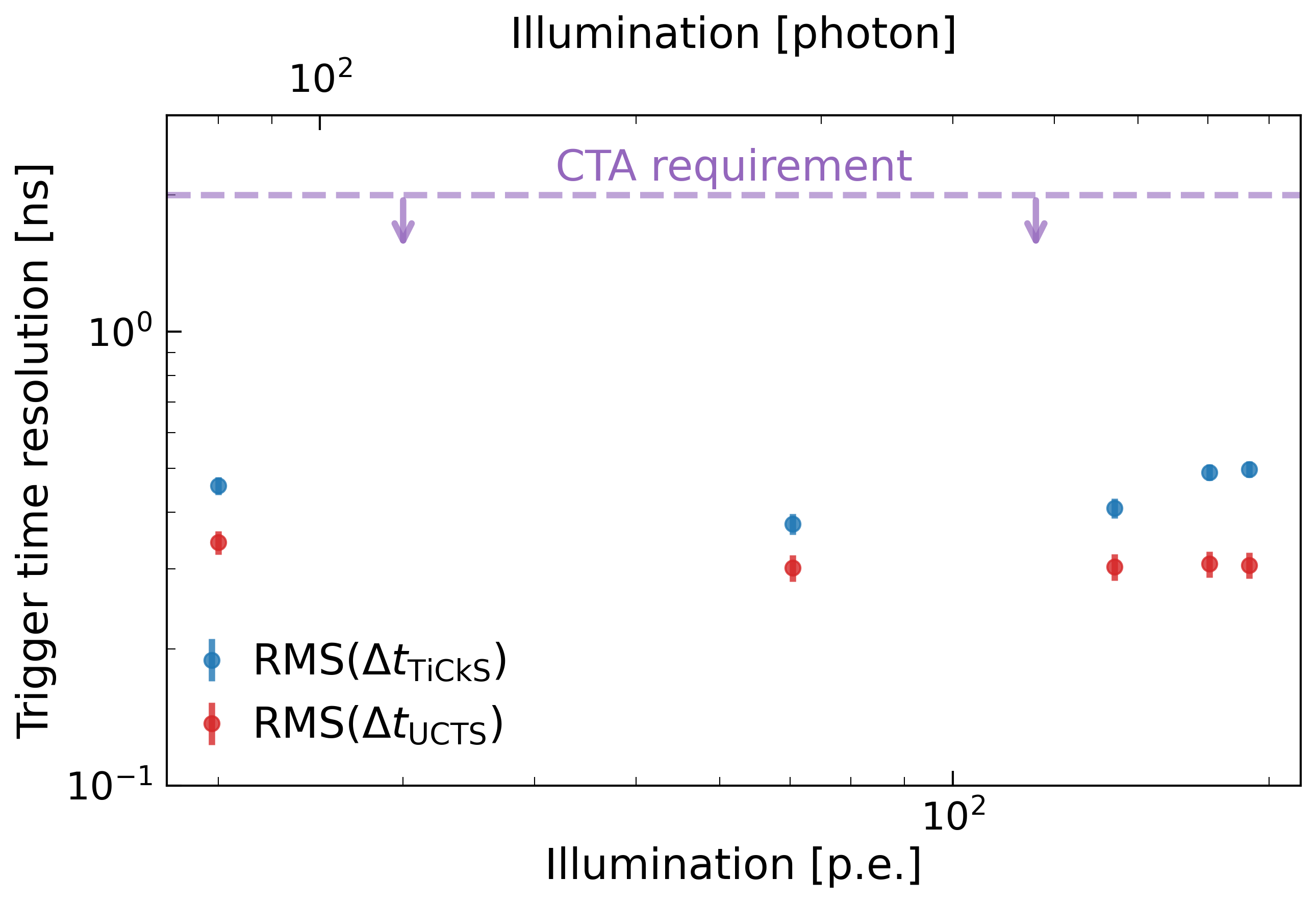
As we mentioned, the TiCkS board of the UCTS module is responsible for time-stamping the events captured by the camera. In order to ensure effective coordination and synchronization of observations across the entire CTAO array, achieving a high level of timing accuracy is crucial. We illuminate the entire camera using a laser source at 1 kHz with intensities ranging from 20 p.e. to 191 p.e. The start times of the laser flashes were recorded with an external TiCkS board. With this configuration, two different analyses are employed to quantify the RMS of the timestamp distribution.
The first method consists in comparing the laser flashes time stamp with the light arrival UCTS in the detection plane of the camera (). The second analysis evaluates the distribution of the time difference between two consecutive events, expected to be ns for a 1kHz flash. The camera’s response to photons emitted by the laser, reaching the TIB and sending us its trigger pulse, is at most 245 ns, taking into account the 12 m distance between the laser and the camera’s focal plane. The RMS values obtained for each configuration are presented in Figure 4. The trigger timing accuracy achieved with both methods is consistent and better than 0.5 ns, below the CTAO requirements.
7 Conclusion
The NectarCAM timing system has been evaluated and tested in a controlled environment, at the CEA Paris-Saclay facility. The camera has demonstrated to fullfill the CTAO timing requirements, crucial for the precise analysis of data collected. The experiments on single-pixel timing precision show that the camera achieves a time resolution of less than 1 ns for light intensities above 10 photons. The PMT transit time calibration effectively reduces the timing offsets between pixels, improving the overall timing precision of the camera. After calibration, the global pixel timing precision satisfies the CTAO requirement of 2 ns for the RMS of the TOM difference distribution between any two simultaneously illuminated pixels. Additionally, the camera trigger timing accuracy has been evaluated using a laser source, and the results demonstrate that the trigger timing is better than 0.5 ns, surpassing the CTAO requirements.
Acknowledgments
This work was conducted in the context of the CTA Consortium. We gratefully acknowledge financial support from the agencies and organizations listed here: https://www.cta-observatory.org/consortium_acknowledgments/.
References
- [1] B. Acharya et al. Astroparticle Physics 43 (2013) 3–18. Seeing the High-Energy Universe with the Cherenkov Telescope Array - The Science Explored with the CTA.
- [2] M. Actis et al. Experimental Astronomy 32 no. 3, (Nov, 2011) 193–316.
- [3] K. Bernlöhr et al. Astroparticle Physics 43 (2013) 171–188. Seeing the High-Energy Universe with the Cherenkov Telescope Array - The Science Explored with the CTA.
- [4] CTA Consortium Collaboration, J.-F. Glicenstein PoS ICRC2015 (2016) 937.
- [5] A. Tsiahina et al. Nuclear Instruments and Methods in Physics Research A 1007 (Aug., 2021) 165413.
- [6] F. Hénault et al., “Design of light concentrators for Cherenkov telescope observatories,” in Nonimaging Optics: Efficient Design for Illumination and Solar Concentration X, R. Winston and J. Gordon, eds., vol. 8834 of Society of Photo-Optical Instrumentation Engineers (SPIE) Conference Series, p. 883405. Sept., 2013.
- [7] E. Delagnes et al., “NECTAr0, a new high speed digitizer ASIC for the Cherenkov Telescope Array,” in 2011 IEEE Nuclear Science Symposium Conference Record, pp. 1457–1462. 2011.
- [8] U. Schwanke et al. Nuclear Instruments and Methods in Physics Research Section A: Accelerators, Spectrometers, Detectors and Associated Equipment 782 (2015) 92–103.
- [9] F. Bradascio et al. Nuclear Instruments and Methods in Physics Research Section A: Accelerators, Spectrometers, Detectors and Associated Equipment 1054 (2023) 168398.
- [10] D. Hoffmann et al. Journal of Physics: Conference Series 898 no. 3, (Oct, 2017) 032015.
- [11] T. Tavernier et al. PoS ICRC2019 (2020) 805.
- [12] W. R. Leo, Techniques for nuclear and particle physics experiments: a how-to approach; 2nd ed. Springer, Berlin, 1994.
- [13] L. A. Tejedor et al. IEEE Transactions on Nuclear Science 60 no. 4, (2013) 2905–2911.