Design and Performance of Parallel-channel Nanocryotrons in Magnetic Fields
Abstract
We introduce a design modification to conventional geometry of the cryogenic three-terminal switch, the nanocryotron (nTron). The conventional geometry of nTrons is modified by including parallel current-carrying channels, an approach aimed at enhancing the device’s performance in magnetic field environments. The common challenge in nTron technology is to maintain efficient operation under varying magnetic field conditions. Here we show that the adaptation of parallel channel configurations leads to an enhanced gate signal sensitivity, an increase in operational gain, and a reduction in the impact of superconducting vortices on nTron operation within magnetic fields up to 1 Tesla. Contrary to traditional designs that are constrained by their effective channel width, the parallel nanowire channels permits larger nTron cross sections, further bolstering the device’s magnetic field resilience while improving electro-thermal recovery times due to reduced local inductance. This advancement in nTron design not only augments its functionality in magnetic fields but also broadens its applicability in technological environments, offering a simple design alternative to existing nTron devices.
The superconducting nanowire cryotron (nTron) is a current-based three terminal device that is the natural evolution of the original macroscopic cryotron superconducting switch Buck (1956). Compared to the related Josephson junction-based devices, the nTron has an ultra-compact size, insensitivity to magnetic noise, and the ability to be integrated into larger superconducting and semiconductor hybrid circuits McCaughan and Berggren (2014); Tanaka et al. (2017); Zhao et al. (2017, 2018); McCaughan et al. (2019); Zheng et al. (2020). In addition, nTron fabrication and design can be tuned to fit a range of applications such as signal amplification and digital logic Krylov and Friedman (2019); Huang et al. (2023). This makes the nTron a desirable candidate for on chip integration with superconducting nanowire detectors. As there has been a recent uptick of demand of superconducting nanowire detectors outside of the field of nanophotonics Polakovic et al. (2020); Khalek et al. (2022), pushing the limits of timing and gain of the nTron devices, especially in high-field environments, is becoming a interesting topic to explore. Here we report on results of such investigation. We additionally report on effects of changing the conventional geometry of the nTron by including additional parallel channels to the device current-carrying channel, effectively mimicking the design of superconducting nanowire avalanche detectors Marsili et al. (2011) in efforts to increase the device speed and gain.
The performance of the nTron device depends primarily on two specifications: the width of the narrow choke at the input gate terminal and the width of the larger bias channel. The ratio between these two dimensions determines the cross-sectional area of the 2D wire and, consequently, the local critical current density Il’in et al. (2005). The primary function of an nTron is to bias the channel near . When a small input signal travels down the gate terminal and into the geometrically constricted choke, it generates a Joule-heated hot spot, increasing the channel’s resistivity and resulting in an overall signal amplification. After the input signal switches off, the total current returns below , and the hot spot diffuses outward across the channel. The choke area then reverts back to the superconducting state as it is cooled by the surrounding cold bath.
We introduce a modification to the conventional nTron by incorporating nano-patterned gaps, which effectively reduce the width of the biasing channel from the standpoint of switching operation. This transformation converts the wide-channel nTron into a smaller comparable device with lower inductance, while preserving the larger total current carrying capacity. The reduced channel inductance leads to improved device recovery time compared to the conventional nTron Kerman et al. (2009, 2006); Toomey et al. (2018); Annunziata et al. (2010). Furthermore, this reduction in effective channel width facilitates the fabrication of larger nTron cross sections compared to the traditional choke and bias design, typically ranging from tens to hundreds of nanometers, albeit the larger designs may be limited by the speed of the electro-thermal feedback of the deviceMcCaughan and Berggren (2014).
We explore two different aspect ratios and compare their DC and recovery characteristics in the presence of magnetic fields. We also study effects of patterning the bias channel into parallel nanowires, and provide conventional nTrons of similar aspect ratios for comparison.
Each nTron device was patterned from a 12 nm thick NbN film with a superconducting transition temperature = 7.6 K, deposited using ion beam assisted sputtering on a silicon substrate with a 10 nm silicon nitride underlayer Polakovic et al. (2018). These nTrons feature a gate input port that narrows into a choke constriction and connects perpendicularly to the primary biasing channel with source and drain ports. The channel near the choke is optimally tapered to maximize current density for improved hot spot sensitivity and reduced current crowding Clem and Berggren (2011); Inoue et al. (2019). We compare two parallel-channel devices with different aspect ratios to a conventional nTron design.
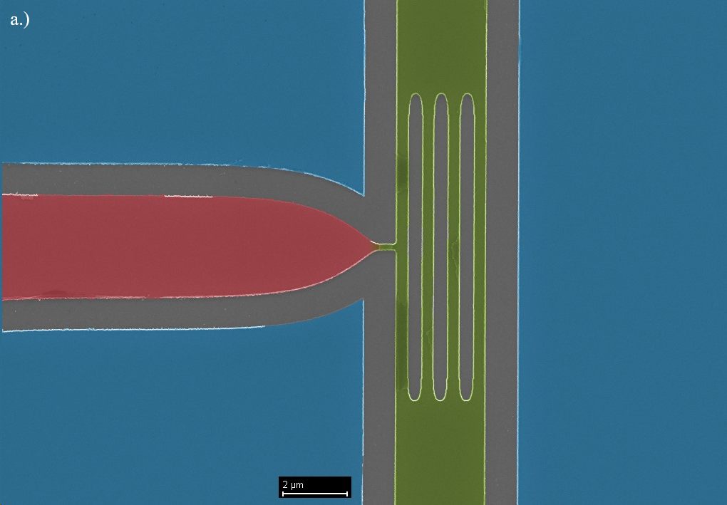
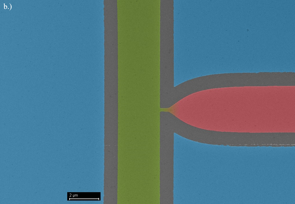
The parallel-channel nTron geometry includes three gaps within the channel of each device, with widths of 100 nm and 400 nm, and lengths 2.4 m and 9.6 m, respectively. The gaps divide the channel into four parallel wires with smaller cross sectional area near the input gate, effectively reducing the local inductance compared to an nTron with single narrow channel, from to because the four narrow channels act as inductors connected in parallel. The choke width is fixed at 200 nm for both designs, while the effective bias channel width is reduced to 400 nm (from 700 nm) and 1.6 m (from 2.8 m), creating a relative 1:2 and 1:8 aspect ratio between the narrow choke and bias channel widths. In contrast, the conventional nTrons have choke widths of 200 nm and absolute channel widths of 700 nm and 2.8 m, respectively. This compares to the size of the nTrons if the gaps were not present within the channel. Fig. 1 displays scanning electron microscope (SEM) images of both 1:8 parallel-channel and conventional nTron geometries (see supplemental material for 1:2). Table 1 summarizes the design specifications for both aspect ratios.
| nTron | Choke (nm) | Gap (nm) | Eff. Channel (m) |
|---|---|---|---|
| 1:2 (Gapped) | 200 | 100 | 0.4 |
| 1:2 (Conv.) | 200 | - | 0.7 |
| 1:8 (Gapped) | 200 | 400 | 1.6 |
| 1:8 (Conv.) | 200 | - | 2.8 |
We conducted DC characterizations on each nTron device at 1.4 K within an American Magnetics cryostat, which included a superconducting triple-axis vector magnet. We connected the device to an RF chip using aluminum wire bonds and 50 transmission cables in series with an RF/DC bias tee. To minimize heat dissipation across the channel during switching events, each nTron channel’s source and drain ports were connected in parallel to a 50 shunt Brenner et al. (2012); Toomey et al. (2018).
DC current is initially applied across the channel to characterize the critical switching current of the channel, , indicated by a sharp voltage jump. Once we determined , we bias the channel current within the range of 0.80-1.05 , applying DC current to the nTron gate to identify the critical gate switching current that initiates the weak link. We then constructed DC switching characteristic diagrams correlating for weak link generation with the chosen fixed . This process was repeated at various magnetic fields applied perpendicular to the device surface.
The switching characteristics and output performance of nTron devices depend primarily on the cross-sectional area design of the gate and channel, as well as material properties. In this study, we investigate the impact of magnetic fields on nTron device performance with the parallel-channel modification. By applying DC current to the main nTron channel (without gate input), we observed a sharp voltage rise after the scanning current surpassed the critical switching current . The introduction of a magnetic field produces Abrikosov vortices, shifting the film into a mixed superconducting state. The magnetic field produces a linear increase in residual voltage across the channel resulting from flux flow derived of the Lorentz force interaction of vortices with the biasing current. The field shifts and reduces the overall amplitude of the voltage jump during the switching transition, since before the jump, there exists some finite voltage provided by the vortex dissipation. As the channel bias approaches , intermittent voltage oscillations cycle out of the mixed superconducting state. This phenomenon is particularly pronounced in the larger 1:8 ratio devices, especially the conventional nTron. Additionally, this effect is accentuated with larger due to increased vortex number. Detailed channel and gate scans are provided in the supplemental material.
These intermittent voltage pulses result from vortex crossings in the main nanowire channel of the nTron, either directly or through preexisting hot spots generated by thermal fluctuations in the metastable state induced by higher bias currents Bulaevskii et al. (2011). Vortex-antivortex pair breaking is unlikely due to the low temperature operation at T = 1.4 K and the higher energy barrier required compared to a single vortex crossing Kitaygorsky et al. (2007). This phenomenon is especially prominent in larger aspect ratio devices, where the larger cross-section leads to a higher threshold and, consequently, higher operation bias, even without an applied magnetic field McCaughan and Berggren (2014).
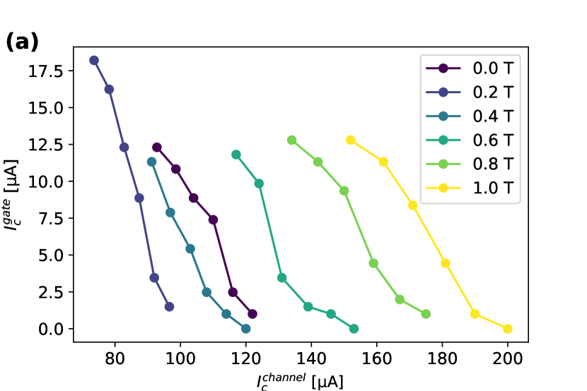
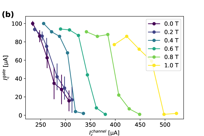
Fig. 2 shows the critical current switching relationship between the channel bias and input gate signal for both the 1:2 and 1:8 parallel-channel nTrons. Notably, the 1:2 parallel-channel nTron exhibits distinct behavior at different magnetic field strengths, characterized as "low fields" (0-0.4 T) and "high fields" (0.6-1.0 T), respectively. This suggests two regimes: one dominated by current and the other by vortices. In the low-field regime, where vortex population is smaller and flux motion weaker, the weak link transition is less sensitive to a stronger input pulse. However, as the magnetic field strength increases, the vortex interaction becomes strongly coupled to the biasing current, leading to a downshift in the critical current and increased sensitivity to the gate input signal.
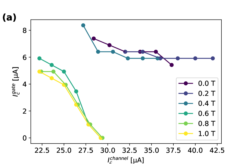
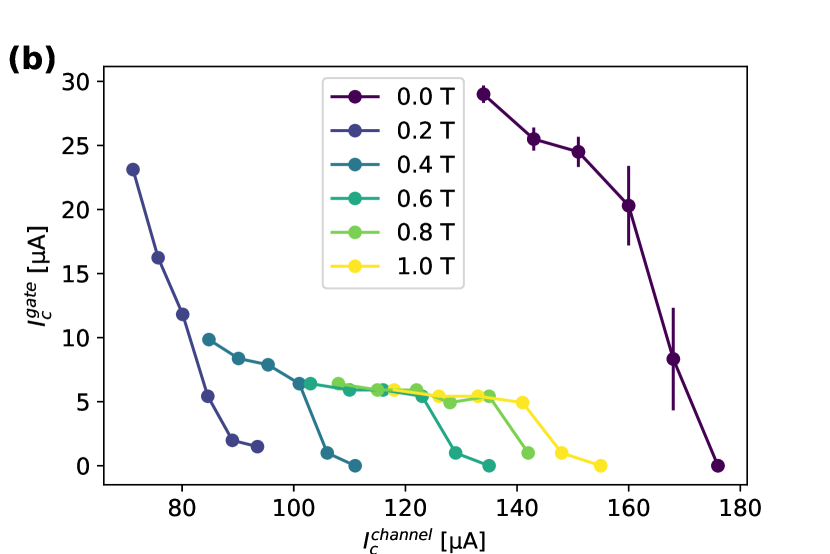
As the nTron’s aspect ratio increases, the regime shift becomes less pronounced. In Fig. 2, the 1:8 nTron displays a distinct shift in gate signal sensitivity when a magnetic field is applied, causing to decrease and gate sensitivity to plateau around 5 µA. Due to its larger primary channel, the 1:8 device exhibits stochastic switching events within a window of values. This behavior is also observed in the 1:8 conventional device, even with a small 0.2 T applied field (see Fig. 3). The more prominent switching observed in the conventional nTron is attributed to its larger channel cross-sectional area. The nano-patterned gaps, however, lower the local maximum vortex count, foster pinning, and lessen the probabilistic switching, as evident in the 1:8 design Colauto, Motta, and Ortiz (2021); Wang et al. (2013).
It is noteworthy to observe the increase in for the larger 1:2 conventional device with a wider channel compared to its parallel-channel twin device. This observation is also consistent for both 1:8 nTron designs. Previously, we described how the application of leads to a linear increase in voltage with scanning current across the channel. With increasing , the voltage jump, signaling the nTron transitioning from a mixed state to fully normal state, diminishes in amplitude and appears at higher (see Fig. S1-2 supplemental material). We focus at this distinct voltage jump which indicates a complete transition as the hotspot fully encloses the channel, opposed to the low-bias regimes where the residual voltage signal gradually increases from the zero level.
From these observations, it is inferred that the escalating field strength intensifies flux flow jamming, leading to an increased channel switching current Karapetrov et al. (2012). This escalation results in a residual voltage increase, attributable to flux flow induced by the biasing current. As the field strength increases, higher vortex density enhances the depinning force, which in turn affects the vortex mobility, leading to jamming and altered dynamics. This relationship lays the foundation for the observed voltage behavior. Initially, the voltage remains at zero. With the application of a field and the resultant screen current, a linear increase in voltage is witnessed due to flux flow. However, the sharp voltage jump marking shifts to higher values with each increase in field strength, and the amplitude of this "jump" concurrently diminishes. This behavior is ascribed to the intricate interplay between the driving current and the distorted vortex lattice. At heightened field strengths, the entire vortex lattice, now denser and more constricted, moves under the influence of the driving bias, leading to a reduced voltage gain at and altered vortex dynamics Reichhardt and Reichhardt (2010).
After determining the DC characteristics of the nTron, we measured and compared its recovery speed using two separate gate pulse techniques. Nanoseconds wide pulses were delivered to the gate via a pulse generator at variable attenuation, as the input pulse power controls the hotspot size and temperature Zheng et al. (2019). The first technique involved a double short pulse train, consisting of two brief pulses. The timing of these pulses was adjusted so that the second pulse was delivered at approximately 50% decay of the voltage signal from the first pulse. The second technique measured the step response from a long square pulse. The pulse length was 50 ns to minimize reflections and other transient effects. We measured the voltage signal across the channel using a Lecroy oscilloscope connected by a bias tee. The time constant was extracted from the decaying tail of the voltage signal using an exponential decay fitting function: . This procedure was repeated at different amplitudes of up to 1.0 T.
Pulse and attenuation parameters were scanned to optimize the signal-to-noise ratio while minimizing any latching caused by reflections or over stimulation of the gate Zheng et al. (2019). The primary pulse parameters included applied gate voltage, pulse attenuation, pulse duration, and pulse spacing (for the double pulse only). Detailed pulse parameters for each nTron device in its respective field environment are provided in the supplemental material. The maximum voltage output varied in different bias and field environments from the trade off of input power to recovery time. In addition, some latching and reflection was unavoidable at fixed attenuation in order to have distinguishable signal-to-noise ratio, making the measurement of the actual recovery difficult in some cases.
Fig. 4 shows the relaxation times for biases at 0.80-1.0 of the 1:2 and 1:8 nTrons with parallel channels. The longer relaxation times at low bias and zero field are likely due to direct cooling from the substrate, rather than the faster dynamics of the superconductor in high-field environments Kerman et al. (2009).
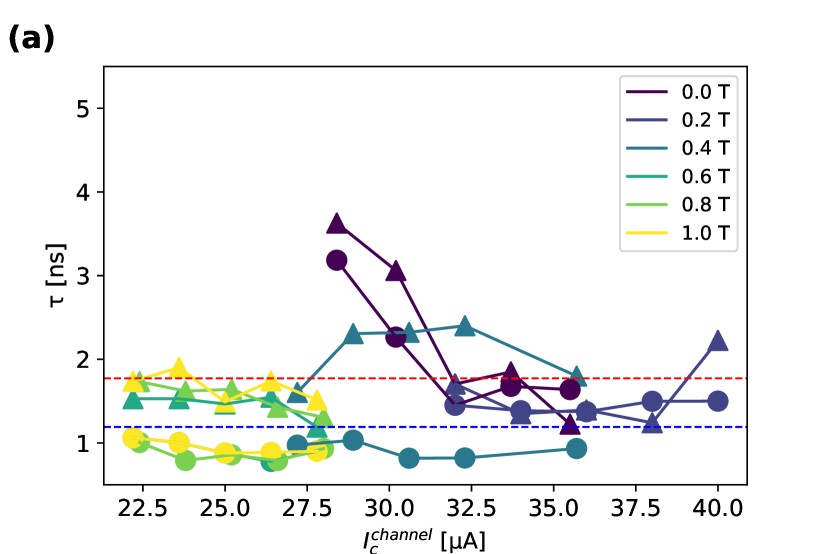
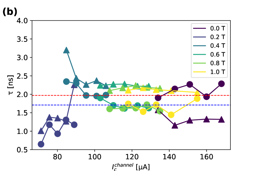
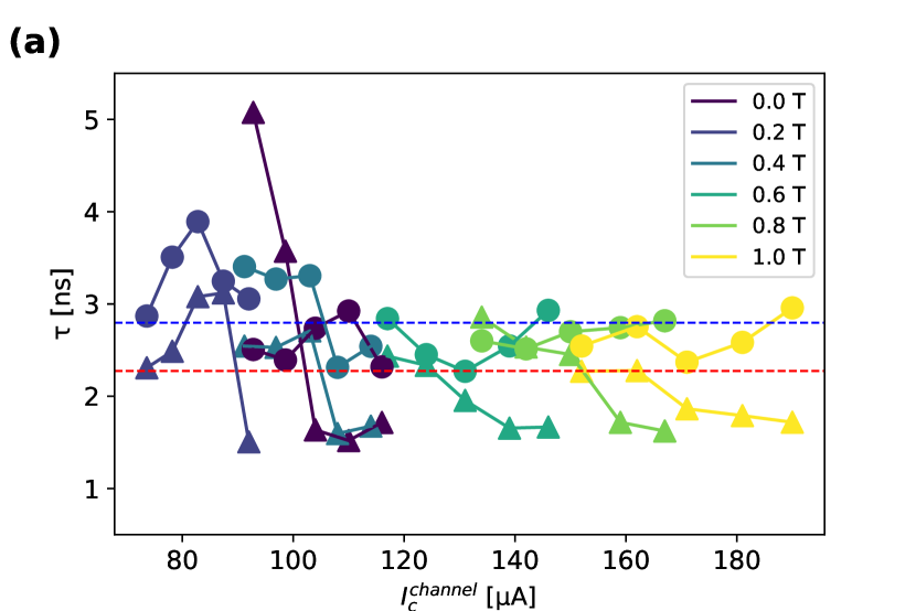
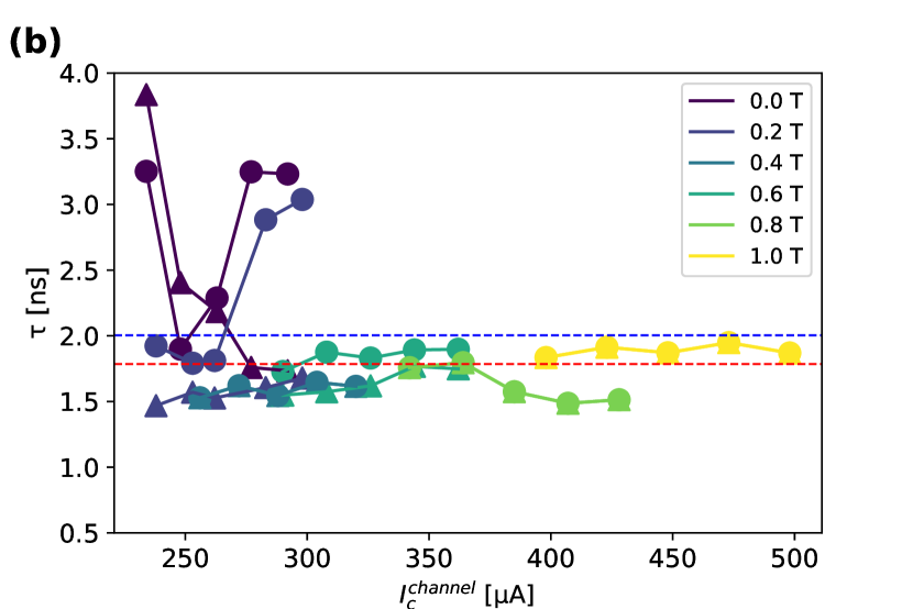
Conversely, Fig. 5 shows the recovery speeds of the conventional nTrons. The 1:2 device demonstrates a slower speed on average when compared to its gapped counterpart by 0.5 ns (double) and 1.61 ns (step) between the two pulse methods. Whilst, the larger 1:8 scale design only shows an average increase of 0.29 ns (step) and notably a decrease of -0.19 ns (double) in between the two methods. There is large variation at 0 and 0.2 T derived from the stochastic nature of the switching seen in the DC characteristics, but is otherwise consistent between both pulsing techniques. Table 2 indicates the averages of each technique for all devices including the difference between the gapped and conventional design.
| Ratio | 1:2 (ns) | 1:8 (ns) | ||||
|---|---|---|---|---|---|---|
| Gapped | Conv. | Gapped | Conv. | |||
| Double | 1.77 | 2.27 | 0.50 | 1.97 | 1.78 | 0.19 |
| Step | 1.19 | 2.80 | 1.61 | 1.71 | 2.00 | 0.29 |
In summary, our study demonstrates larger-size NbN nTron operation through the introduction of parallel connection of multiple channels, increasing the effective channel width. These modifications reduce stochastic switching events, enhance gate signal sensitivity, and promote vortex pinning which helps reduce false signal noise, particularly at higher bias currents. While reducing the channel width has a minimal impact on recovery times of the 1:8 devices with wider aspect ratios, the smaller 1:2 ratio design exhibits enhanced recovery speeds on average as fast as 1.19 ns compared to its conventional counterpart of 2.80 ns, making it suitable for on-chip integration with other superconducting circuitry like SNSPDs. Future work may involve adjusting channel gap sizes and length in 1:2 ratio designs to further optimize gate sensitivity at higher bias currents and improve recovery times at high current gains.
See the supplementary material for SEM images of nTrons (Fig. S1), DC channel and gate switching current characterization scans (Fig. S2-7 and Table S1-3), and recovery time pulse parameters (Table S4-5).
Acknowledgements.
This work was supported by the U. S. Department of Energy (DOE), Office of Science, Office of Nuclear Physics, Microelectronics Initiative, under Contract No. DE-AC02-06CH11357. Y. L. acknowledges support by the U.S. DOE, Office of Science, Office of Basic Energy Sciences, Materials Sciences and Engineering Division under Contract No. DE-SC0022060. Work performed at the Center for Nanoscale Materials, a U.S. Department of Energy Office of Science User Facility, was supported by the U.S. DOE, Office of Basic Energy Sciences, under Contract No. DE-AC02-06CH11357.Author Declarations
Conflict of Interest
The authors have no conflicts to disclose.
Author Contributions
Timothy Draher: Conceptualization (equal); Data curation (lead); Formal analysis (lead); Investigation (lead); Methodology (equal); Resources (supporting); Software (lead); Validation (equal); Visualization (lead); Writing - original draft (lead); Writing - review and editing (lead). Tomas Polakovic: Conceptualization (lead); Formal analysis (equal); Methodology (lead); Project Administration (equal); Resources (supporting); Software (supporting); Supervision (equal); Validation (lead); Visualization (supporting); Writing - original draft (supporting); Writing - review and editing (supproting); Yi Li: Methodology (supporting); Supervision (supporting); Validation (supporting). John Pearson: Supervision (supporting). Alan Dibos: Methodology (supporting); Resources (supporting). Zein-Eddine Meziani: Project Administration (supporting); Supervision (supporting). Zhili Xiao: Supervision (supporting). Valentine Novosad: Funding acquisition (lead); Methodology (supporting); Project administration (lead); Resources (lead); Supervision (equal); Validation (equal);
Data Availability
The data that support the findings of this study are available within the article and its supplementary material.
References
References
- Buck (1956) D. A. Buck, “The cryotron-a superconductive computer component,” Proceedings of the IRE 44, 482–493 (1956).
- McCaughan and Berggren (2014) A. N. McCaughan and K. K. Berggren, “A superconducting-nanowire three-terminal electrothermal device,” Nano Letters 14, 5748–5753 (2014).
- Tanaka et al. (2017) M. Tanaka, M. Suzuki, G. Konno, Y. Ito, A. Fujimaki, and N. Yoshikawa, “Josephson-cmos hybrid memory with nanocryotrons,” IEEE Transactions on Applied Superconductivity 27, 1–4 (2017).
- Zhao et al. (2017) Q.-Y. Zhao, A. N. McCaughan, A. E. Dane, K. K. Berggren, and T. Ortlepp, “A nanocryotron comparator can connect single-flux-quantum circuits to conventional electronics,” Superconductor Science and Technology 30, 044002 (2017).
- Zhao et al. (2018) Q.-Y. Zhao, E. A. Toomey, B. A. Butters, A. N. McCaughan, A. E. Dane, S.-W. Nam, and K. K. Berggren, “A compact superconducting nanowire memory element operated by nanowire cryotrons,” Superconductor Science and Technology 31, 035009 (2018).
- McCaughan et al. (2019) A. N. McCaughan, V. B. Verma, S. M. Buckley, J. P. Allmaras, A. G. Kozorezov, A. N. Tait, S. W. Nam, and J. M. Shainline, “A superconducting thermal switch with ultrahigh impedance for interfacing superconductors to semiconductors,” Nature Electronics 2, 451–456 (2019).
- Zheng et al. (2020) K. Zheng, Q.-Y. Zhao, H.-Y.-B. Lu, L.-D. Kong, S. Chen, H. Hao, H. Wang, D.-F. Pan, X.-C. Tu, L.-B. Zhang, X.-Q. Jia, J. Chen, L. Kang, and P.-H. Wu, “A superconducting binary encoder with multigate nanowire cryotrons,” Nano Letters 20, 3553–3559 (2020).
- Krylov and Friedman (2019) G. Krylov and E. G. Friedman, “Sense amplifier for spin-based cryogenic memory cells,” IEEE Transactions on Applied Superconductivity 29, 1–4 (2019).
- Huang et al. (2023) Y.-H. Huang, Q.-Y. Zhao, S. Chen, H. Hao, H. Wang, J.-W. Guo, X.-C. Tu, L.-B. Zhang, X.-Q. Jia, J. Chen, L. Kang, and P.-H. Wu, “Splitter trees of superconducting nanowire cryotrons for large fan-out,” Applied Physics Letters 122 (2023), 10.1063/5.0139791.
- Polakovic et al. (2020) T. Polakovic, W. Armstrong, G. Karapetrov, Z.-E. Meziani, and V. Novosad, “Unconventional applications of superconducting nanowire single photon detectors,” Nanomaterials 10, 1198 (2020).
- Khalek et al. (2022) R. A. Khalek, A. Accardi, J. Adam, D. Adamiak, W. Akers, M. Albaladejo, A. Al-Bataineh, M. Alexeev, F. Ameli, P. Antonioli, et al., “Science requirements and detector concepts for the electron-ion collider: Eic yellow report,” Nuclear Physics A 1026, 122447 (2022).
- Marsili et al. (2011) F. Marsili, F. Najafi, E. Dauler, F. Bellei, X. Hu, M. Csete, R. J. Molnar, and K. K. Berggren, “Single-photon detectors based on ultranarrow superconducting nanowires,” Nano letters 11, 2048–2053 (2011).
- Il’in et al. (2005) K. Il’in, M. Siegel, A. Semenov, A. Engel, and H. Hübers, “Critical current of nb and nbn thin-film structures: The cross-section dependence,” physica status solidi (c) 2, 1680–1687 (2005).
- Kerman et al. (2009) A. J. Kerman, J. K. W. Yang, R. J. Molnar, E. A. Dauler, and K. K. Berggren, “Electrothermal feedback in superconducting nanowire single-photon detectors,” Physical Review B 79, 100509 (2009).
- Kerman et al. (2006) A. J. Kerman, E. A. Dauler, W. E. Keicher, J. K. W. Yang, K. K. Berggren, G. Gol’tsman, and B. Voronov, “Kinetic-inductance-limited reset time of superconducting nanowire photon counters,” Applied Physics Letters 88 (2006), 10.1063/1.2183810.
- Toomey et al. (2018) E. Toomey, Q.-Y. Zhao, A. N. McCaughan, and K. K. Berggren, “Frequency pulling and mixing of relaxation oscillations in superconducting nanowires,” Physical Review Applied 9, 064021 (2018).
- Annunziata et al. (2010) A. J. Annunziata, O. Quaranta, D. F. Santavicca, A. Casaburi, L. Frunzio, M. Ejrnaes, M. J. Rooks, R. Cristiano, S. Pagano, A. Frydman, and D. E. Prober, “Reset dynamics and latching in niobium superconducting nanowire single-photon detectors,” Journal of Applied Physics 108 (2010), 10.1063/1.3498809.
- Polakovic et al. (2018) T. Polakovic, S. Lendinez, J. E. Pearson, A. Hoffmann, V. Yefremenko, C. L. Chang, W. Armstrong, K. Hafidi, G. Karapetrov, and V. Novosad, “Room temperature deposition of superconducting niobium nitride films by ion beam assisted sputtering,” APL Materials 6, 76107 (2018).
- Clem and Berggren (2011) J. R. Clem and K. K. Berggren, “Geometry-dependent critical currents in superconducting nanocircuits,” Physical Review B 84, 174510 (2011).
- Inoue et al. (2019) M. Inoue, K. Izaki, Y. Goto, K. Sano, T. Yamashita, M. Tanaka, and A. Fujimaki, “Fundamental study on the nanocryotron properties by the numerical calculation,” IEEE Transactions on Applied Superconductivity , 1–1 (2019).
- Brenner et al. (2012) M. W. Brenner, D. Roy, N. Shah, and A. Bezryadin, “Dynamics of superconducting nanowires shunted with an external resistor,” Physical Review B 85, 224507 (2012).
- Bulaevskii et al. (2011) L. N. Bulaevskii, M. J. Graf, C. D. Batista, and V. G. Kogan, “Vortex-induced dissipation in narrow current-biased thin-film superconducting strips,” Physical Review B 83, 144526 (2011).
- Kitaygorsky et al. (2007) J. Kitaygorsky, I. Komissarov, A. Jukna, D. Pan, O. Minaeva, N. Kaurova, A. Divochiy, A. Korneev, M. Tarkhov, B. Voronov, I. Milostnaya, G. Gol’tsman, and R. Sobolewski, “Dark counts in nanostructured nbn superconducting single-photon detectors and bridges,” IEEE Transactions on Applied Superconductivity 17, 275–278 (2007).
- Colauto, Motta, and Ortiz (2021) F. Colauto, M. Motta, and W. A. Ortiz, “Controlling magnetic flux penetration in low-t c superconducting films and hybrids,” Superconductor Science and Technology 34, 013002 (2021).
- Wang et al. (2013) Y. L. Wang, M. L. Latimer, Z. L. Xiao, R. Divan, L. E. Ocola, G. W. Crabtree, and W. K. Kwok, “Enhancing the critical current of a superconducting film in a wide range of magnetic fields with a conformal array of nanoscale holes,” Physical Review B 87, 220501 (2013).
- Karapetrov et al. (2012) G. Karapetrov, V. Yefremenko, G. Mihajlović, J. E. Pearson, M. Iavarone, V. Novosad, and S. D. Bader, “Evidence of vortex jamming in abrikosov vortex flux flow regime,” Physical Review B 86, 054524 (2012).
- Reichhardt and Reichhardt (2010) C. J. O. Reichhardt and C. Reichhardt, “Commensurability, jamming, and dynamics for vortices in funnel geometries,” Physical Review B 81, 224516 (2010).
- Zheng et al. (2019) K. Zheng, Q.-Y. Zhao, L.-D. Kong, S. Chen, H.-Y.-B. Lu, X.-C. Tu, L.-B. Zhang, X.-Q. Jia, J. Chen, L. Kang, and P.-H. Wu, “Characterize the switching performance of a superconducting nanowire cryotron for reading superconducting nanowire single photon detectors,” Scientific Reports 9, 16345 (2019).