Observation of strong attenuation within the photonic band gap of multiconnected networks
Abstract
We theoretically and experimentally study a photonic band gap (PBG) material made of coaxial cables. The coaxial cables are waveguides for the electromagnetic waves and provide paths for direct wave interference within the material. Using multiconnected coaxial cables to form a unit cell, we realize PBGs via (i) direct interference between the waveguides within each cell and (ii) scattering among different cells. We systematically investigate the transmission of EM waves in our PBG materials and discuss the mechanism of band gap formation. We observe experimentally for the first time the wide band gap with strong attenuation caused by direct destructive interference.
I Introduction
Dielectric structures with dielectric constants arranged periodically on the wavelength scale can exhibit photonic band gaps (PBGs), in which the propagation of electromagnetic (EM) waves are inhibited [1, 2]. When an incident wave enters a PBGs, it decays rapidly, forming an attenuation mode, a property that is of great importance for the modulation of EM waves [3, 4, 5]. Photonic crystals are conventional PBG materials with PBGs and have attracted large interests both theoretically and experimentally [6, 7, 8, 9, 10, 11, 12, 13, 14, 15, 16]. However, direct measurement of EM waves in photonic crystals is challenging [4, 17, 18, 13].
A periodic network structure consisting of waveguides has been proposed and localization of states have been observed inside this material [19, 20]. Such a waveguide network essentially introduces resonant loops, which can be resonated and antiresonated in a certain frequency range [19, 20, 21, 22]. In particular, the waveguide network made of coaxial cables is easy to implement in experiments and allows for a more intuitive study of the EM wave transmission inside the structure, as the amplitude and phase changes of the nodes in each part of the network can be better measured, which will allow for further in-depth study and understanding of the EM wave behavior in the PBGs [19, 22, 20, 21].
It is also convenient to modify the network structure to have interesting features. For example, it was theoretically found that the use of multiple waveguides to connect the same pair of nodes in the network can lead to strong attenuation of the wave propagation within the PBGs [23]. This motivates further theoretical studies in various structures with interesting properties [24, 25, 26, 27]. Optical waveguide networks can produce rich photon attenuation modes [28], interesting comb optical transmission spectra [29, 30], extremely wide PBGs [23, 12, 21], super-photon localization [31, 32, 28, 24]. Some of the properties of optical waveguides are applied to microcantilever sensor [33], passive optical device [34], and the physics of -symmetry can also be investigated in it [35, 36, 37, 38].
In this paper, we experimentally design a one-dimensional (1D) networks system constructed from coaxial cables, where multiple cables are used to realize different paths for the EM waves such that the EM waves can have direct interference within each unit cell [see Fig. 1]. Changing the relative length ratios of the coaxial cables, we find that direct destructive interference between different paths leads to a very wide PBG. Within this wide band gap, the propagation of EM wave is strongly prohibited. Remarkably, under certain conditions, the incident EM wave in a PBG can not travel through even one unit cell and are almost totally reflected at the boundary of the material, because of the strong attenuation caused by direct interference.
The paper is organized as follows: Section II describes the modeling and methodology used to study our PBG material as well as our experimental setup. Section III investigates the energy band structure and attenuation characteristics of our material. We draw our conclusions in Sec. IV.
II Model, Theory, and Methods
II.1 Network Structure
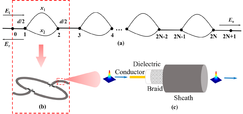
Fig. 1(a) is a schematic structure of our PBG material made of connected waveguides containing unit cells. In each cell there are two connected waveguides with lengths and for direct interference, and these interference structures are linked by waveguides of a length . We use coaxial cables to realize the waveguides for EM waves. Fig. 1(b) illustrates a unit cell in which the cables are connected to each other by connectors. The ports of the connectors can be used to measure the amplitudes of the EM waves. Fig. 1(c) shows the structure of a coaxial cable, which consists of a center conductor, a layer of insulating material, a mesh fabric shield, and an outer sheath.
Compared with traditional photonic crystals, the structure of our networks is easier to realize; the use of coaxial cables is more flexible from the measurement point of view. In photonic crystals, EM waves are measured mainly on the surface of the material [4, 16, 20], whereas in the waveguide networks, one can measure the phase and amplitude of EM waves inside any unit cells, thus bringing convenience to experimental studies.
II.2 Transmission line networks
Pictures of our experimental samples are shown in Fig. 2, with Fig. 2(a) showing a network system consisting of 5 unit cells. The connectors used for our experiments are shown in Fig. 2(b). The red ports of the connector are used to connect the upper and lower arms of the interference structure in each unit cell, while the blue ports are used to connect the interference structures of successive unit cells or for measurement of the EM waves. In our experiments, we used a coaxial cable (type RG58C/U) with the waveguide length shown in Fig. 2(c). The details of the cable-node connection can be seen in the single-cycle unit cell formed by the connectors and the cables, as shown in Fig. 2(d).

II.3 Equations for transmission line networks with single materials
For our networks system shown in Fig. 1,the propagation of EM waves in a coaxial cable line satisfies the following homogeneous wave equation [20, 21]:
| (1) |
where denotes the voltage wave function of any segment between nodes and , is the distance measured from node , is the angular frequency of EM wave, is the wave speed of EM wave in vacuum, is the relative permittivity of the dielectric for the coaxial cables, and and are the real and imaginary parts of the relative permittivity, respectively. The EM wave function can be written as a linear combination of two plane waves traveling in opposite directions [21, 23, 39, 25, 31]:
| (2) |
where is the imaginary unit, [20, 21]. In the case of , it is deduced that has the simple form that , where and is the absorption length. For any node of the network, its wave function is continuous at the node [21, 23, 32, 25, 31]:
| (5) |
where and represent the wavefunction at the nodes and , respectively. is the length of a waveguide connecting the nodes and . With the use of Eqs. (2) and (5), one obtains [25, 31, 32]:
| (6) |
At each node , the wave function is continuous and the derivative of the wave function at node gives the flux conservation condition [23, 25, 32]:
| (7) |
where is the sum of all nodes directly connected to . Substituting Eq. (6) into Eq. (7), one gets [19, 20, 21, 39, 25, 23, 31]:
| (8) |
for the network consisting of coaxial cables without considering dissipation. The coth and sinh denote hyperbolic tangent and hyperbolic sine functions, respectively. We have added a constant to the term of Eq. (8) to account for the additional losses caused by the connectors if we consider the dissipation of the material.
We obtain the absorption length of the cables and the attenuation of the connectors by using the calculated transmission coefficients which fit the measured transmission coefficients in a single cell. Using the cable specifications given by the vendor, as well as our experimental measurements and data fitting, we obtained and . We used .
Therefore, the transmission coefficient theoretically is calculated using the generalized eigenfunction method to solve the equation, where is the transmission amplitude of the outgoing wave. The transmittance is [25, 31, 32, 39, 21].
II.4 Generalized Floquet-Bloch ’s Theorem
The network equation describes the connection relationship between adjacent nodes in a network. In order to quantitatively analyze the energy bands of the system, we derive the dispersion relation of the network structure. To tackle the problem that in our network system the length of a unit cell is not well defined when the same pair of nodes in the unit cell are connected with cables of different lengths, we use the generalized version of the Floquet-Bloch theorem with the following Bloch function [23, 39, 25, 31, 32]:
| (9) |
where the integer denotes an arbitrarily node index, the integer is the period of the network configuration, and is a dimensionless phase factor. For the 0, 2, and 4 nodes in Fig. 1, it follows from Eq. (8):
| (10) |
From Eq. (9), the wave functions at node 0 and node 4 are related to the wave function at node 2 as [23, 24, 32]:
| (13) |
Substituting Eq. (13) into Eq. (10) gives
| (14) |
where
| (18) |
From Eq. (14) we obtain the band structure of our networks. Because of Eq. (9), when the solution is a complex number with a non-zero imaginary part , the propagation of EM wave among the network nodes has a decay rate given by the amplitude of . That is, we have a band gap when has no real solution in Eq. (14). When the amplitude of is larger, the propagation of EM wave among the network nodes has a stronger attenuation. On the other hand, a real solution corresponds to a propagation mode among the network nodes. Therefore, we obtain the dispersion relation for the energy bands from the existence of solutions with a real [23].
III Results and discussion
III.1 Observation of large PBGs
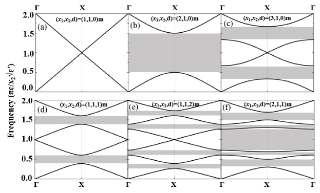
The structure of our network allows us to tune the interference effect between the two arms by changing the lengths and (see Fig. 1). Without lost of generality, we assume . Furthermore, changing the length of the cables that connect the interference structures together, we can also modify the scattering among different cells. From Eq. (14) and Fig. 3, we can see that the band structure changes with the ratio between and as well as the length . The forbidden bands are indicated by gray areas in Fig. 3. As demonstrated in Fig. 3, the ratio between the lengths and of the two arms has a large influence on the PBGs [23, 24, 25].
For the case of there is no destructive interference, and therefore when there is no PBG. When there are small PBGs even , which is due to scattering among different cells. When , there is a strong destructive interference, and as a consequence, a large band gap is formed.
III.2 Experimental demonstration of transmittance
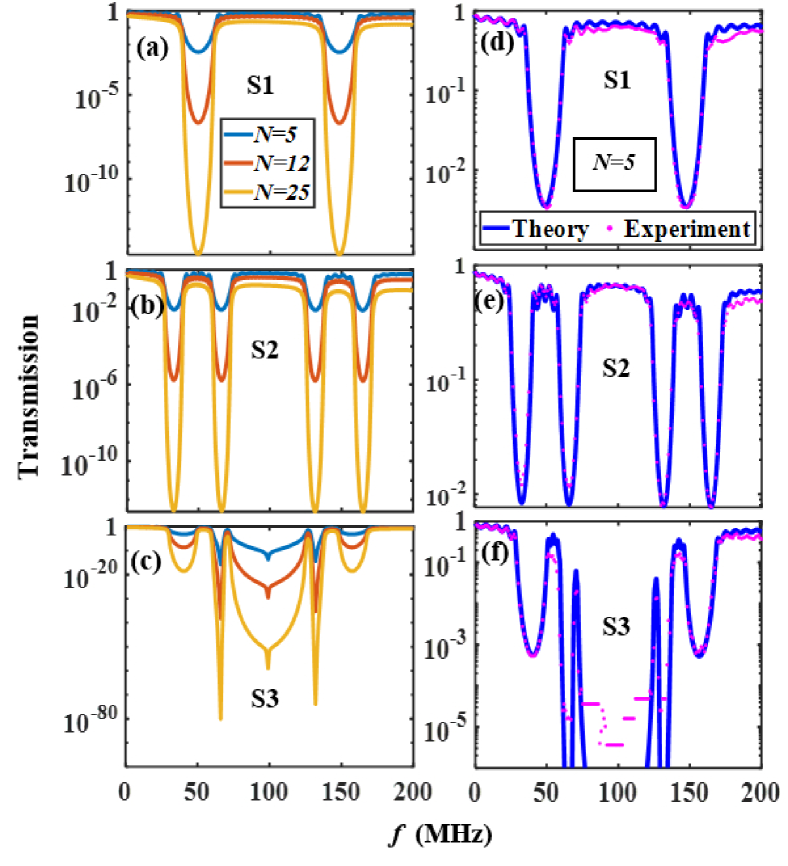
To experimentally probe the system, we connected an Agilent E4438C vector signal generator at one side of the network to input voltage waves. An oscilloscope was connected at the other side of the network to measure the transmission coefficients and intensities. Based on the theoretical results shown in Fig. 1, we prepared different samples of the networks with three different sets of parameters, namely, Structure 1 (S1) with m, S2 with m, and S3 with m.
The experimentally measured transmittance , as well as the theoretically calculated values for the networks S1, S2 and S3 are shown in Fig. 4. The results in Fig. 4 show that the transmittance at the PBGs is getting smaller for a larger size of the network. It is more interesting to see that the attenuation of EM waves within the PBGs is significantly larger for the network S3, which has the ratio , when comparing with other networks S1 and S2 which have . This shows that the destructive interference between the two arms and significantly enhances the formation of PBGs. The results are consistent with the band structures in Fig. 3.
III.3 Wave Intensity Distribution at Characteristic Frequencies
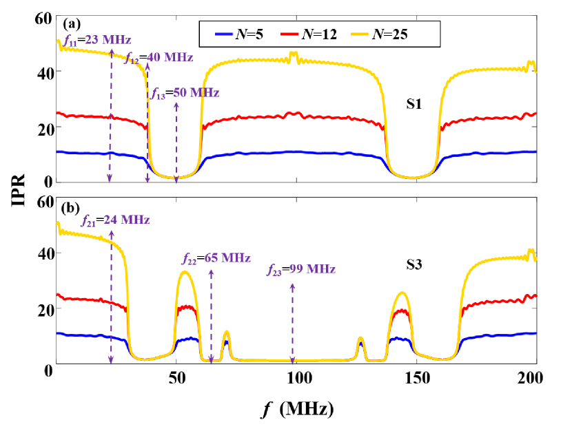
In order to investigate the propagation modes of EM waves, we have systematically probed the S1 and S3 networks with various periods , 12, and 25. Firstly, we use the inverse participation ratio [40, 20, 39]:
| (19) |
to investigate the wave intensity distribution. For the propagation modes, the value of IPR increases with the size (i.e., ) of the network [20]. While for the case that the frequency of a EM wave lying within a PBG, the value of IPR hardly changes with the network size.
We plot the IPR spectral distributions in Fig. 5, where we can see that for frequencies near the band edge, IPR increases with the size of the networks. As the frequency enters the gap, the IPR becomes smaller and the size dependence becomes smaller.
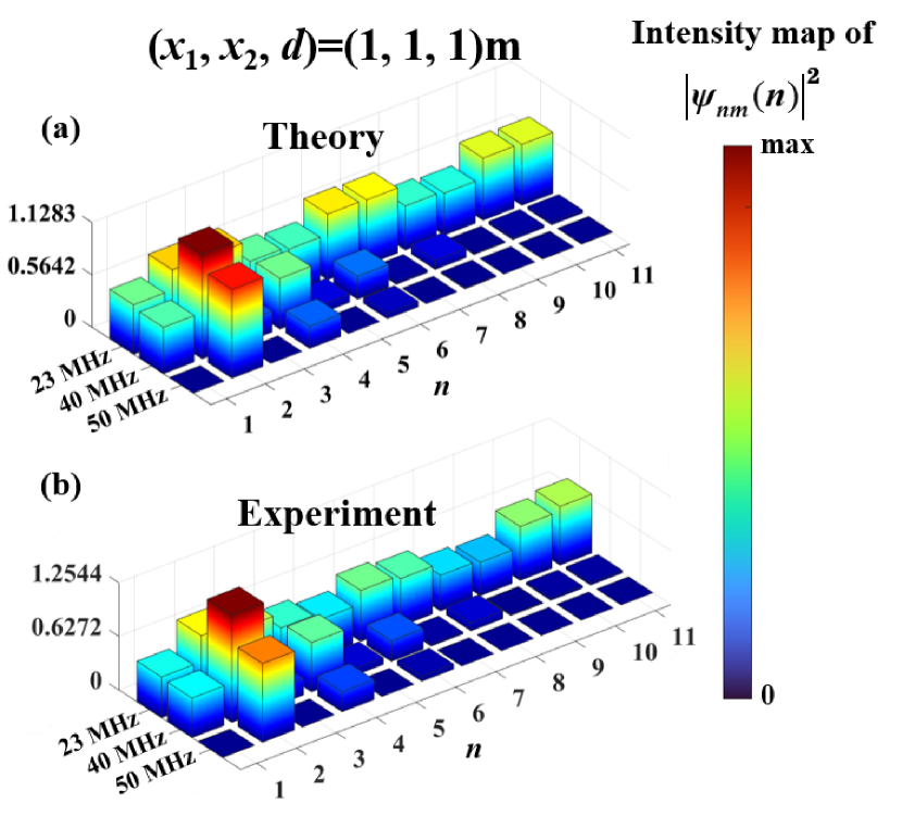
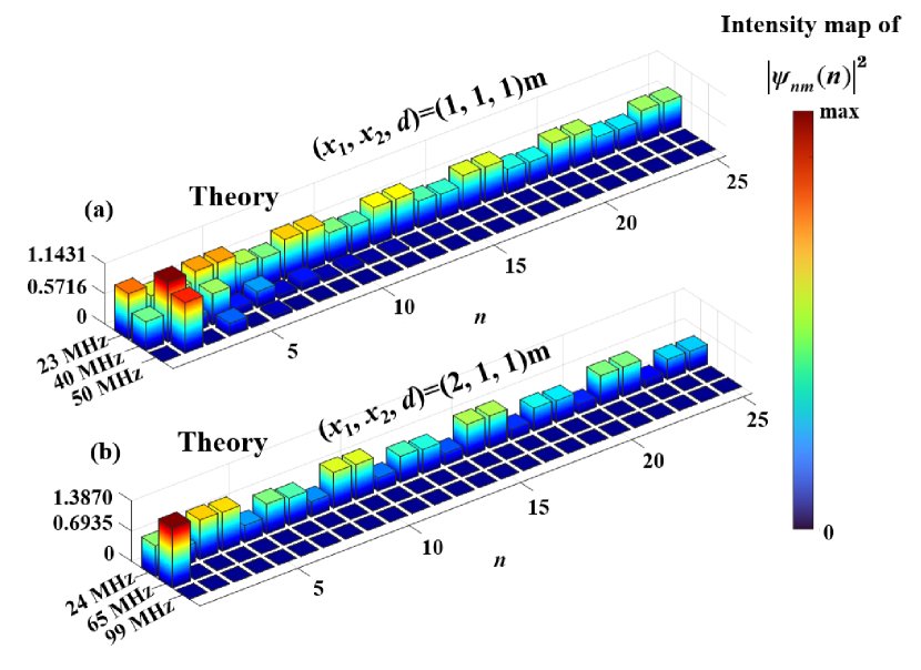
To have a clear picture of the EM wave distribution inside the network, we further conducted experiments to measure the intensities of the EM waves of all the nodes in the networks, for the EM wave frequencies indicated in Fig. 5. We show in Figs. 6 and 7 the voltage intensities of all the nodes for the networks S1 (with ) and S3 (with ), respectively. One can see that the theoretical results agree with the experimental values. The results show that at the frequencies when the IPR increases with the network size , the energy of EM wave have a broad distribution, which indicates an extended state. At the frequencies when the IPR is not sensitive to the network size, the intensities are negligible over a broad range of nodes, which suggests an evanescent mode [28].
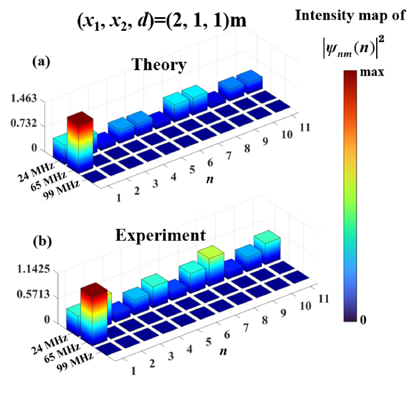
Note that as we can see in Fig. 7 for the network S3, which has , an ultra strong attenuation of EM wave within a PBG is observed. In particular, for the frequency MHz close to the center of the PBG, all the nodes within the network have negligible intensities, because the amplitude of the attenuation mode attenuates to zero even within the first unit cell and all the EM wave energy is reflected at the input side. This ultra strong attenuation is due to the direct destructive interference between the two arms of lengths and . For the network S1, which has , the attenuation of EM wave within PBGs is weaker, when one compares the results in Figs. 6 and 7 as well as the plots in Fig. 8.
The results show that the PBG due to direct interference between the waveguides within each cell is quite different from the conventional PBGs due to scattering among different cells and provides a much stronger attenuation of EM waves.
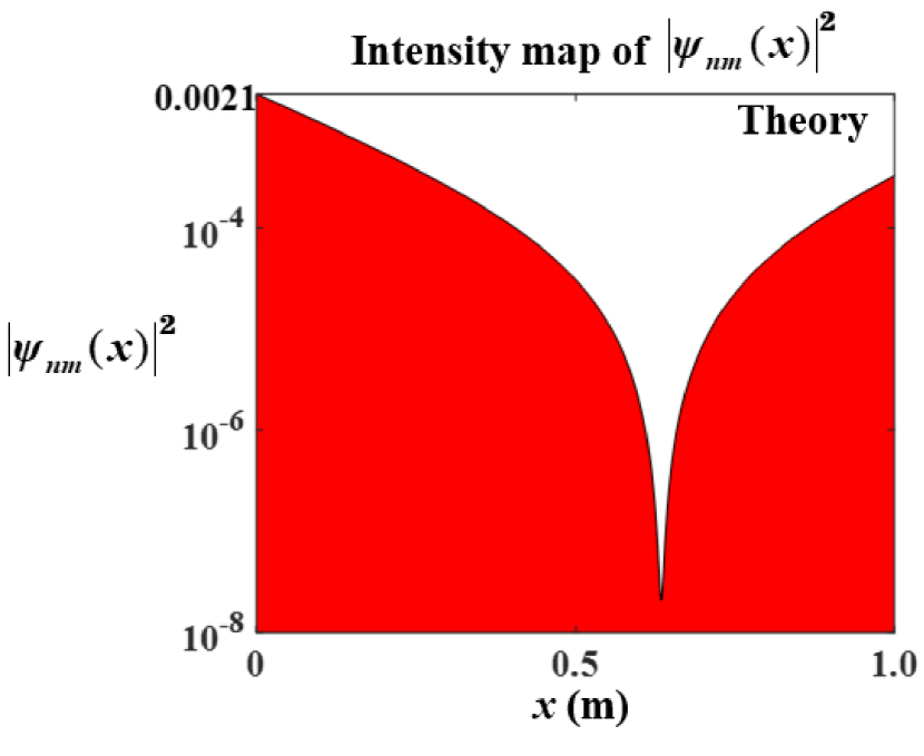
To further investigate the strong attenuation mechanism of the network of S3 at the frequency MHz, in Fig. 9 we calculated the wave intensity distribution between the signal generator output and the first contact of the network using the theory of Eq. (6). We find that the wave intensities in the coaxial cable from the signal output to the first node of the network are all less than 0.0021. Meanwhile, we performed experimental verification and found that the voltage waves are indeed attenuated rapidly in the first section of the coaxial cable. It is clear that this is not due to the geometric scattering structure in the network, but is the result of the interference between the incident and reflected waves in a single coaxial cable.
IV Conclusions
We have theoretically and experimentally study a PBG material made of multiconnected coaxial cables. We have observed for the first time large PBGs which is due to direct wave interference within each unit cell. From the measured transmission spectra and intensities of EM waves inside the networks, we found that direct interference between two waveguides within the same unit cell provides a new mechanism of PBG formation. In particular, when the length ratio between the two arms , a PBG with ultra strong attenuation of EM waves is formed due to direct destructive interference. The strong attenuation within the PBG induces an ultra strong reflection of EM waves at the boundary of the network. Our results demonstrate a new way to realize PBGs and may have applications to the control of various waves (e.g., EM waves or acoustic waves). It would also be interesting to study how the multiconnected waveguides would influence the topological transport in transmission line network [41].
Acknowledgements.
This work was supported by the National Natural Science Foundation of China (Grant Numbers 11674107, 61475049, 11775083, 61774062, 61771205, 12074131) and the Natural Science Foundation of Guangdong Province, China (Grant No. 2021A1515012030).References
- Yablonovitch [1987] E. Yablonovitch, Inhibited spontaneous emission in solid-state physics and electronics, Phys. Rev. Lett. 58, 2059 (1987).
- John [1987] S. John, Strong localization of photons in certain disordered dielectric superlattices, Phys. Rev. Lett. 58, 2486 (1987).
- Askitopoulos et al. [2011] A. Askitopoulos, L. Mouchliadis, I. Iorsh, G. Christmann, J. J. Baumberg, M. A. Kaliteevski, Z. Hatzopoulos, and P. G. Savvidis, Bragg polaritons: Strong coupling and amplification in an unfolded microcavity, Phys. Rev. Lett. 106, 076401 (2011).
- Felbacq and Smaâli [2004] D. Felbacq and R. Smaâli, Bloch modes dressed by evanescent waves and the generalized goos-hänchen effect in photonic crystals, Phys. Rev. Lett. 92, 193902 (2004).
- Armenise et al. [2010] M. N. Armenise, C. E. Campanella, C. Ciminelli, F. Dell’Olio, and V. M. Passaro, Phononic and photonic band gap structures: modelling and applications, Physics Procedia 3, 357 (2010).
- Povinelli et al. [2001] M. L. Povinelli, S. G. Johnson, S. Fan, and J. D. Joannopoulos, Emulation of two-dimensional photonic crystal defect modes in a photonic crystal with a three-dimensional photonic band gap, Phys. Rev. B 64, 075313 (2001).
- Foteinopoulou [2012] S. Foteinopoulou, Photonic crystals as metamaterials, Physica B Condens. Matter 407, 4056 (2012).
- Lodahl et al. [2004] P. Lodahl, A. Floris van Driel, I. S. Nikolaev, A. Irman, K. Overgaag, D. Vanmaekelbergh, and W. L. Vos, Controlling the dynamics of spontaneous emission from quantum dots by photonic crystals, Nature 430, 654 (2004).
- Pradhan and Watson [1999] R. D. Pradhan and G. H. Watson, Impurity effects in coaxial-connector photonic crystals: A quasi-one-dimensional periodic system, Phys. Rev. B 60, 2410 (1999).
- Haché and Poirier [2002] A. Haché and L. Poirier, Anomalous dispersion and superluminal group velocity in a coaxial photonic crystal: Theory and experiment, Phys. Rev. E 65, 036608 (2002).
- Haché and Poirier [2002] A. Haché and L. Poirier, Long-range superluminal pulse propagation in a coaxial photonic crystal, Appl Phys Lett. 80, 518 (2002).
- Cheung et al. [2004] S.-K. Cheung, T.-L. Chan, Z.-Q. Zhang, and C. T. Chan, Large photonic band gaps in certain periodic and quasiperiodic networks in two and three dimensions, Phys. Rev. B 70, 125104 (2004).
- D’orazio et al. [2003] A. D’orazio, M. D. Sario, V. Petruzzelli, and F. Prudenzano, Photonic band gap filter for wavelength division multiplexer, Opt. Express 11 3, 230 (2003).
- Tufarelli et al. [2012] T. Tufarelli, F. Ciccarello, and M. Kim, Dynamics of spontaneous emission in a single-end photonic waveguide, Phys. Rev. A 87 (2012).
- Ao et al. [2009] X. Ao, Z. Lin, and C. T. Chan, One-way edge mode in a magneto-optical honeycomb photonic crystal, Phys. Rev. B 80, 033105 (2009).
- Fan et al. [2013] Y. Fan, Z. Wei, H. Li, H. Chen, and C. M. Soukoulis, Photonic band gap of a graphene-embedded quarter-wave stack, Phys. Rev. B 88, 241403 (2013).
- Povinelli et al. [2003] M. L. Povinelli, S. G. Johnson, J. D. Joannopoulos, and J. B. Pendry, Toward photonic-crystal metamaterials: Creating magnetic emitters in photonic crystals, Appl Phys Lett 82, 1069 (2003).
- Rao and Hughes [2007] V. S. C. M. Rao and S. Hughes, Single quantum dot spontaneous emission in a finite-size photonic crystal waveguide: Proposal for an efficient “on chip” single photon gun, Phys. Rev. Lett. 99, 193901 (2007).
- Zhang and Sheng [1994] Z.-Q. Zhang and P. Sheng, Wave localization in random networks, Phys. Rev. B 49, 83 (1994).
- Zhang et al. [1998] Z. Q. Zhang, C. C. Wong, K. K. Fung, Y. L. Ho, W. L. Chan, S. C. Kan, T. L. Chan, and N. Cheung, Observation of localized electromagnetic waves in three-dimensional networks of waveguides, Phys. Rev. Lett. 81, 5540 (1998).
- Li et al. [2000] M. Li, Y. Liu, and Z.-Q. Zhang, Photonic band structure of sierpinski waveguide networks, Phys. Rev. B 61, 16193 (2000).
- Ciminelli et al. [2005] C. Ciminelli, F. Peluso, and M. N. Armenise, Parametric analysis of 2d guided-wave photonic band gap structures, Opt. Express 13, 9729 (2005).
- Wang and Yang [2007] Z.-Y. Wang and X. Yang, Strong attenuation within the photonic band gaps of multiconnected networks, Phys. Rev. B 76, 235104 (2007).
- Xu et al. [2021] X. Xu, X. Yang, D. Deng, H. Liu, and Z. Wei, Ultrawide photonic bandgap and ultrastrong photonic localization produced by series of periodic networks, Ann Phys 533, 2000584 (2021).
- Cai et al. [2011] L. Cai, X. Yang, and J. Lu, Large photonic band gap and strong attenuation of multiconnected sierpinski network, J. Electromagn. Waves Appl. 25, 147 (2011).
- Tang et al. [2014] Z. Tang, X. Yang, J. Lu, and C. T. Liu, Super-strong photonic localization in symmetric two-segment-connected triangular defect waveguide networks, Opt. Commun 331, 53 (2014).
- Zheng et al. [2019] J. Zheng, X. Yang, X. Zhang, D. Deng, and H. Liu, Transmission characteristics of one-dimensional periodic optical waveguide networks, Phys. Rev. A 99, 023809 (2019).
- Xu et al. [2015] X. Xu, X. Yang, S. Wang, T. C. yi Liu, and D. Deng, Sufficient condition for producing photonic band gaps in one-dimensional optical waveguide networks, Opt. Express 23 21, 27576 (2015).
- Yang et al. [2013] X. Yang, H. Song, and T. C. Liu, Comb-like optical transmission spectrum resulting from a four-cornered two-waveguide-connected network, Phys. Lett. A 377, 3048 (2013).
- Wang et al. [2014] Y. Wang, X. Yang, J. Lu, G. Zhang, and C. T. Liu, Comb-like optical transmission spectra generated from one-dimensional two-segment-connected two-material waveguide networks optimized by genetic algorithm, Phys. Lett. A 378, 1200 (2014).
- Lu et al. [2012] J. Lu, X. Yang, and L. Cai, Large photonic band gap and strong attenuation of multiconnected peano network, Opt. Commun 285, 459 (2012).
- Xiao et al. [2012] Q. Xiao, X. Yang, J. Lu, and C. Liu, Huge photonic band gaps with strong attenuations resulted from quasi-one-dimensional waveguide networks composed of triangular fundamental loops, Opt. Commun 285, 3775 (2012).
- Jing et al. [2020] Y. Jing, G. Fan, R. Wang, Z. Zhang, M. Wang, X. Cai, J. Wei, X. Chen, H. Li, and Y. Li, Analysis for an improved nanomechanical microcantilever sensor on optical waveguides, IEEE Access 8, 63856 (2020).
- Asnawi et al. [2021] Asnawi, N. A. Siddiq, M. S. Muntini, and Y. H. Pramono, Flexible and low-cost fabrication of optical waveguides based on sno2 for passive optical devices, J. Phys. Conf Ser 1805, 012043 (2021).
- Wu et al. [2019] H. Wu, X. Yang, D. Deng, and H. Liu, Reflectionless phenomenon in -symmetric periodic structures of one-dimensional two-material optical waveguide networks, Phys. Rev. A 100, 033832 (2019).
- Zhi et al. [2018] Y. Zhi, X. Yang, J. Wu, S. Du, P. Cao, D. Deng, and C. T. Liu, Extraordinary characteristics for one-dimensional parity-time-symmetric periodic ring optical waveguide networks, Photon. Res. 6, 579 (2018).
- Wang et al. [2022] Q. Wang, X. Yang, D. Deng, H. Liu, and Z. Wei, Quasi-blackbody, bidirectional super reflection, and new total reflection produced by periodic optical waveguide networks based on three-order -symmetric substructures, Ann Phys 534, 2200207 (2022).
- Wu and Yang [2017] J. Wu and X. Yang, Ultrastrong extraordinary transmission and reflection in pt-symmetric thue-morse optical waveguide networks, Opt. Express 25, 27724 (2017).
- Hu et al. [2017] X. Hu, X. Yang, and D. Deng, Super-strong photonic localizations in symmetric defect waveguide-ring networks, IEEE Photon. J 9, 1 (2017).
- Edwards and Thouless [1972] J. T. Edwards and D. J. Thouless, Numerical studies of localization in disordered systems, J. Phys. C 5, 807 (1972).
- Jiang et al. [2019] T. Jiang, M. Xiao, W.-J. Chen, L. Yang, Y. Fang, W. Y. Tam, and C. T. Chan, Experimental demonstration of angular momentum-dependent topological transport using a transmission line network, Nat. Commun. 10, 434 (2019).