Quantum anomalous Hall state in a fluorinated 1T-MoSe2 monolayer
Abstract
The quantum anomalous Hall state with a large band gap and a high Chern number is significant for practical applications in spintronics. By performing first-principles calculations, we investigate electronic properties of the fully fluorinated 1T-MoSe2 monolayer. Without considering the spin-orbit coupling, the band structure demonstrates single-spin semi-metallic properties and the trigonal warping around valleys. The introduction of the spin-orbit coupling opens considerable band gaps of meV around the two valleys, leading to a nontrivial quantum anomalous Hall state with a Chern number of , which provides two chiral dissipationless transport channels from topological edge states and associated quantized anomalous Hall conductivity. In addition, an effective model is constructed to describe the low-energy physics of the monolayer. Our findings in the MoSe2F2 monolayer sheds light on large-gap quantum anomalous Hall states in two-dimensional materials with the chemical functionalization, and provides opportunities in designing low-power and noise-tolerant spintronic devices.
I Introduction
The quantum anomalous Hall state is a topologically nontrivial state characterized by the quantization of the Hall conductance with nonzero Chern number and chiral edge states, even without the external magnetic field Haldane (1988); Chang et al. (2023). This novel quantum state of matter has been experimentally realized in magnetically doped topological insulators Chang et al. (2013, 2015); Mogi et al. (2015), intrinsic magnetic topological insulators Deng et al. (2020), and moiré materials Serlin et al. (2020); Li et al. (2021a). However, the experimental temperature of realizing the nontrivial state is still low, which brings difficulties to observations and applications. A large nontrivial band gap is thus expected to immune to the influence of temperature, disorder, etc, and increases the experimental temperature Chang et al. (2016). On the other hand, a high Chern number () is desirable to provide multiple topological transport channels. Therefore, the search for the Chern insulator with a large band gap and a high Chern number is vital for practical applications of the quantum anomalous Hall state.
The chemical functionalization is a widely used method to modulate various properties of two-dimensional (2D) materials Kuila et al. (2012); Martín et al. (2020). For examples, the hydrogen functionalizations of graphene and germanane induce a phase transition from a conductive semimetal to an insulator Elias et al. (2009); Li et al. (2021b); the hydrogen and fluorine functionalizations of the stanene monolayer and III-Bi bilayers lead to the quantum spin Hall state with large nontrivial band gaps Xu et al. (2013); Ma et al. (2015); the fluorine functionalization also introduces the magnetism in graphene, BN and MoS2 Feng et al. (2013); Zhang and Guo (2009); Gao et al. (2015). Recently, one of the authors proposed that the fully fluorinated 1T-MoX2 (X=S, Se) monolayer has a stable ferromagnetic order with a high Cuire temperature Wu et al. .
In this paper, by first-principles calculations, we study electronic and topological properties of the fully fluorinated 1T-MoSe2 monolayer, which is abbreviated as MoSe2F2 hereafter. The MoSe2F2 monolayer is a half semi-metal with the trigonal warping around valleys in its electronic band structure, when the spin-orbit coupling is absent. Remarkably, the spin-orbit coupling gives rise to large band gaps of meV near two valleys. By calculating the Chern number and edge states, the quantum anomalous Hall state with is verified in the gapped monolayer. Therefore, a Chern insulator proposed here has a large band gap and multiple conducting channels, which are likely to make the MoSe2F2 monolayer standout among the candidates of the quantum anomalous Hall state. Last but not least, an effective model is provided, and it captures the origin of the band topology of this monolayer. Our work broadens the material choices of the quantum anomalous Hall state, and offers potential applications in designing energy-efficient spintronic devices.
II Methods
The first-principles calculations within the framework of the density functional theory Hohenberg and Kohn (1964); Kohn and Sham (1965) are performed to investigate electronic properties of the MoSe2F2 monolayer, as implemented in Vienna Ab initio Simulation Package Kresse and Furthmüller (1996, 1996). The projected augmented wave method Blöchl (1994) and the Perdew-Burke-Ernzerhof exchange-correlation functionals Perdew et al. (1996) are adopted, with an energy cutoff of 550 eV. A -centered -mesh Monkhorst and Pack (1976) of is used to sample in the first Brillouin zone of the 2D monolayer. A vacuum layer of more than 17 Å is inserted to avoid the interaction between the monolayer and its periodic images, The convergence thresholds of the total energy and the interatomic force on each atom are set to 10-6 eV and eV/Å, respectively. To consider the correlation effects of 3 electrons of Mo atom, the onsite Coulomb corrections Dudarev et al. (1998) are applied with an effective of 3 eV, which gives a similar nonrelativisitic band structure with the HSE06 method Heyd et al. (2003); Wu et al. . The magnified band structures at valleys are obtained by Wannier interpolation via the Wannier90 package Pizzi et al. (2020), which is also used to calculate the Berry curvature and anomalous Hall conductivity.
III Results
III.1 Crystal structure of the MoSe2F2 monolayer
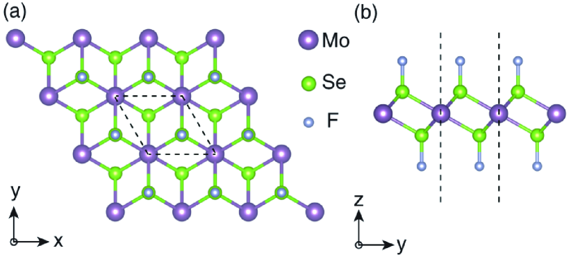
The crystal structure of the MoSe2F2 monolayer is shown in Fig. 1. The MoSe2F2 monolayer has a point group of , with the spatial inversion symmetry and three-fold rotational symmetry. The monolayer exhibits a hexagonal lattice and comprises five atomic layers. The middle three atomic layers are MoSe2 in the T phase, i.e. each molybdenum atom is bonded to six neighboring selenium atoms that form an octahedral environment. The added fluorine atoms reside on the right top (bottom) of the upper (lower) selenium atomic layer. For the MoSe2F2 monolayer, the in-plane lattice constant of the unit cell, , is computed to be 3.94 Å. The distance between the Se and F atoms is 1.82 Å, which is smaller than the sum of the covalent radii of Se (1.16 Å) and F (0.71 Å), indicating the chemical bondings between the Se and absorbed F atoms. The calculation results are consistent with the previous report about the MoSe2F2 monolayer, where its dynamical and thermodynamical stabilities have also been verified by the calculated phonon spectrum and molecular dynamics, respectively Wu et al. . Besides, we calculate the magnetic moment of the ferromagnetic monolayer, which has a magnitude of per unit cell and agrees with the previous work Wu et al. .
III.2 Band structures of the MoSe2F2 monolayer
In the followings, we investigate electronic properties of the MoSe2F2 monolayer, without and with the spin-orbit coupling. Fig. 2(a) shows the band structure without the spin-orbit coupling. Owing to the presence of the ferromagnetic order, all bands are spin polarized. While the spin-up channel is semiconducting with a band gap of eV, the spin-down channel presents a gapless semi-metallic feature with quadratic band touching regions around the Fermi level. The band touching regions are located in the neighborhood of the high-symmetry and points of the momentum space. Therefore, the monolayer is a half semi-metal Cai et al. (2015).
We then focus on the band touching regions around valleys. Given that the monolayer has the spatial inversion symmetry and correspondingly electronic states at valleys are degenerate, we only present the magnified band structures at valley. The magnified band structure is provided along high-symmetry paths in Fig. 2(b). It is seen that the valence and conduction bands indeed have quadratic dispersions. Between the two bands, there are two crossing points, which are located at point and an intermediate point in the - path, respectively. For convenience, the wave vector of the crossing point in the - path is labelled as . The energies of the two crossing points are unequal, with the one at being higher than that at by meV.
Fig. 2(c) further presents the energy difference between the valence and conduction bands over a small 2D region centered at . The energy difference is exactly zero at and . Besides, owing to the presence of the three-fold rotational symmetry, there are three equivalent points along three equivalent - paths, respectively. That is, besides the central crossing point at , there are three satellite crossing points with an angular spacing of around . Moreover, the 3D view of the band structure and the energy contours are given around the valley for both the valence and conduction bands in Supporting Information (SI hereafter), and they support our findings above. According to the energy difference in Fig. 2(c) and energy contours in SI, it is also found that there is a change of the topology of the Fermi surface as the shift of the chemical potential. When moving away from the crossing points, the Fermi surface first includes four pockets centered at and three points, respectively, and then becomes a distorted ring with the trigonal warping. This exotic band structure indicates that the MoSe2F2 monolayer is a potential candidate to investigate the Lifshitz transition of the Fermi surface, by modulating the chemical potential via the carrier doping Volovik (2013, 2017).
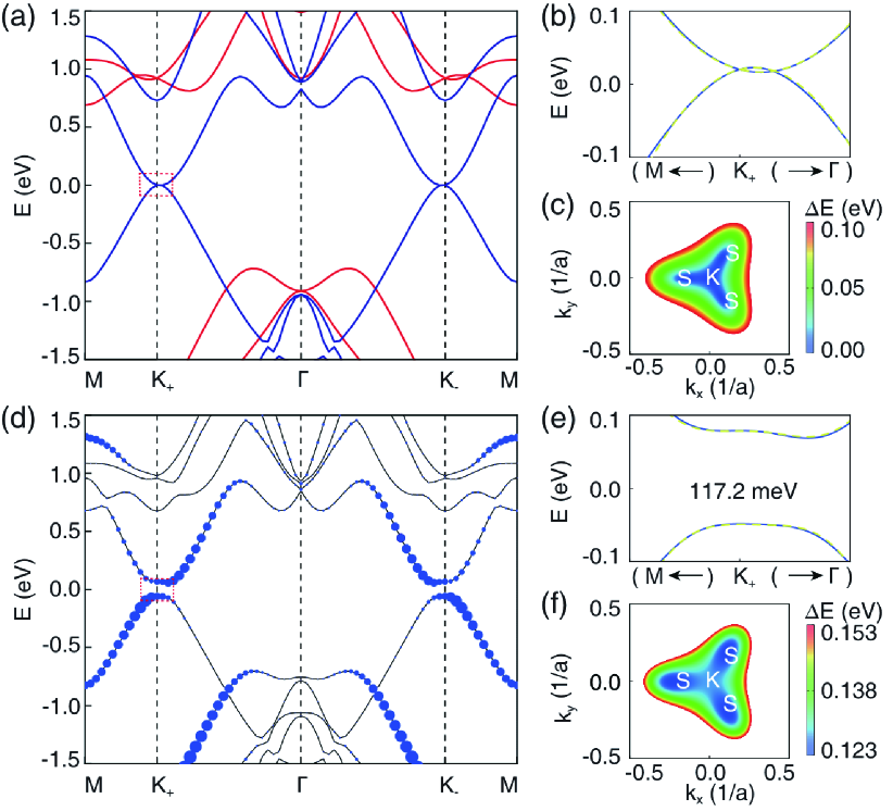
Fig. 2(d) presents the band structures of the MoSe2F2 monolayer with the spin-orbit coupling. The spin-orbit coupling lifts the band touchings between the valence and conduction bands around valleys. Since the conduction band minimum and the valence band maximum are located at different wave vectors, as illustrated in Fig. 2(e), a global indirect band gap appears with a magnitude of meV. At points, the direct band gap has a value of meV. Therefore, the monolayer becomes a semiconductor due to the introduction of the spin-orbit coupling gaps. These band gaps are large enough to survive above the room temperature. Further considering this monolayer is predicted to be a ferromagnet with a Curie temperature of more than 500 K by the Monte Carlo simulation Wu et al. , the magnetic semiconductivity is robust against the ambient temperature.
The energy difference between the valence and conduction bands is also shown in Fig. 2(f) for the band structure with the spin-orbit coupling. The contour of the energy difference exhibits the trigonal warping and the change of the topology of Fermi surface, similar to the above results without the spin-orbit coupling.
III.3 The quantum anomalous Hall state with
Given that the band gaps open in a single-spin channel according to the above calculation results and the band openings are likely to induce the quantum anomalous Hall state, we further investigate topological properties of the MoSe2F2 monolayer. We first calculate the momentum-resolved Berry curvature along the axis, , which is defined as Thouless et al. (1982); Yao et al. (2004); Wang et al. (2006); Xiao et al. (2010),
| (1) |
Here, the Berry curvature includes contributions from all occupied bands below the Fermi level, . is the spinor Bloch wave function of the -th band at the wave vector k, with the corresponding electronic energy denoted as . and are the velocity operators along the and directions, respectively.
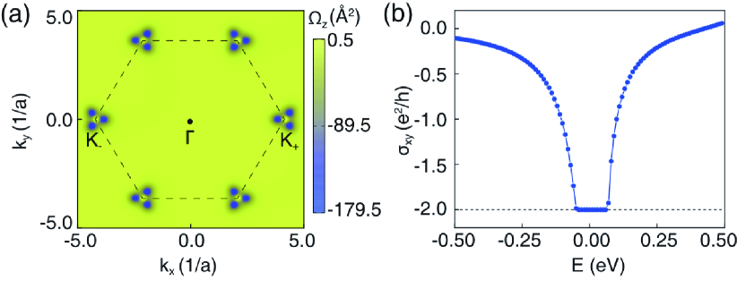
Fig. 3() demonstrates the Berry curvature in the momentum space. The Berry curvature is found to mainly concentrate around and valleys. Due to the inversion symmetry, the Berry curvatures from the two valleys give the same contribution. At each valley, the pattern of Berry curvature shows the clover-leaf shape with the three-fold rotational symmetry, similar to the energy contour of the band structure. It is noted that the pattern is distinct from the single peak of the Berry curvature from massive Dirac cone Xiao et al. (2010). By integrating the Berry curvature in the entire first Brillouin zone, the Chern number of 2D materials can be obtained, i.e. Thouless et al. (1982); Yao et al. (2004); Wang et al. (2006); Xiao et al. (2010). Specific to the MoSe2F2 monolayer, the calculated Chern number is , with the clover-leaf shaped Berry curvature at each valley contributing to a valley Chern number of . The nonzero Chern number indicates the monolayer is indeed a Chern insulator, with a high Chern number. As shown in Fig. 3(b), the high Chern number gives rise to a quantized anomalous Hall conductivity. A Hall plateau of appears, when the chemical potential is within the band gap induced by the spin-orbit coupling.
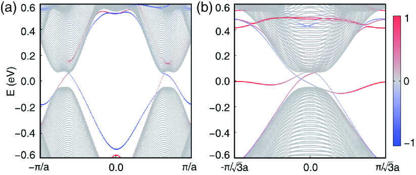
Another important indicator for the Chern insulator is the existence of topologically protected chiral edge states. To further confirm the nontrivial topological properties of the Chern insulator with , the energy spectra of the MoSe2F2 nanoribbons with the zigzag and armchair edges are calculated by the WannierTools package Wu et al. (2018), and they are presented in Fig. 4(a) and 4(b), respectively. Within the band gap, there are topologically nontrivial edge states that seamlessly connect the valence and conduction bands, for both the zigzag and armchair nanoribbons. These gapless edge states can be divided into two groups that are presented by blue and red lines in Fig. 4, respectively. Each group includes two topological edge states. Topological edge states in different groups have opposite group velocities, and they are distributed in opposite edges of the same nanoribbon. The topologically nontrivial edge states support the existence of the quantum anomalous Hall state with .
Moreover, the above results correspond to the magnetization along the axis in the MoSe2F2 monolayer. When the magnetization is reversed to the axis, the Chern number is found to be changed into . Accordingly, the quantized anomalous Hall conductivity becomes , and the chirality of the edge states is reversed.
III.4 The low-energy effective model
To elucidate the origin of the band topology of the MoSe2F2 monolayer, we analyze orbital components of low-energy bands near the Fermi level. It is found that the valence and conduction band edges are mainly contributed by and orbitals of Mo atoms, as shown in Fig. 2(d). Besides, there are also contributions from orbitals of Se and F atoms, which is provided in SI. We then construct the low-energy model at valleys of the monolayer via the MagneticTB package Zhang et al. (2022), using only the (i.e. ) and (i.e. ) orbitals of Mo atoms for simplicity. The low-energy model reads,
| (2) |
Here, is the wave vector with respect to , and . are Pauli matrices for the orbital space, and is the corresponding identity matrix. denote valleys, respectively. is an immaterial global energy shift. - are strength parameters related to onsite energy and hoppings. - and -related terms arise from the spin-orbit coupling, and is equal to the magnitude of the direct band gap at . The low-energy effective model is considered up to the second order in q. It has a similar form with that of the 2H-MoS2 monolayer Kormányos et al. (2013); Liu et al. (2013), but uses different orbital basis sets.
By fitting the first-principles non-relativistic valence and conduction bands via the least squares method, the parameters of the low-energy effective model without considering the spin-orbit coupling are obtained as meV, meVÅ2, meVÅ, meVÅ2. When further considering the spin-orbit coupling, and are fitted to be meVÅ2 and meV, respectively, and becomes meV, while the other parameters are fixed. As shown in Figs. 2(b) and 2(e), with this set of parameters, the band structures from the low-energy effective model and first-principles calculations agree with each other very well. Furthermore, the clover-leaf shaped Berry curvature is also well reproduced, based on our effective model, which is given in SI.
IV Discussions
In the above low-energy model, we consider the first-order and second-order terms in q. It is found that the corresponding parameters are all sizable. Given that the first-order and second-order terms give rise to linear and quadratic band dispersions, respectively, the simultaneous presence of these terms lead to the trigonal warping and the Lifshitz transition of the topology of the Fermi surface in the MoSe2F2 monolayer Volovik (2013, 2017). Correspondingly, the Berry curvature with the clover-leaf shape is also due to these terms. Moreover, by tuning the ratio of to , the band structure and Berry curvature are changed accordingly. In particular, as the ratio is increased, the shape of the Berry curvature at each valley is changed from a ring to a clover leaf, and to a combination of one positive and three negative peaks, which is shown in SI. Therefore, a tunable ratio is expected to be a practical knob to modulate the band structure and Berry curvature. It is likely to be realized by e.g. the strain Ribeiro et al. (2009).
The quantum anomalous Hall state in the MoSe2F2 monolayer is intriguing with outstanding advantages. Firstly, the monolayer has a high ferromagnetic Cuire temperature Wu et al. and a considerable band gap of more than meV, which ensures the robustness of the topological state against the temperature. Secondly, the Chern number of provides more dissipationless conducting channels from topologically nontrivial edge states. Moreover, the comparable linear and quadratic terms in low-energy effective model lead to potential Lifshitz transition, exotic Berry curvatures around valleys, and nontrivial band topology. The mechanism of the band topology is different from the previous reports about other quantum anomalous Hall insulators Qiao et al. (2010); Xu et al. (2011); Fang et al. (2012); Wang et al. (2013); Cai et al. (2015); He et al. (2017); Li et al. (2017, 2019). The MoSe2F2 monolayer provides a new platform for exploring topological quantum states.
It is noted that the fluorination is one of the chemical modifications of the 1T-MoSe2 monolayer. The 1T-MoSe2 monolayer with other decorated atoms, such as hydrogen and iodine atoms, may lead to the ferromagnetic order and the band topology, similar to the MoSe2F2 monolayer. Furthermore, different decorated atoms possibly modulate the linear and quadratic contributions to the low-energy band structure. They are worth further studies.
V Conclusion
To summarize, we have employed the first-principles calculations to study electronic and topological properties of the MoSe2F2 monolayer. In the absence of the spin-orbit coupling, the single-spin valence and conduction bands exhibit half semi-metallic features and the trigonal warping around valleys in electronic band structures. The Lifshitz transition can occur by tuning the chemical potential. More interestingly, the spin-orbit coupling can induce a global band gap of 117.2 meV near the valleys. Accordingly, the quantum anomalous Hall state appears with , which is supported by the calculations of the anomalous Hall conductivity and topological edge states. A two-band low-energy effective model is also provided to better understand the origin of the band topology. The quantum anomalous Hall state in the MoSe2F2 monolayer offers multiple dissipationless transport channels and potential high-temperature applications in spintronics.
Acknowledgements.
We are grateful to Jing Wu for valuable discussions. We are supported by the National Natural Science Foundation of China (Nos. 12004186, 12374044, 11904173). Xiao Li is also supported by the Jiangsu Specially-Appointed Professor Program.References
- Haldane (1988) F. D. M. Haldane, Phys. Rev. Lett. 61, 2015 (1988).
- Chang et al. (2023) C.-Z. Chang, C.-X. Liu, and A. H. MacDonald, Rev. Mod. Phys. 95, 011002 (2023).
- Chang et al. (2013) C.-Z. Chang, J. Zhang, X. Feng, J. Shen, Z. Zhang, M. Guo, K. Li, Y. Ou, P. Wei, L.-L. Wang, Z.-Q. Ji, Y. Feng, S. Ji, X. Chen, J. Jia, X. Dai, Z. Fang, S.-C. Zhang, K. He, Y. Wang, L. Lu, X.-C. Ma, and Q.-K. Xue, Science 340, 167 (2013).
- Chang et al. (2015) C.-Z. Chang, W. Zhao, D. Y. Kim, H. Zhang, B. A. Assaf, D. Heiman, S.-C. Zhang, C. Liu, M. H. W. Chan, and J. S. Moodera, Nature Materials 14, 473 (2015).
- Mogi et al. (2015) M. Mogi, R. Yoshimi, A. Tsukazaki, K. Yasuda, Y. Kozuka, K. S. Takahashi, M. Kawasaki, and Y. Tokura, Applied Physics Letters 107, 182401 (2015).
- Deng et al. (2020) Y. Deng, Y. Yu, M. Z. Shi, Z. Guo, Z. Xu, J. Wang, X. H. Chen, and Y. Zhang, Science 367, 895 (2020).
- Serlin et al. (2020) M. Serlin, C. L. Tschirhart, H. Polshyn, Y. Zhang, J. Zhu, K. Watanabe, T. Taniguchi, L. Balents, and A. F. Young, Science 367, 900 (2020).
- Li et al. (2021a) T. Li, S. Jiang, B. Shen, Y. Zhang, L. Li, Z. Tao, T. Devakul, K. Watanabe, T. Taniguchi, L. Fu, J. Shan, and K. F. Mak, Nature 600, 641 (2021a).
- Chang et al. (2016) C.-Z. Chang, W. Zhao, J. Li, J. K. Jain, C. Liu, J. S. Moodera, and M. H. W. Chan, Phys. Rev. Lett. 117, 126802 (2016).
- Kuila et al. (2012) T. Kuila, S. Bose, A. K. Mishra, P. Khanra, N. H. Kim, and J. H. Lee, Progress in Materials Science 57, 1061 (2012).
- Martín et al. (2020) N. Martín, N. Tagmatarchis, Q. H. Wang, and X. Zhang, Chemistry – A European Journal 26, 6292 (2020).
- Elias et al. (2009) D. C. Elias, R. R. Nair, T. M. G. Mohiuddin, S. V. Morozov, P. Blake, M. P. Halsall, A. C. Ferrari, D. W. Boukhvalov, M. I. Katsnelson, A. K. Geim, and K. S. Novoselov, Science 323, 610 (2009).
- Li et al. (2021b) R. Li, Y. Li, Y. Yang, X. Huang, S. Zhang, H. Tian, X. Huang, Z. Yao, P. Liao, S. Yu, S. Liu, Z. Li, Y. Huang, J. Guo, F. Mei, L. Wang, X. Li, and L. Liu, ACS Applied Nano Materials 4, 13708 (2021b).
- Xu et al. (2013) Y. Xu, B. Yan, H.-J. Zhang, J. Wang, G. Xu, P. Tang, W. Duan, and S.-C. Zhang, Phys. Rev. Lett. 111, 136804 (2013).
- Ma et al. (2015) Y. Ma, X. Li, L. Kou, B. Yan, C. Niu, Y. Dai, and T. Heine, Phys. Rev. B 91, 235306 (2015).
- Feng et al. (2013) Q. Feng, N. Tang, F. Liu, Q. Cao, W. Zheng, W. Ren, X. Wan, and Y. Du, ACS Nano 7, 6729 (2013), publisher: American Chemical Society.
- Zhang and Guo (2009) Z. Zhang and W. Guo, J. Am. Chem. Soc. 131, 6874 (2009), publisher: American Chemical Society.
- Gao et al. (2015) D. Gao, S. Shi, K. Tao, B. Xia, and D. Xue, Nanoscale 7, 4211 (2015).
- (19) J. Wu, R. Guo, D. Wu, X. Li, and X. Wu, arXiv:2310.03995 .
- Hohenberg and Kohn (1964) P. Hohenberg and W. Kohn, Phys. Rev. 136, B864 (1964).
- Kohn and Sham (1965) W. Kohn and L. J. Sham, Phys. Rev. 140, A1133 (1965).
- Kresse and Furthmüller (1996) G. Kresse and J. Furthmüller, Phys. Rev. B 54, 11169 (1996).
- Kresse and Furthmüller (1996) G. Kresse and J. Furthmüller, Computational Materials Science 6, 15 (1996).
- Blöchl (1994) P. E. Blöchl, Phys. Rev. B 50, 17953 (1994).
- Perdew et al. (1996) J. P. Perdew, K. Burke, and M. Ernzerhof, Phys. Rev. Lett. 77, 3865 (1996).
- Monkhorst and Pack (1976) H. J. Monkhorst and J. D. Pack, Phys. Rev. B 13, 5188 (1976).
- Dudarev et al. (1998) S. L. Dudarev, G. A. Botton, S. Y. Savrasov, C. J. Humphreys, and A. P. Sutton, Phys. Rev. B 57, 1505 (1998).
- Heyd et al. (2003) J. Heyd, G. E. Scuseria, and M. Ernzerhof, The Journal of Chemical Physics 118, 8207 (2003).
- Pizzi et al. (2020) G. Pizzi, V. Vitale, R. Arita, S. Blügel, F. Freimuth, G. Géranton, M. Gibertini, D. Gresch, C. Johnson, T. Koretsune, J. Ibañez-Azpiroz, H. Lee, J.-M. Lihm, D. Marchand, A. Marrazzo, Y. Mokrousov, J. I. Mustafa, Y. Nohara, Y. Nomura, L. Paulatto, S. Poncé, T. Ponweiser, J. Qiao, F. Thöle, S. S. Tsirkin, M. Wierzbowska, N. Marzari, D. Vanderbilt, I. Souza, A. A. Mostofi, and J. R. Yates, Journal of Physics: Condensed Matter 32, 165902 (2020).
- Cai et al. (2015) T. Cai, X. Li, F. Wang, S. Ju, J. Feng, and C.-D. Gong, Nano Lett. 15, 6434 (2015).
- Volovik (2013) G. E. Volovik, Lecture Notes in Physics 870, 343 (2013).
- Volovik (2017) G. E. Volovik, Low Temperature Physics 43, 47 (2017).
- Thouless et al. (1982) D. J. Thouless, M. Kohmoto, M. P. Nightingale, and M. den Nijs, Phys. Rev. Lett. 49, 405 (1982).
- Yao et al. (2004) Y. Yao, L. Kleinman, A. H. MacDonald, J. Sinova, T. Jungwirth, D.-s. Wang, E. Wang, and Q. Niu, Phys. Rev. Lett. 92, 037204 (2004).
- Wang et al. (2006) X. Wang, J. R. Yates, I. Souza, and D. Vanderbilt, Phys. Rev. B 74, 195118 (2006).
- Xiao et al. (2010) D. Xiao, M.-C. Chang, and Q. Niu, Rev. Mod. Phys. 82, 1959 (2010).
- Wu et al. (2018) Q. Wu, S. Zhang, H.-F. Song, M. Troyer, and A. A. Soluyanov, Computer Physics Communications 224, 405 (2018).
- Zhang et al. (2022) Z. Zhang, Z. Yu, G. Liu, and Y. Yao, Computer Physics Communications 270, 108153 (2022).
- Kormányos et al. (2013) A. Kormányos, V. Zólyomi, N. D. Drummond, P. Rakyta, G. Burkard, and V. I. Fal’ko, Phys. Rev. B 88, 045416 (2013).
- Liu et al. (2013) G.-B. Liu, W.-Y. Shan, Y. Yao, W. Yao, and D. Xiao, Phys. Rev. B 88, 085433 (2013).
- Ribeiro et al. (2009) R. M. Ribeiro, V. M. Pereira, N. M. R. Peres, P. R. Briddon, and A. H. C. Neto, New Journal of Physics 11, 115002 (2009).
- Qiao et al. (2010) Z. Qiao, S. A. Yang, W. Feng, W.-K. Tse, J. Ding, Y. Yao, J. Wang, and Q. Niu, Phys. Rev. B 82, 161414 (2010).
- Xu et al. (2011) G. Xu, H. Weng, Z. Wang, X. Dai, and Z. Fang, Phys. Rev. Lett. 107, 186806 (2011).
- Fang et al. (2012) C. Fang, M. J. Gilbert, X. Dai, and B. A. Bernevig, Phys. Rev. Lett. 108, 266802 (2012).
- Wang et al. (2013) Z. F. Wang, Z. Liu, and F. Liu, Phys. Rev. Lett. 110, 196801 (2013).
- He et al. (2017) J. He, X. Li, P. Lyu, and P. Nachtigall, Nanoscale 9, 2246 (2017).
- Li et al. (2017) P. Li, X. Li, W. Zhao, H. Chen, M.-X. Chen, Z.-X. Guo, J. Feng, X.-G. Gong, and A. H. MacDonald, Nano Lett. 17, 6195 (2017), publisher: American Chemical Society.
- Li et al. (2019) Y. Li, J. Zhang, B. Zhao, Y. Xue, and Z. Yang, Phys. Rev. B 99, 195402 (2019).