Scanning gate microscopy of non-retracing electron-hole trajectories
in a normal-superconductor junction
Abstract
We theoretically study scanning gate microscopy (SGM) of electron and hole trajectories in a quantum point contact (QPC) embedded in a normal-superconductor (NS) junction. At zero voltage bias, the electrons and holes transported through the QPC create a branched flow and are subject to self-interference, which marks the SGM conductance maps with interference fringes analogously as in normal systems. We predict that for an NS junction at non-zero bias a beating pattern is to occur in the conductance probed with the use of the SGM technique owing to a mismatch of the Fermi wavevectors of electrons and holes. Moreover, the SGM technique exposes a pronounced disturbance in the branched conductance pattern due to wave vector difference, as the retroreflected hole does not retrace the electron path.
Electronic transport through a normal-superconductor (NS) interface is governed by the Andreev reflection [1]. It results in conversion of the electron approaching the superconductor into a retroreflected hole and creation of a Cooper pair in the superconductor, provided the electron energy is within the superconducting gap. This elementary process is nowadays a foundation for the functioning of hybrid structures that combine the rich spin physics of semiconductors with the electron pairing provided by the superconductor. Those devices are used for the realization of topological superconductivity [2, 3, 4], controllable superconducting [5, 6, 7] and Andreev qubits [8], superconducting diodes [9], Andreev molecules [10], Cooper pair splitters [11], and others.
As experiments advance in the creation of devices with complex geometry, such as patterned 2DEGs connected to single [12] and multiple superconducting electrodes [13, 14, 15], understanding the electronic transport in these devices is of fundamental interest. So far, transport measurements have focused mainly on spectroscopic techniques that lack the ability to determine the spatial properties of quasiparticle propagation. In this work, we propose and theoretically investigate the scanning gate microscopy (SGM) technique as a tool allowing for the visualization of electron and retro-reflected hole paths in a quantum point contact (QPC) embedded in an NS junction.
SGM is a widely used method to visualize electron flow in semiconducting structures It uses a charged atomic force microscope tip that scans above the sample when simultaneously conductance of the system is monitored. In particular, the map of the conductance change can be used to identify the paths of the flowing electrons. This method has been successfully used to visualize the electron flow from a QPC [16], to attribute the conductance quantization to the occupation of subsequent transverse modes of a QPC [17, 18] and to demonstrate the coherent electron self-interference [19, 20, 21, 22]. Scanning gate microscopy was also used to image bending of electron trajectories due to an external magnetic field [23, 24, 25] and was theoretically considered in the context of probing branched flow and self-interference in 2DEGs [26, 27, 28, 29] and monoatomic-layered materials [30, 31, 32, 33].
In this work, we theoretically investigate the application of the SGM technique in a superconducting structure: an NS junction that embeds a QPC. In such a system, the hallmark of Andreev reflection is the amplification of conductance [34, 35], which was recently demonstrated in 2DEG QPCs [12]. Here, we show that in this system the SGM technique not only reveals the branched flow of the electrons escaping the QPC, their self-interference, but also interference of retro-reflected holes. Most importantly, this technique unveils the modification of the transport properties of the structure due to the difference in the Fermi velocity of electrons and holes at non-zero bias when the Andreev limit () is not fulfilled. The latter leads to a pronounced change in the conductance oscillation pattern as the hole does not retrace the electron path. Non-perfect retracing trajectories have been studied so far in the context of electron-hole trajectories in billiards [36, 37] and Chladni figures [38]. Despite significant progress in studies of superconducting heterostructures, SGM imaging in these systems remains vastly unexplored, with the exception of the experimental demonstration of its use for the visualization of bent electron and hole orbits [25] and the theoretical prediction of probing the supercurrent distribution in Josephson junctions [39] in the external magnetic field.
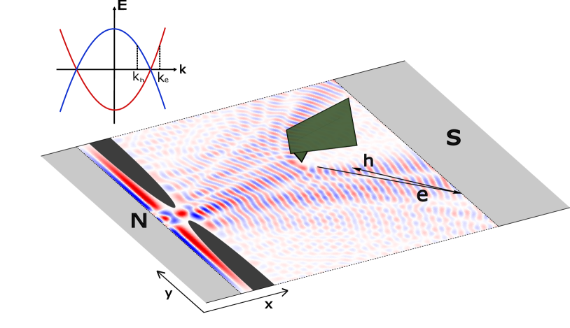
The considered system [Fig. 1] consists of a QPC embedded in the normal region of the NS junction. We consider the zero-magnetic field case, hence we use a spinless Hamiltonian written in the electron-hole basis with () z (x) Pauli matrix, meV the chemical potential and meV the superconducting gap. is the QPC potential modeled after Ref. [40] and corresponds to the potential at the 2DEG level caused by the SGM tip (located at ()) [41]. We assume that the scattering region is connected to the biased normal lead, which serves as the source of incoming electrons, and to a grounded superconducting lead, which provides the Andreev reflection. The conductance is calculated according to the Landauer-Buttiker formula [42] where is the number of electronic modes in the normal lead, electron-to-electron reflection amplitude, and electron-to-hole reflection amplitude, and the bias voltage [43]. The amplitudes are extracted from the scattering matrix of the system calculated at energy through the solution of stationary Schrödinger equation using Kwant package [44]. To account for the large size of the device in the direction parallel to the QPC gates, we apply open boundary conditions at the edges of our system in the direction. The details of the numerical simulation can be found in the Supplementary Materials [45].
The electron incident from the normal lead propagates through the QPC, whose potential is controlled by the voltage; then Andreev reflects at the superconducting contact; and finally the resulting hole is scattered back to the original normal lead. The inset of Fig. 2(a) shows a typical conductance curve versus gate voltage [46], where conductance is amplified by the Andreev reflection and quantized with plateaus in multiples of . For the following calculations we choose the value so that the resulting conductance is —at the first step—when a single branched flow is expected [21].
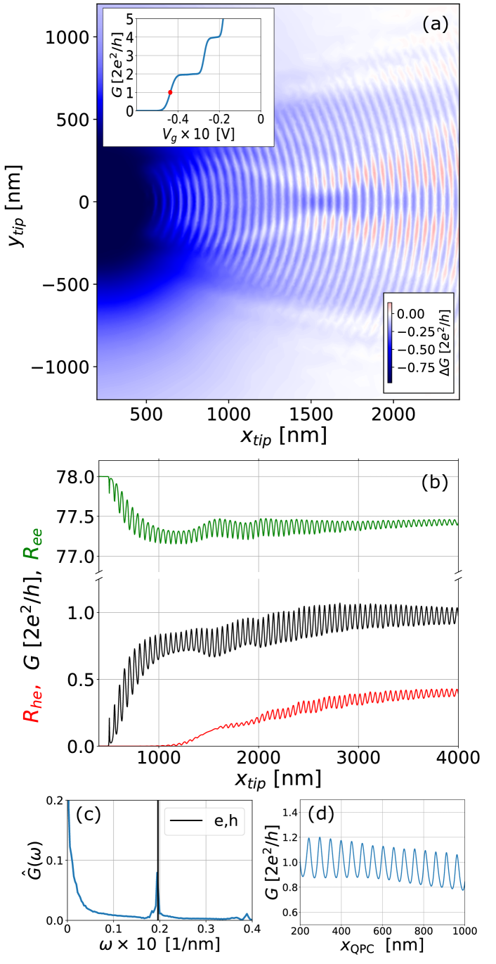
In the map of Fig. 2(a) we show the change of the conductance (difference between the conductance obtained in the presence of the tip and the conductance obtained in the absence of the tip) when the system is scanned by the SGM tip. On the map, pronounced fringes due to self-interference of the quasiparticles are present.
The conductance cross-section for the SGM coordinate set in the middle of the QPC constriction () is shown in Fig. 2(b) with the black curve. When the tip is moved away from the QPC constriction, the conductance rapidly increases as the electron flow through the QPC is unblocked and then exhibits periodic oscillations. The oscillation fringes are separated by half of the Fermi wavelength due to interference between the waves reflected by the QPC itself and those reflected back by the tip [21]. In Fig. 2(c) we show the Fourier transform of the conductance. We observe that the oscillations occur with a single period that corresponds to the Fermi wavevector of electrons and holes [47] denoted by the black vertical line in the inset with and . In a normal system such oscillations are a signature of constructive and destructive interference of the electronic wave that occurs between the QPC constriction and the SGM tip. In fact, by changing the distance between the QPC and the SGM tip, we observe conductance oscillations [Fig. 2(d)] that confirm that a similar process also takes place here. We have also checked the conductance oscillation when the superconducting interface was moved away from the QPC and SGM tip and observed their negligible amplitude (not shown). This allows us to conclude that the main path of interference is between the QPC and the SGM tip.
In Fig. 2(b) we show the transmission probabilities of the electron-electron (green curve) and electron-hole (red curve) transport process. We clearly see that most of the electrons are backscattered from the QPC giving rise to high overall values of . There is a considerable magnitude of , which means that the injected electron, after passing the QPC and scattering at the SGM tip potential, is converted into a hole at the superconducting interface that is traced back to the normal electrode. Note that in this case the interference of electrons and holes is indistinguishable, as they both have the same wavevector.
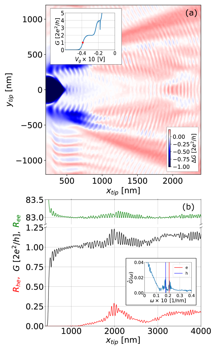
Let us now move to the non-zero voltage bias case, with . We again fix , so the conductance without the tip is in the middle of the first conductance step (see the inset of Fig. 3(a)). The corresponding map is shown in Fig. 3(a), where we observe a significant modification in the conductance pattern as compared to the case of Fig. 2(a), with three main ingredients: i) change of the pattern of oscillation fringes; ii) resonant features disturbing the previously clear single-branched flow, iii) general amplification of the conductance by the tip. As we will show in the following, they all are a signature of unequal electron and hole wave vectors.
The conductance cross-section is shown in Fig. 3(b) with the black curve. We observe that the oscillations are disturbed by a beating pattern and correspondingly in the Fourier transform (see the inset of Fig. 3(b)) we find two leading frequencies corresponding to different values of the electron and hole wavevector ( and ) obtained as with for the electron and for the hole (see the schematic dispersion relation in Fig. 1).
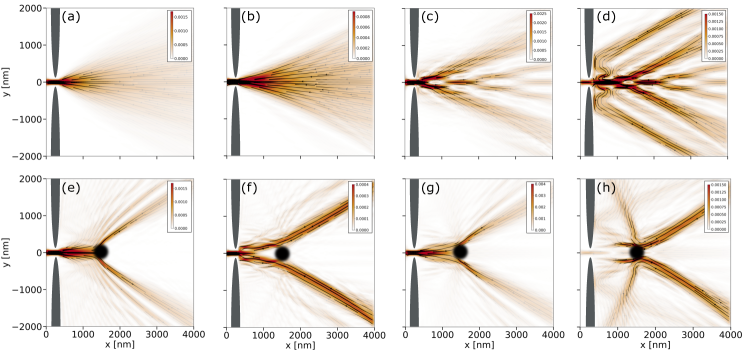
Inspecting the electron and hole contributions to the conductance shown with green and red curves, respectively, we observe a significant reduction of the amplitude compared to the zero-energy case of Fig. 2(b). This means that at the first conductance step the probability of the electron that has passed the QPC to go back to the source electrode is negligible. It is accompanied by a small amplitude. This means that the almost unity conductance is obtained mainly because of the lack of electron reflection to the left lead and not because of the Andreev reflected hole scattered back there. This initially puzzling result becomes clear when one inspects the probability current maps shown in Fig. 4. First, when considering the zero energy case we see that the electron (a) and (b) the hole currents are mostly the same, as the electron injected from the QPC is Andreev reflects and the resulting hole is back-focused into the QPC constriction. Upon introduction of the SGM tip (marked as a gray circle in the bottom row of Fig. 4) we see a deflection of the electron trajectory, but the hole does trace the electron path.
The situation is strikingly different in the non-zero energy case. First, in the absence of the tip, we clearly observe the creation of resonant features that perturb the electron [Fig. 4(c)] and hole [Fig. 4(d)] flow. The electron approaches the superconductor interface with the wavevector at an angle defined with respect to the normal to the interface. After the Andreev reflection, the hole leaving the interface has the wavevector . The momentum component along the interface is preserved and, hence, for non-zero the normal components of and are different. As a result, the hole returns from the interface following a trajectory determined by and therefore does not retrace the electron path [36] [ee the arrows in Fig. 1]. As a result the Andreev reflected hole does not focus at the QPC constriction, which results in a low value of the amplitude. In Fig. 4(d) we also observe streams of hole current that point from the QPC to the sink electrodes. The introduction of the SGM tip at those locations results in an amplification of the conductance, as the hole reflected by the tip to the QPC is now able to amplify the conductance, leading to an increase of the conductance by the tip shown in Fig. 3(a). Finally, upon introduction of the tip in Figs. 4(g) and (h) we clearly observe the effect of different incident and reflection angles, which deflects the hole current from the initial trajectory of the incident electron and, in turn, causes disturbance of the conductance pattern as seen in the map of Fig. 3(a). Similar results were obtained for the second conductance step as presented in the Supplementary Materials.
In summary, we studied theoretically the possibility of local probing of electron and hole transport in a QPC embedded in an NS junction. We proposed to use the SGM technique to observe electron and hole self-interference. We pointed out that this technique is able to unveil features of the electronic transport at non-zero bias voltage, when due to different electron and hole wavevectors the self-interference conductance oscillations exhibit beating and the Andreev-reflected hole does not retrace the electron path creating pronounced resonance patterns in the SGM probed conductance.
This work was supported by the National Science Center, Poland (NCN) agreement number UMO-2020/38/E/ST3/00418 and partially the program „Excellence initiative––research university” for the AGH University of Krakow.
References
- Andreev [1964] A. F. Andreev, Thermal conductivity of the intermediate state of superconductors, Sov. Phys. JETP. 19, (1964).
- Oreg et al. [2010] Y. Oreg, G. Refael, and F. von Oppen, Helical liquids and majorana bound states in quantum wires, Phys. Rev. Lett. 105, 177002 (2010).
- Sau et al. [2010] J. D. Sau, R. M. Lutchyn, S. Tewari, and S. Das Sarma, Generic new platform for topological quantum computation using semiconductor heterostructures, Phys. Rev. Lett. 104, 040502 (2010).
- Mourik et al. [2012] V. Mourik, K. Zuo, S. M. Frolov, S. R. Plissard, E. P. A. M. Bakkers, and L. P. Kouwenhoven, Signatures of majorana fermions in hybrid superconductor-semiconductor nanowire devices, Science 336, 1003 (2012).
- Larsen et al. [2015] T. W. Larsen, K. D. Petersson, F. Kuemmeth, T. S. Jespersen, P. Krogstrup, J. Nygård, and C. M. Marcus, Semiconductor-nanowire-based superconducting qubit, Phys. Rev. Lett. 115, 127001 (2015).
- Casparis et al. [2018] L. Casparis, M. R. Connolly, M. Kjaergaard, N. J. Pearson, A. Kringhøj, T. W. Larsen, F. Kuemmeth, T. Wang, C. Thomas, S. Gronin, G. C. Gardner, M. J. Manfra, C. M. Marcus, and K. D. Petersson, Superconducting gatemon qubit based on a proximitized two-dimensional electron gas, Nat. Nanotechnol. 13, 915 (2018).
- Larsen et al. [2020] T. W. Larsen, M. E. Gershenson, L. Casparis, A. Kringhøj, N. J. Pearson, R. P. G. McNeil, F. Kuemmeth, P. Krogstrup, K. D. Petersson, and C. M. Marcus, Parity-protected superconductor-semiconductor qubit, Phys. Rev. Lett. 125, 056801 (2020).
- Hays et al. [2021] M. Hays, V. Fatemi, D. Bouman, J. Cerrillo, S. Diamond, K. Serniak, T. Connolly, P. Krogstrup, J. Nygård, A. Levy Yeyati, A. Geresdi, and M. H. Devoret, Coherent manipulation of an andreev spin qubit, Science 373, 430 (2021).
- Davydova et al. [2022] M. Davydova, S. Prembabu, and L. Fu, Universal josephson diode effect, Sci. Adv. 8, eabo0309 (2022).
- Su et al. [2017] Z. Su, A. B. Tacla, M. Hocevar, D. Car, S. R. Plissard, E. P. A. M. Bakkers, A. J. Daley, D. Pekker, and S. M. Frolov, Andreev molecules in semiconductor nanowire double quantum dots, Nat. Commun. 8, 585 (2017).
- Wang et al. [2022] G. Wang, T. Dvir, G. P. Mazur, C.-X. Liu, N. van Loo, S. L. D. ten Haaf, A. Bordin, S. Gazibegovic, G. Badawy, E. P. A. M. Bakkers, M. Wimmer, and L. P. Kouwenhoven, Singlet and triplet cooper pair splitting in hybrid superconducting nanowires, Nature 612, 448 (2022).
- Kjaergaard et al. [2016] M. Kjaergaard, F. Nichele, H. J. Suominen, M. P. Nowak, M. Wimmer, A. R. Akhmerov, J. A. Folk, K. Flensberg, J. Shabani, C. J. Palmstrøm, and C. M. Marcus, Quantized conductance doubling and hard gap in a two-dimensional semiconductor–superconductor heterostructure, Nat. Commun. 7, 12841 (2016).
- Moehle et al. [2022] C. M. Moehle, P. K. Rout, N. A. Jainandunsing, D. Kuiri, C. T. Ke, D. Xiao, C. Thomas, M. J. Manfra, M. P. Nowak, and S. Goswami, Controlling andreev bound states with the magnetic vector potential, Nano Lett. 22, 8601 (2022).
- Moehle et al. [2021] C. M. Moehle, C. T. Ke, Q. Wang, C. Thomas, D. Xiao, S. Karwal, M. Lodari, V. van de Kerkhof, R. Termaat, G. C. Gardner, G. Scappucci, M. J. Manfra, and S. Goswami, Insbas two-dimensional electron gases as a platform for topological superconductivity, Nano Lett. 21, 9990 (2021).
- Banerjee et al. [2023] A. Banerjee, M. Geier, M. A. Rahman, D. S. Sanchez, C. Thomas, T. Wang, M. J. Manfra, K. Flensberg, and C. M. Marcus, Control of andreev bound states using superconducting phase texture, Phys. Rev. Lett. 130, 116203 (2023).
- LeRoy et al. [2002a] B. J. LeRoy, M. A. Topinka, R. M. Westervelt, K. D. Maranowski, and A. C. Gossard, Imaging electron density in a two-dimensional electron gas, Appl. Phys. Lett. 80, 4431 (2002a).
- Topinka et al. [2000] M. A. Topinka, B. J. LeRoy, S. E. J. Shaw, E. J. Heller, R. M. Westervelt, K. D. Maranowski, and A. C. Gossard, Imaging coherent electron flow from a quantum point contact, Science 289, 2323 (2000).
- Topinka et al. [2001] M. A. Topinka, B. J. LeRoy, R. M. Westervelt, S. E. J. Shaw, R. Fleischmann, E. J. Heller, K. D. Maranowski, and A. C. Gossard, Coherent branched flow in a two-dimensional electron gas, Nature 410, 183 (2001).
- LeRoy et al. [2005] B. J. LeRoy, A. C. Bleszynski, K. E. Aidala, R. M. Westervelt, A. Kalben, E. J. Heller, S. E. J. Shaw, K. D. Maranowski, and A. C. Gossard, Imaging electron interferometer, Phys. Rev. Lett. 94, 126801 (2005).
- Jura et al. [2007] M. P. Jura, M. A. Topinka, L. Urban, A. Yazdani, H. Shtrikman, L. N. Pfeiffer, K. W. West, and D. Goldhaber-Gordon, Unexpected features of branched flow through high-mobility two-dimensional electron gases, Nat. Phys. 3, 841 (2007).
- Jura et al. [2009] M. P. Jura, M. A. Topinka, M. Grobis, L. N. Pfeiffer, K. W. West, and D. Goldhaber-Gordon, Electron interferometer formed with a scanning probe tip and quantum point contact, Phys. Rev. B 80, 041303 (2009).
- Jalabert et al. [2010] R. A. Jalabert, W. Szewc, S. Tomsovic, and D. Weinmann, What is measured in the scanning gate microscopy of a quantum point contact?, Phys. Rev. Lett. 105, 166802 (2010).
- Aidala et al. [2007] K. E. Aidala, R. E. Parrott, T. Kramer, E. J. Heller, R. M. Westervelt, M. P. Hanson, and A. C. Gossard, Imaging magnetic focusing of coherent electron waves, Nat. Phys. 3, 464 (2007).
- Bhandari et al. [2016] S. Bhandari, G.-H. Lee, A. Klales, K. Watanabe, T. Taniguchi, E. Heller, P. Kim, and R. M. Westervelt, Imaging cyclotron orbits of electrons in graphene, Nano Lett. 16, 1690 (2016).
- Bhandari et al. [2020] S. Bhandari, G.-H. Lee, K. Watanabe, T. Taniguchi, P. Kim, and R. M. Westervelt, Imaging andreev reflection in graphene, Nano Lett. 20, 4890 (2020).
- Kolasiński et al. [2014] K. Kolasiński, B. Szafran, and M. P. Nowak, Imaging of double slit interference by scanning gate microscopy, Phys. Rev. B 90, 165303 (2014).
- Nowak et al. [2014] M. P. Nowak, K. Kolasiński, and B. Szafran, Signatures of spin-orbit coupling in scanning gate conductance images of electron flow from quantum point contacts, Phys. Rev. B 90, 035301 (2014).
- Kolasiński et al. [2016] K. Kolasiński, B. Szafran, B. Brun, and H. Sellier, Interference features in scanning gate conductance maps of quantum point contacts with disorder, Phys. Rev. B 94, 075301 (2016).
- Mreńca-Kolasińska et al. [2018] A. Mreńca-Kolasińska, K. Kolasiński, and B. Szafran, Imaging spin-resolved cyclotron trajectories in the insb two-dimensional electron gas, Phys. Rev. B 98, 115309 (2018).
- Mreńca-Kolasińska and Szafran [2017] A. Mreńca-Kolasińska and B. Szafran, Imaging backscattering in graphene quantum point contacts, Phys. Rev. B 96, 165310 (2017).
- Kolasiński et al. [2017] K. Kolasiński, A. Mreńca-Kolasińska, and B. Szafran, Imaging snake orbits at graphene junctions, Phys. Rev. B 95, 045304 (2017).
- Mreńca et al. [2015] A. Mreńca, K. Kolasiński, and B. Szafran, Conductance response of graphene nanoribbons and quantum point contacts in scanning gate measurements, Semicond Sci Technol 30, 085003 (2015).
- Prokop et al. [2020] M. Prokop, D. Gut, and M. P. Nowak, Scanning gate microscopy mapping of edge current and branched electron flow in a transition metal dichalcogenide nanoribbon and quantum point contact, J. Condens. Matter Phys. 32, 205302 (2020).
- Beenakker [1992] C. W. J. Beenakker, Quantum transport in semiconductor-superconductor microjunctions, Phys. Rev. B 46, 12841 (1992).
- Zhang et al. [2017] H. Zhang, Ö. Gül, S. Conesa-Boj, M. P. Nowak, M. Wimmer, K. Zuo, V. Mourik, F. K. de Vries, J. van Veen, M. W. A. de Moor, J. D. S. Bommer, D. J. van Woerkom, D. Car, S. R. Plissard, E. P. Bakkers, M. Quintero-Pérez, M. C. Cassidy, S. Koelling, S. Goswami, K. Watanabe, T. Taniguchi, and L. P. Kouwenhoven, Ballistic superconductivity in semiconductor nanowires, Nat. Commun. 8, 16025 (2017).
- Libisch et al. [2006] F. Libisch, S. Rotter, and J. Burgdörfer, Non-retracing orbits in andreev billiards, Phys. Rev. B 73, 045324 (2006).
- Kormányos et al. [2006] A. Kormányos, Z. Kaufmann, J. Cserti, and C. J. Lambert, Quantum-classical correspondence in the wave functions of andreev billiards, Phys. Rev. Lett. 96, 237002 (2006).
- Libisch et al. [2007] F. Libisch, S. Rotter, and J. Burgdörfer, Chladni figures in andreev billiards, Eur. Phys. J.: Spec. Top. 145, 245 (2007).
- Kaperek et al. [2022] K. Kaperek, S. Heun, M. Carrega, P. Wójcik, and M. P. Nowak, Theory of scanning gate microscopy imaging of the supercurrent distribution in a planar josephson junction, Phys. Rev. B 106, 035432 (2022).
- Davies et al. [1995] J. H. Davies, I. A. Larkin, and E. V. Sukhorukov, Modeling the patterned two-dimensional electron gas: Electrostatics, J. Appl. Phys. 77, 4504 (1995).
- Szafran [2011] B. Szafran, Scanning gate microscopy simulations for quantum rings: Effective potential of the tip and conductance maps, Phys. Rev. B 84, 075336 (2011).
- [42] The linear response approach, is capable of reproducing the characteristic condauctance features obtained experimentally at the finite bias [21, 48].
- Rosdahl et al. [2018] T. O. Rosdahl, A. Vuik, M. Kjaergaard, and A. R. Akhmerov, Andreev rectifier: A nonlocal conductance signature of topological phase transitions, Phys. Rev. B 97, 045421 (2018).
- Groth et al. [2014] C. W. Groth, M. Wimmer, A. R. Akhmerov, and X. Waintal, Kwant: a software package for quantum transport, New J. Phys. 16, 063065 (2014).
- [45] Supplementary Materials.
- [46] To set the working point of the QPC we close the othervise open boundary conditions at the edges opf the system along the direction.
- [47] For the discretized Hamiltonian used for the numerical calculation we use the equivalent formula for the wave-vector: with , where nm is the discretization constant.
- LeRoy et al. [2002b] B. J. LeRoy, A. C. Bleszynski, M. A. Topinka, R. M. Westervelt, S. E. J. Shaw, E. J. Heller, K. D. Maranowski, and A. C. Gossard, Imaging coherent electron flow (2002b), arXiv:cond-mat/0208194 [cond-mat.mes-hall] .