Magnetic property control of Cr2Ge2Te6 through oxidation and thickness effects
Abstract
Van der Waals (vdW) magnetic materials such as Cr2Ge2Te6 (CGT) show promise for novel memory and logic applications. This is due to their broadly tunable magnetic properties and the presence of topological magnetic features such as skyrmionic bubbles. A systematic study of thickness and oxidation effects on magnetic domain structures is important for designing devices and vdW heterostructures for practical applications. Here, we investigate thickness effects on magnetic properties, magnetic domains, and bubbles in oxidation-controlled CGT crystals. We find that CGT exposed to ambient conditions for 30 days forms an oxide layer approximately 5 nm thick. This oxidation leads to a significant increase in the oxidation state of the Cr ions, indicating a change in local magnetic properties. This is supported by real space magnetic texture imaging through Lorenz transmission electron microscopy. By comparing the thickness dependent saturation field of oxidized and pristine crystals, we find that oxidation leads to a non-magnetic surface layer with a thickness of about 10 nm, thicker than the oxide layer alone. We also find that the stripe domain width and skyrmionic bubble size are strongly affected by the crystal thickness in pristine crystals. These findings underscore the impact of thickness and surface oxidation on the properties of CGT such as saturation field and domain/skyrmionic bubble size and suggest a pathway for manipulating magnetic properties through a controlled oxidation process.
I Introduction
The discovery of long-range ferromagnetic ordering in van der Waals (vdW) materials has opened new avenues for investigating fundamental magnetism and applications within novel memory, computing, and quantum computing [1, 2, 3, 4, 5]. The tunability of vdW magnetic materials by thickness, i.e. number of atomic layers, as well as by electric fields, doping, and strain, and the presence of topological spin textures such as domain walls and skyrmions, make these materials promising for such applications [1, 2, 3]. However, an understanding of the evolution of spin textures as a function of flake thickness is highly desired for the development of future spintronic applications.
Cr2Ge2Te6 (CGT) is one such material, a vdW Heisenberg semiconducting ferromagnet with a bulk Curie temperature of about 61 K and strong perpendicular magnetic anisotropy [6, 7, 8, 9, 10]. The properties of CGT can be modified via doping [11], electric field [12, 10, 13], strain [9], and pressure [14, 15]. The latter two result from its strong magneto-elastic coupling [16]. Because CGT is centrosymmetric it lacks a Dzyaloshinskii-Moriya interaction (DMI) to stabilize Bloch or Neel-type skyrmions observed in noncentrosymmetric chiral magnets, such as B20 metals [5, 17]. Instead, it hosts topological skyrmionic Bloch-type bubbles that are stabilized through a competition between the dipolar energy and magnetocrystalline anisotropy [18, 19], making it a potential candidate for novel quantum computing methods [20].
The tunability of CGT and other vdW magnets stems from their large surface to volume ratio making the interfaces property-determining [3]. Proximitized spin-orbit coupling [21] and twisted homo- or hetero-bilayers [22, 23] are two interface effects that can tune magnetic properties of vdW magnets. A different approach may be to consider chemical effects, such as oxidation, where controlled oxidation can be used to create a chemically well-defined and non-reactive interface. CGT flakes are known to degrade in ambient air on the time scale of one hour [6, 16]. Consequently, to leverage this promising material in future applications, it is crucial to understand the effects of oxidation on its crystal and magnetic structure, and assess possibilities for magnetic property control.
Here, we prepare both pristine CGT and oxidized CGT (O-CGT) samples, and determine how crystal thickness and oxidation affect magnetic properties and magnetic domain structures. Exposure to ambient conditions leads to the formation of a 5 nm thick oxide layer. By direct imaging of magnetic domains through Lorentz transmission electron microscopy (LTEM), we find a consistently lower saturation field for O-CGT compared to CGT. These measurements suggest that up to 10 nm of the surface of the crystal, thicker than the oxide layer alone, becomes non-magnetic when it is oxidized. Compostitional analysis using electron energy loss spectroscopy (EELS) and energy dispersive x-ray (EDX) analysis shows that the oxide has a lower Te content compared to bulk CGT, and that the oxidation state of Cr increases from 3+ in the bulk to a value between 3+– 5+ in the oxide. Finally, having shown that oxidation leads to a decrease in the effective magnetic thickness, we consider how magnetic textures, which are useful for future applications, are affected by crystal thickness. We show that skyrmionic bubble sizes and stripe domain width are tuned by crystal thickness. Our results thus show that deliberate chemical modifications of the crystal surface may be another avenue towards tuning magnetic properties of vdW magnets.
II Results and Discussion
II.1 Thickness dependent saturation field of CGT and O-CGT
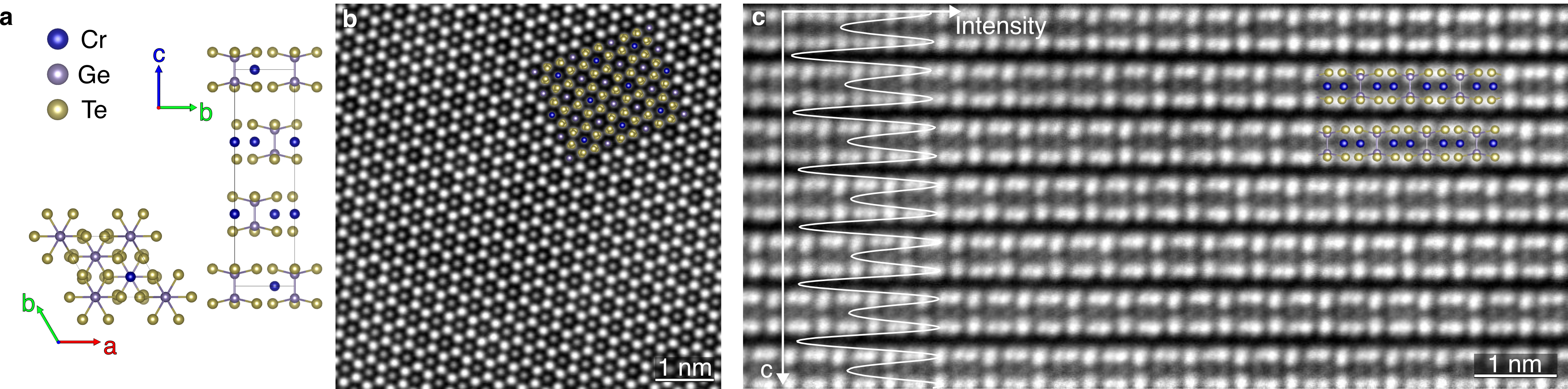
Crystal growth and sample fabrication is described in Methods. CGT crystallizes in the trigonal R space group (Fig. 1(a)) and the nominal oxidation states in bulk CGT are Cr3+, Ge3+, and Te2-. The resulting samples are single crystalline and free from observable defects and interlayer dislocations, as determined from high-angle annular dark-field scanning transmission electron microscopy (HAADF-STEM) images along the c- and a-axes (Fig. 1(b, c)), as well as TEM diffraction patterns (Fig. S1). Figure 1(c) shows the vdW layered structure with ABC stacking, consistent with previous studies [8, 18, 19]. Overlaid is an atomic model of CGT and the grey-scale intensity profile of the image averaged horizontally, from which we measure a layer thickness of 0.68 nm. Since the intensity in HAADF-STEM images is proportional to [25], being the atomic mass, Te atoms appear the brightest.
In order to control the chemical state of the surface we use one of three approaches: (1) For O-CGT we prepare samples in ambient conditions. (2) For CGT we either (a) prepare samples in an argon-filled glovebox to avoid oxygen and moisture exposure [16, 26], or (b) exfoliate CGT in ambient conditions but swiftly – within minutes – encapsulate between few-layer graphene. Details are provided in Methods and Fig. S2 shows an illustration of sample details and optical contrast measurements. Briefly, bulk CGT is exfoliated and suitable flakes are identified based on their optical contrast by first calibrating with measurements from atomic force microscopy (AFM) (Fig. S2). Optical contrast efficiently determines crystal thickness in the range 8-30 nm, but the range 5-8 nm requires AFM measurements. Pristine CGT samples prepared in the glovebox are stored within an air-sealed plastic bag, and therefore only exposed to air for some minutes before being loaded into the TEM. To form an oxide we exfoliate and transfer flakes to TEM grids, and expose to ambient conditions for periods up to 30 days before the measurements.
We first determine the saturation magnetic field in CGT and O-CGT for varying crystal thicknesses by imaging the magnetic domain structure at varying applied magnetic fields. Imaging is done using LTEM with a liquid helium cooled holder with a base temperature of 15 K [18, 27]. In the LTEM mode the magnetic field at the sample can be controlled by exciting the objective lens. The magnetic field is oriented along the z-direction, into the image plane, and the minimum achievable field in our TEM is 12 mT. Therefore, we refer to a cooling process from above the Curie temperature down to the base temperature of the sample holder at this magnetic field as “residual field cooling (RFC)” to distinguish it from a true zero-field cooling process.
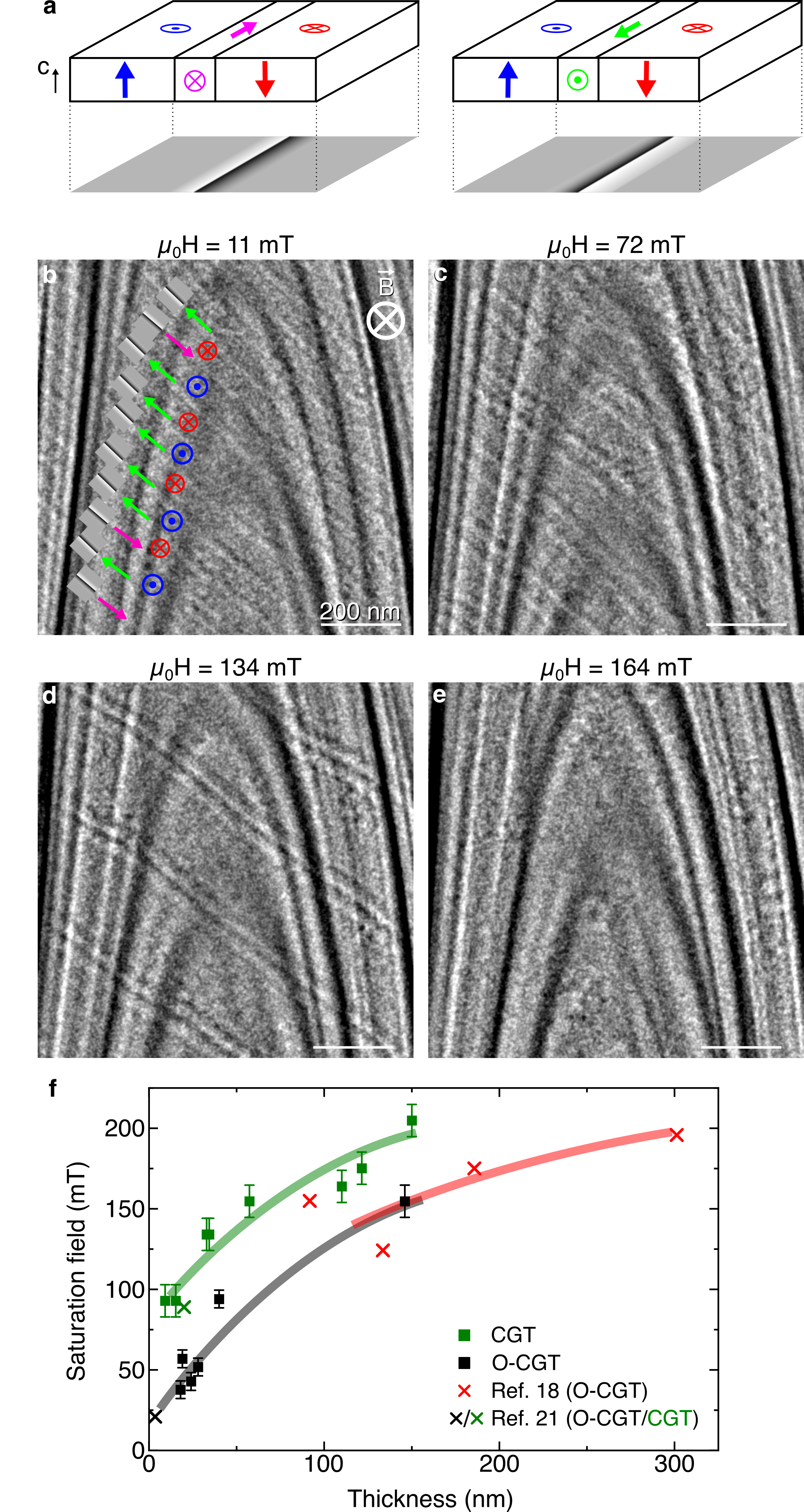
Contrast formation in Fresnel LTEM images is outlined in Fig. 2(a). The in-plane magnetization of a Bloch-type domain wall leads to dark-bright or bright-dark lines, depending on the direction of the in-plane magnetization. Hence, by considering the contrast of the magnetic features we can determine the direction of the domain walls.
Our experimental procedure to determine the saturation field is shown in Fig. 2(b-e). After RFC, stripe domains have formed, with bright-dark pairs of lines indicating the domain walls (Fig. 2(b)). The domains are magnetized along the c-directions, or in and out of the image plane, respectively, as indicated in the image. Also indicated are the direction of magnetization of the domain walls as determined by the domain wall contrast. At the residual field, the domains have approximately equal widths. Note that these images also show more slowly varying contrast such as the arch-shaped contrast. This arises from bending of the sample and is common in magnetic imaging of vdW magnets [18, 19]. This contrast is stationary when we increase the magnetic field, and therefore, of non-magnetic nature.
As the magnetic field is increased (Fig. 2(c, d)), the magnetic domains aligned with the applied magnetic field grow in width while the magnetic domains aligned in the direction opposite to the magnetic field decrease in width. Finally, we reach the saturation field when we no longer can discern any magnetic contrast in the image (Fig. 2(e)).
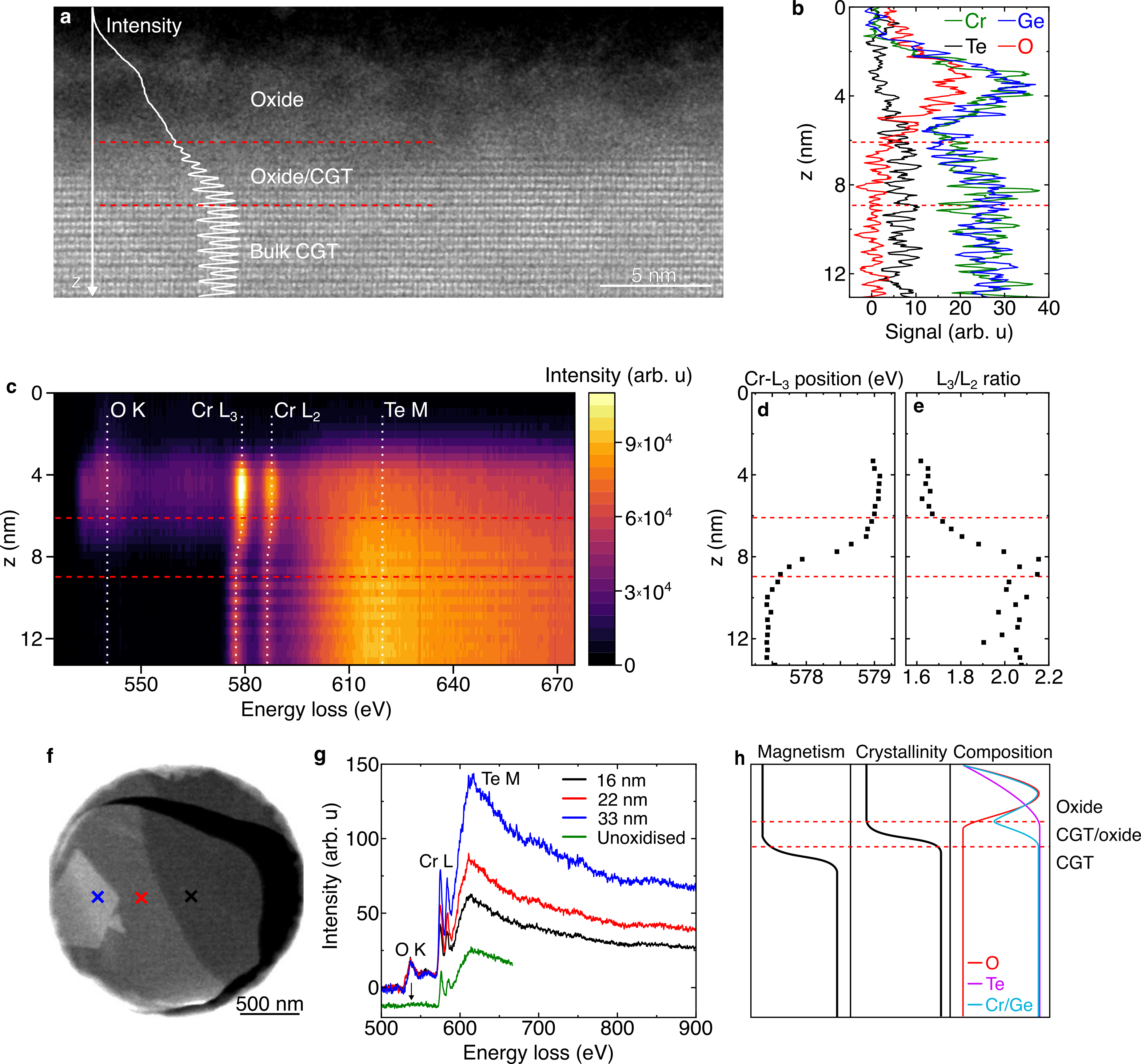
Figure 2(f) shows the saturation field plotted against crystal thickness for CGT and O-CGT. We find that the saturation field decreases with decreasing crystal thickness, and that CGT displays larger saturation fields compared to O-CGT at the same crystal thickness. This is consistent with prior studies of saturation field in CGT from which we were able to infer whether the CGT was oxidized or not [18, 24], also plotted in Fig. 2(f). We do not observe any qualitative difference in the morphology or appearance of the stripe domains between CGT and O-CGT other than the difference in the saturation field. By translating the data along the horizontal axis to make the CGT and O-CGT data coincide, we infer that the O-CGT crystals have approximately 20 nm of non-magnetic material at the top and bottom surfaces combined. This is consistent with the thinnest oxidized crystal for which we observed magnetic contrast, which had a thickness of 18 nm.
II.2 Oxide structure and composition
To further understand the effect of oxidation on the surface structure and composition of CGT crystals we combine information from several measurements (Fig. 3(a-g)). We first quantify the crystallinity using HAADF-STEM cross-sectional imaging. Figure 3(a) shows the surface of CGT viewed along the b-direction. This flake was exfoliated onto a SiO2/Si substrate and exposed to ambient conditions for 30 days before preparing the cross-sectional sample. At the top surface, we identify an amorphous oxide layer with a thickness of about 5 nm. The interface between the oxide and bulk CGT is not atomically sharp. On top of the image in Fig. 3(a) we plot the pixel intensity averaged horizontally. From the intensity profile, we estimate a transition region that is 2-3 nm thick in which some crystallinity coexists with the amorphous oxide. The lower part of the image shows bulk CGT.
Images of the bottom surface of the same sample (Fig. S3) show an oxide thickness of 2-2.5 nm. This oxide is thinner because it experiences less oxygen exposure: it is exposed to atmosphere only for the few seconds it takes to cleave the crystal using scotch tape and place it on the SiO2/Si substrate, although it is also exposed to oxygen that is trapped at the interface between CGT and SiO2 after exfoliation. The two oxide thickness measurements indicate that oxidation of CGT initially proceeds quickly but then more slowly on further air exposure as it serves as a self-passivation layer.

We next investigate the elemental composition of the oxide and interface structure with energy dispersive x-ray (EDX) analysis. Figure 3(b) shows the EDX signal across the interface, acquired from a region similar to that shown in Fig. 3(a). We find a large oxygen concentration at the oxide along with decreased Te composition compared to the bulk CGT value. There is also a decrease in the Cr and Ge signal in the mixed oxide/CGT region compared to the bulk CGT. Real space intensity maps of the Cr, Ge, Te, and O content obtained by EELS and EDX are given in Figs. S4 and S5, respectively.
We finally use electron energy loss spectroscopy (EELS) to investigate the Cr oxidation states across the interface. Figure 3(c) shows an EEL spectral map of the CGT surface shown in Fig. 3(a). We indicate the O K edge, the Cr L2 and L3 edge, and the Te M edge with dotted lines. The red horizontal dotted lines are in the same position as in Fig. 3(b) and indicate the transition between the oxide, mixed oxide/CGT, and bulk CGT. Consistent with our EDX data, we only detect an O signal at the surface of the CGT, spanning a region about 5 nm thick. We observe a 1.6-1.7 eV decrease of the Cr L2 and L3 peak positions. The L3 peak position is plotted against in Fig. 3(d) while the L3/L2 peak intensity ratio, also known as the white line intensity ratio, is plotted in Fig. 3(e). The background subtraction method is outlined in Fig. S6.
We note that the shift in peak position and L3/L2 intensity ratio takes place in the region identified in Fig. 3(a) as a mixed oxide/CGT layer. Such a shift in peak position, decrease in L3/L2 peak intensity ratio, and the presence of oxygen indicates an increase in oxidation state of the Cr [29]. The maximum possible oxidation state of Cr is 6+. However, based on the changes of these two parameters and comparing with literature values, we determine an upper bound of 5+ for the Cr oxidation state [29]. A more precise determination by comparing with published data is challenging, however [30].
Figure 3(f) shows an annular dark-field STEM image in plan-view, i.e. along the surface normal of the crystal, from an O-CGT sample with varying thickness. EEL spectra acquired from the regions indicated by the black (16 nm thick CGT), red (22 nm), and blue (33 nm) crosses are shown in Fig. 3(g). These spectra have been normalized by the oxygen K edge intensity. Since the EELS signal is proportional to the thickness of the sample, these spectra suggest a constant oxide thickness independent of CGT thickness. Also shown in Figure 3(g) is an EEL spectrum from a CGT sample prepared in a glovebox. This spectrum does not display an oxygen edge. Hence, our sample preparation protocol is able to achieve CGT samples with close to pristine surfaces due to the minimized air exposure. Samples prepared by exfoliating in ambient conditions but then rapidly encapsulating in graphene likewise do not display an oxygen peak (Fig. S7).
Figure 3(h) summarizes our structural and compositional findings. The left panel shows our conclusion from Fig. 2(f) that the surface is non-magnetic; the non-magnetic layer is thicker than the amorphous oxide layer as indicated in the middle panel. This suggests that both the oxide and the mixed oxide/CGT region are non-magnetic. This may be due to the change in oxidation state of the Cr which also changes the atomic spin moment and possibly the local magnetic interaction in the mixed oxide/CGT region and the oxide. Cr in bulk CGT has an oxidation state of 3+ and an [Ar]3d3 electronic structure with spin S=3/2, while a 4+ or 5+ oxidation state would correspond to an electronic structure of [Ar]3d2 with S=1 or [Ar]3d1 electronic structure with S=1/2, respectively.
Finally, the right panel in Fig. 3(h) summarizes our compositional findings. The loss of Te in the oxide layer may contribute to the loss of magnetism observed in the oxide. This is because the superexchange interaction responsible for ferromagnetism in CGT is mediated between nearest neighbor Cr ions through the Te cations. The loss of Te in the oxide, furthermore, is similar to other vdW transition metal chalcogenide (TMD) compounds where the chalcogen is seen to be removed in the oxidation process, such as WSe2 which forms WO3 [31] and MoS2 which forms MoO3 [32]. In such materials, oxide layer thickness and composition can be controlled using a thermal process or an oxygen plasma [33], suggesting that for CGT it may also be possible to control the oxidation process.
II.3 Thickness-dependent topological magnetic textures
Having shown how oxidation changes the effective magnetic thickness of CGT crystals we next consider how magnetic textures change with thickness. Domain walls [4] and skyrmions [5] hold potential for application in emerging spintronic memory and logic devices.
In Fig. 4 we explore the control of skyrmionic bubble size through CGT crystal thickness and magnetic field. LTEM images of CGT obtained after field cooling at a magnetic field of 52 mT results in skyrmionic bubble lattices, as previously reported for CGT [18, 19]. Increasing the magnetic field decreases the bubble size until the saturation field is reached. Figure 4(a-d) show images from a sample with a thickness of 150 nm. At 52 mT (Fig. 4(a)) the average bubble diameter is 104 nm: it decreases to 62 nm at a magnetic field of 196 mT (Fig. 4(d)), which is the last image obtained before the saturation field is reached. Figure 4(g) plots the bubble diameter against the applied magnetic field for three different samples. The size is inversely proportional to the applied magnetic field, as shown by the dashed black line in Fig. 4(g). This is as expected for skyrmions [34, 35, 36].
Materials where magnetic bubbles are stabilized by a competition between magnetic dipolar interactions and magnetocrystalline anisotropy display thickness-dependent bubble sizes [18, 37, 38]. Conversely, Bloch-type skyrmions that are stabilized by a DMI have been reported to have a size that is independent of the sample thickness [39, 40]. Figure 4(a, e, f) shows bubble lattices in several CGT crystals with different thicknesses, while Fig. 4(h) shows the bubble diameter plotted against CGT thickness, measured at a magnetic field of 52 mT. We find that the bubble diameter increases with CGT thickness (for example, diameter 90 nm at CGT thickness 82 nm; diameter 183 nm at CGT thickness 395 nm). This confirms that magnetic bubbles in CGT are stabilized by a competition between magnetic dipolar interactions and magnetocrystalline anisotropy, as expected in such a centro-symmetric material that lacks a DMI.
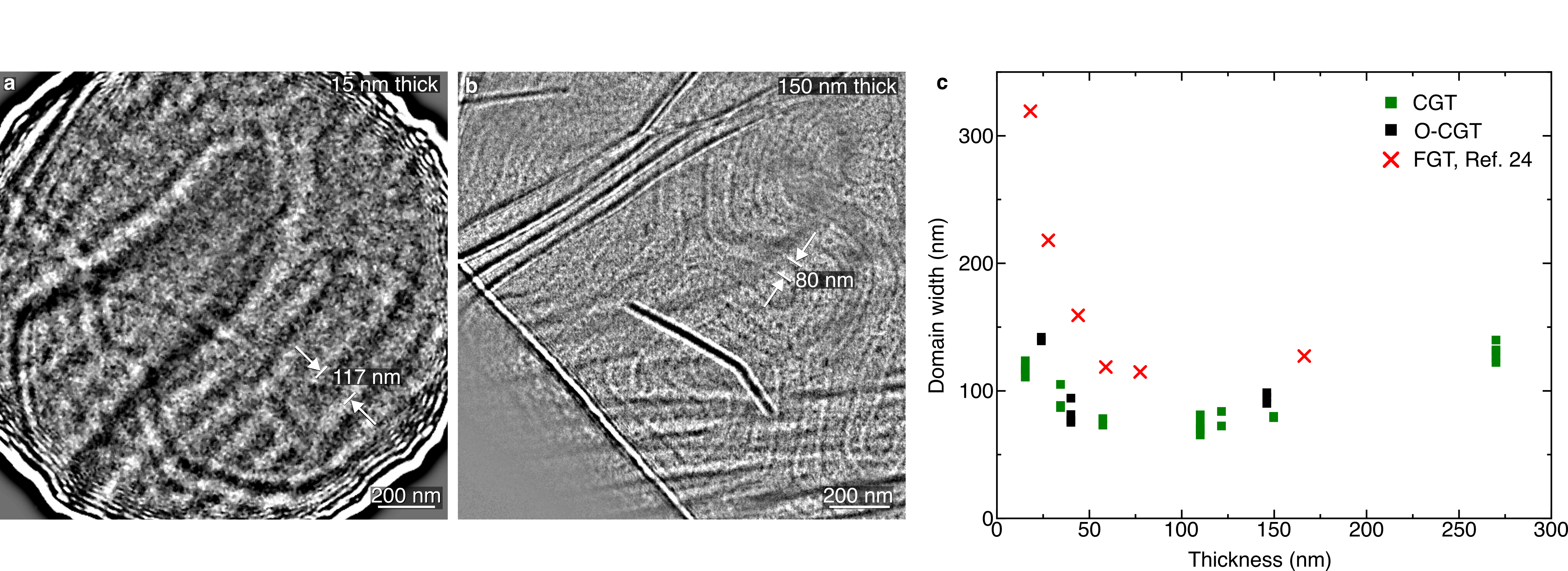
Next, considering domain energetics, Fig. 5(a, b) show LTEM images obtained at 15 K after RFC for CGT crystals that are 15 nm and 150 nm thick, respectively. The 15 nm thick crystal gives less magnetic signal and we therefore use a larger defocus value to obtain measurable magnetic contrast. Figure 5(c) shows measurements of the domain width plotted against CGT thickness. We also plot data for Fe3GeTe2 (FGT) extracted from Ref. [28]. As seen in this plot, FGT shows a similar behavior to CGT but displays larger domain width compared to CGT for the same crystal thickness. The two materials are compositionally analogous and both have been shown to oxidize in ambient conditions leading to a non-magnetic surface layer [41, 42]. This suggests that the findings here may be more widely applicable to other vdW magnets.
Kittel developed a model for the energetics of stripe domains in thick films of ferromagnetic material with out-of-plane magnetic anisotropy [43]. Kooy and Enz later extended this model to include thin membranes [44]. The domain width depends on a competition between the domain wall energy, anisotropy energy, and the demagnetizing energy (stray field energy). For very thin membranes, the domain width increases exponentially with decreasing membrane thickness. As the thickness is increased, a minimum domain width, , is reached at a thickness of , where is the vacuum permeability, is the specific domain wall energy, and is the saturation magnetization (Sec. 3.7.3 in Ref. [45]). For CGT and FGT, is reached at thickness of = 60-120 nm and =80-160 nm, respectively. By using A/m and A/m from Ref. [46], we can estimate the domain wall energy in CGT and FGT to be in the range (4-7) J/m2 and (36-71) J/m2, respectively. This implies that the domain wall energy is around one order of magnitude smaller in CGT compared to FGT. The latter value fits well with another estimate of 47 J/m2 for the domain wall energy of FGT [47]. We note that Refs. [16, 19] found sizable magnetostrictive effects in CGT, and therefore a magnetostrictive term should possibly be included in the Kooy-Enz model for completeness.
Based on the Kooy-Enz model, we would expect CGT to display behavior similar to FGT for thin layers with thickness , where the domain width increases until a critical thickness is reached and finally the sample becomes magnetized in a single domain. Measurements of ultra-thin (6 layers thick) crystals with lateral dimensions 10 m have previously been shown to have a single magnetic domain [6]. Additionally, theoretical studies have predicted that CGT hosts a thickness-dependent magnetic anisotropy which decreases for thin crystals [48, 49]. Thus, one would expect the domain wall width, , to increase for thin crystals, since , where is the exchange constant and is the anisotropy constant [45]. We measure the domain wall width for three relatively thick crystals, with thickness from 110 to 390 nm, to be in the range 6-14 nm (Fig. S8), without any clear thickness dependence. This indicates that the uniaxial anisotropy remains robust for this range of thicknesses. For thin oxidized crystals (thickness = 24 nm) we do not observe a stripe domain structure that is as well-defined as those shown in Fig. 5 (Fig. S9), which suggests a weaker magnetic anisotropy. Hence, it is important to take oxidation into account when predicting the properties of a CGT crystal. Finally, future studies should determine whether a minimum thickness exists for the presence of domain walls and skyrmionic bubbles in CGT.
III Conclusions
Our results show how oxidation yields a non-reactive and chemically well-defined surface, serving as an additional control knob for magnetic properties in CGT. This may be applicable to vdW magnets more generally, where control of the oxide growth may be achievable through thermal or plasma oxidation – as shown for TMDs [33] and with layer-by-layer control [50].
We found that exposure to ambient conditions for 30 days results in a non-magnetic surface oxide layer that is about 10 nm thick. This is consistent with the thinnest oxidized crystal in which we observed magnetic textures, with a thickness of 18 nm and shows that oxidation reduces the effective magnetic width. From EELS analysis we determined an upper bound of 5+ for the Cr oxidation state in the oxide which increased from 3+ in the bulk, indicating a change to the local magnetic properties.
We further observed a strong thickness dependence on the size of skyrmions which suggests that chemical surface control can in principle tune skyrmion sizes. Additionally, oxidation could be used for patterning, as recently demonstrated for TMDs [51]. With increasing knowledge of the electrical and magnetic properties of the surface oxide layer, and further evaluation of the degree to which its growth can be controlled in a manner analogous to the growth of oxides such as MoO3 and WO3, we speculate that surface chemical control may become a useful tool for developing electrical or magnetic applications of 2D magnets.
IV Methods
IV.1 CGT crystal growth
Bulk CGT used for the black data points in Fig. 2(f) and Fig. 4(c) was grown by the self-flux technique starting from a mixture of pure elements: Cr (99.95%, Alfa Aesar) powder, Ge (99.999%, AlfaAesar) pieces, and Te (99.9999%, Alfa Aesar) pieces. A molar ratio of 1:2:6 for Cr:Ge:Te was used. The starting materials were sealed in an evacuated quartz tube, which was heated to 1100 C over 20 hours, held at 1100 C for 3 hours, and then slowly cooled to 700 C at a rate of 1 C/hour.
Bulk CGT used for the remaining data was prepared by direct reaction from elements with an excess of Te. The high purity Te (99.9999%), Ge (99.9999%) and Cr (99.99%) were mixed in a quartz ampoule with a stochiometric ratio of 2:2:10. The 50 g of reaction mixture was sealed under high vacuum in a quartz ampoule (25x150 mm, 3 mm wall thickness) and heated in a muffle furnace for 6 hours at 1000 C with heating rate of 2 C/min. The reaction mixture was horizontally placed in furnace and mechanically shaken several times at 1000 C. The ampoule was cooled to 450 C at a rate of 6 C/hour and then left to cool freely to room temperature. The ampoule was opened inside an argon glovebox and CGT crystals with size exceeding 5x5 mm were mechanically separated from the middle of the molten ingot.
IV.2 Sample fabrication
CGT crystals were obtained by exfoliating bulk CGT using scotch tape onto substrates of 90 nm thick SiO2 on Si using 3M Magic Scotch tape. Oxidized crystals were exfoliated in ambient conditions while un-oxidized crystals were exfoliated in a glovebox. Some un-oxidized samples were prepared by exfolating the CGT in ambient conditions and immediately (within 10 minutes) assembling the CGT into a van der Waals (vdW) heterostructure with graphene encapsulation. EEL spectra of the vdW heterostructures do not display an O peak indicating the absence of any measurable oxidation (Fig. S7). This is in line with previous reports of oxidation taking place on the timescale of an hour [6].
Crystals and vdW heterostructures were then transferred to location-tagged TEM grids purchased from Norcada, Inc., Canada. The transfer was performed using wedging transfer in which a film of cellulose acetate butyrate is used as polymer handle [52, 53]. After the transfer we bake the TEM sample carriers to 80 C to improve adhesion. Finally, we dissolve the in acetone and rinse the TEM sample carriers in isopropanol.
Cross-sectional samples were prepared using a Helios Nanolab 600 DualBeam instrument (FEI). A protective layer of Pt was first deposited with the electron beam (at least 2 m thick) before the cut and the lift-out. The lamella was then attached to a half-grid and thinned down to obtain a thickness of 100 nm. The last step of the thinning process was performed with the ion beam operating at 5 V with a current of 0.15 pA to avoid damage.
IV.3 Electron microscopy
A JEOL ARM 200CF instrument equipped with cold field emission gun and double-spherical aberration-correctors at Brookhaven National Laboratory was used for LTEM and the EELS data shown in Fig. 3(g). A double-tilt liquid helium cooling holder (HCTDT 3010, Gatan, Inc.) was used for low-temperature experiments.
HAADF-STEM imaging and EELS data (for Fig. 3(a, c-e) was acquired on a probe-corrected Thermo Fisher Scientific Themis Z G3 60-200 kV S/TEM operated at 200 kV. EELS data was acquired with a Continuum EEL spectrometer and a dispersion of 0.3 eV/channel, a dwell time of 0.02 s, beam current of 50 pA, and a zero loss peak full-width half maximum of 1.9 eV. The data was denoised using principal component analysis through the implementation in Hyperspy [54].
EDX data was aqcuired with a Hitachi HF5000 environmental TEM operated at 200 kV.
IV.4 Data analysis
From each LTEM image, a 40 pixel Gaussian blurred version of the image was subtracted to remove long-range intensity variations, followed by the application of a median filter. Domain width was measured by selecting several neighboring domain walls and measuring their average distance. Magnetic bubble diameters are measuring by tracing out their perimeter, and calculating the corresponding diameter assuming a perfect circle. For both bubbles and domain walls, the position of the domain wall is determined as the transition between bright and dark contrast on the LTEM images.
IV.5 Atomic force microscopy
AFM was performed on an Asylym Research Zypher VRS AFM in tapping mode.
V Acknowledgements
This work is primarily supported through the Department of Energy BES QIS program on "Van der Waals Reprogrammable Quantum Simulator" under award number DE-SC0022277 for the work on long-range correlations, as well as partially supported by the Quantum Science Center (QSC), a National Quantum Information Research Center of the U.S. Department of Energy (DOE) on probing quantum matter. M.G. acknowledges support by the Air Force Office of Scientific Research under award number FA9550-20-1-0246. The work at the Brookhaven National Laboratory was supported by the U.S. Department of Energy (DOE), Basic Energy Sciences, Materials Science and Engineering Division under Contract No. DESC0012704. K.S.B. acknowledges the primary support of the DOE, Office of Science, Office of Basic Energy Sciences under award number DE-SC0018675. The authors acknowledge the use of the MIT.nano Characterization Facilities. The authors thank Caroline A. Ross for fruitful discussions. Figure 2(a) was created using Vesta [55]. P.N. gratefully acknowledges support from the John Simon Guggenheim Memorial Foundation (Guggenheim Fellowship) as well as support from a NSF CAREER Award under Grant No. NSF-ECCS-1944085.
References
- Gibertini et al. [2019] Gibertini, M.; Koperski, M.; Morpurgo, A. F.; Novoselov, K. S. Magnetic 2D materials and heterostructures. Nature Nanotechnology 2019, 14, 408–419.
- Burch et al. [2018] Burch, K. S.; Mandrus, D.; Park, J.-G. Magnetism in two-dimensional van der Waals materials. Nature 2018, 563, 47–52.
- Mak et al. [2019] Mak, K. F.; Shan, J.; Ralph, D. C. Probing and controlling magnetic states in 2D layered magnetic materials. Nature Reviews Physics 2019, 1, 646–661.
- Parkin et al. [2008] Parkin, S. S.; Hayashi, M.; Thomas, L. Magnetic domain-wall racetrack memory. Science 2008, 320, 190–194.
- Fert et al. [2017] Fert, A.; Reyren, N.; Cros, V. Magnetic skyrmions: advances in physics and potential applications. Nature Reviews Materials 2017, 2, 1–15.
- Gong et al. [2017] Gong, C.; Li, L.; Li, Z.; Ji, H.; Stern, A.; Xia, Y.; Cao, T.; Bao, W.; Wang, C.; Wang, Y., et al. Discovery of intrinsic ferromagnetism in two-dimensional van der Waals crystals. Nature 2017, 546, 265–269.
- Zhang et al. [2016] Zhang, X.; Zhao, Y.; Song, Q.; Jia, S.; Shi, J.; Han, W. Magnetic anisotropy of the single-crystalline ferromagnetic insulator Cr2Ge2Te6. Japanese Journal of Applied Physics 2016, 55, 033001.
- Carteaux et al. [1995] Carteaux, V.; Brunet, D.; Ouvrard, G.; Andre, G. Crystallographic, magnetic and electronic structures of a new layered ferromagnetic compound Cr2Ge2Te6. Journal of Physics: Condensed Matter 1995, 7, 69.
- Šiškins et al. [2022] Šiškins, M.; Kurdi, S.; Lee, M.; Slotboom, B. J.; Xing, W.; Mañas-Valero, S.; Coronado, E.; Jia, S.; Han, W.; van der Sar, T., et al. Nanomechanical probing and strain tuning of the Curie temperature in suspended Cr2Ge2Te6-based heterostructures. npj 2D Materials and Applications 2022, 6, 41.
- Xing et al. [2017] Xing, W.; Chen, Y.; Odenthal, P. M.; Zhang, X.; Yuan, W.; Su, T.; Song, Q.; Wang, T.; Zhong, J.; Jia, S., et al. Electric field effect in multilayer Cr2Ge2Te6: a ferromagnetic 2D material. 2D Materials 2017, 4, 024009.
- Verzhbitskiy et al. [2020] Verzhbitskiy, I. A.; Kurebayashi, H.; Cheng, H.; Zhou, J.; Khan, S.; Feng, Y. P.; Eda, G. Controlling the magnetic anisotropy in Cr2Ge2Te6 by electrostatic gating. Nature Electronics 2020, 3, 460–465.
- Zhuo et al. [2021] Zhuo, W.; Lei, B.; Wu, S.; Yu, F.; Zhu, C.; Cui, J.; Sun, Z.; Ma, D.; Shi, M.; Wang, H., et al. Manipulating ferromagnetism in few-layered Cr2Ge2Te6. Advanced Materials 2021, 33, 2008586.
- Chen et al. [2018] Chen, Y.; Xing, W.; Wang, X.; Shen, B.; Yuan, W.; Su, T.; Ma, Y.; Yao, Y.; Zhong, J.; Yun, Y., et al. Role of oxygen in ionic liquid gating on two-dimensional Cr2Ge2Te6: a non-oxide material. ACS Applied Materials & Interfaces 2018, 10, 1383–1388.
- Sun et al. [2018] Sun, Y.; Xiao, R.; Lin, G.; Zhang, R.; Ling, L.; Ma, Z.; Luo, X.; Lu, W.; Sun, Y.; Sheng, Z. Effects of hydrostatic pressure on spin-lattice coupling in two-dimensional ferromagnetic Cr2Ge2Te6. Applied Physics Letters 2018, 112, 072409.
- Lin et al. [2018] Lin, Z.; Lohmann, M.; Ali, Z. A.; Tang, C.; Li, J.; Xing, W.; Zhong, J.; Jia, S.; Han, W.; Coh, S., et al. Pressure-induced spin reorientation transition in layered ferromagnetic insulator Cr2Ge2Te6. Physical Review Materials 2018, 2, 051004.
- Tian et al. [2016] Tian, Y.; Gray, M. J.; Ji, H.; Cava, R.; Burch, K. S. Magneto-elastic coupling in a potential ferromagnetic 2D atomic crystal. 2D Materials 2016, 3, 025035.
- Nagaosa and Tokura [2013] Nagaosa, N.; Tokura, Y. Topological properties and dynamics of magnetic skyrmions. Nature nanotechnology 2013, 8, 899–911.
- Han et al. [2019] Han, M.-G.; Garlow, J. A.; Liu, Y.; Zhang, H.; Li, J.; DiMarzio, D.; Knight, M. W.; Petrovic, C.; Jariwala, D.; Zhu, Y. Topological magnetic-spin textures in two-dimensional van der Waals Cr2Ge2Te6. Nano Letters 2019, 19, 7859–7865.
- McCray et al. [2023] McCray, A. R.; Li, Y.; Qian, E.; Li, Y.; Wang, W.; Huang, Z.; Ma, X.; Liu, Y.; Chung, D. Y.; Kanatzidis, M. G., et al. Direct Observation of Magnetic Bubble Lattices and Magnetoelastic Effects in van der Waals Cr2Ge2Te6. Advanced Functional Materials 2023, 2214203.
- Psaroudaki and Panagopoulos [2021] Psaroudaki, C.; Panagopoulos, C. Skyrmion qubits: A new class of quantum logic elements based on nanoscale magnetization. Physical Review Letters 2021, 127, 067201.
- Wu et al. [2020] Wu, Y.; Zhang, S.; Zhang, J.; Wang, W.; Zhu, Y. L.; Hu, J.; Yin, G.; Wong, K.; Fang, C.; Wan, C., et al. Néel-type skyrmion in WTe2/Fe3GeTe2 van der Waals heterostructure. Nature communications 2020, 11, 3860.
- Tong et al. [2018] Tong, Q.; Liu, F.; Xiao, J.; Yao, W. Skyrmions in the Moiré of van der Waals 2D Magnets. Nano letters 2018, 18, 7194–7199.
- Hejazi et al. [2020] Hejazi, K.; Luo, Z.-X.; Balents, L. Noncollinear phases in moiré magnets. Proceedings of the National Academy of Sciences 2020, 117, 10721–10726.
- Wang et al. [2018] Wang, Z.; Zhang, T.; Ding, M.; Dong, B.; Li, Y.; Chen, M.; Li, X.; Huang, J.; Wang, H.; Zhao, X., et al. Electric-field control of magnetism in a few-layered van der Waals ferromagnetic semiconductor. Nature Nanotechnology 2018, 13, 554–559.
- Hartel et al. [1996] Hartel, P.; Rose, H.; Dinges, C. Conditions and reasons for incoherent imaging in STEM. Ultramicroscopy 1996, 63, 93–114.
- Gray et al. [2020] Gray, M. J.; Kumar, N.; O’Connor, R.; Hoek, M.; Sheridan, E.; Doyle, M. C.; Romanelli, M. L.; Osterhoudt, G. B.; Wang, Y.; Plisson, V., et al. A cleanroom in a glovebox. Review of Scientific Instruments 2020, 91.
- De Graef [2000] De Graef, M. Magnetic imaging and its applications to materials; Academic Press, 2000.
- Li et al. [2018] Li, Q.; Yang, M.; Gong, C.; Chopdekar, R. V.; N’Diaye, A. T.; Turner, J.; Chen, G.; Scholl, A.; Shafer, P.; Arenholz, E., et al. Patterning-induced ferromagnetism of Fe3GeTe2 van der Waals materials beyond room temperature. Nano Letters 2018, 18, 5974–5980.
- Daulton and Little [2006] Daulton, T. L.; Little, B. J. Determination of chromium valence over the range Cr (0)–Cr (VI) by electron energy loss spectroscopy. Ultramicroscopy 2006, 106, 561–573.
- Tan et al. [2012] Tan, H.; Verbeeck, J.; Abakumov, A.; Van Tendeloo, G. Oxidation state and chemical shift investigation in transition metal oxides by EELS. Ultramicroscopy 2012, 116, 24–33.
- Li et al. [2013] Li, H.; Lu, G.; Wang, Y.; Yin, Z.; Cong, C.; He, Q.; Wang, L.; Ding, F.; Yu, T.; Zhang, H. Mechanical exfoliation and characterization of single-and few-layer nanosheets of WSe2, TaS2, and TaSe2. Small 2013, 9, 1974–1981.
- Windom et al. [2011] Windom, B. C.; Sawyer, W.; Hahn, D. W. A Raman spectroscopic study of MoS2 and MoO3: applications to tribological systems. Tribology Letters 2011, 42, 301–310.
- Reidy et al. [2023] Reidy, K.; Mortelmans, W.; Jo, S. S.; Penn, A. N.; Foucher, A. C.; Liu, Z.; Cai, T.; Wang, B.; Ross, F. M.; Jaramillo, R. Atomic-Scale Mechanisms of MoS2 Oxidation for Kinetic Control of MoS2/MoO3 Interfaces. Nano Letters 2023,
- Wilson et al. [2014] Wilson, M. N.; Butenko, A.; Bogdanov, A.; Monchesky, T. Chiral skyrmions in cubic helimagnet films: The role of uniaxial anisotropy. Physical Review B 2014, 89, 094411.
- Romming et al. [2015] Romming, N.; Kubetzka, A.; Hanneken, C.; von Bergmann, K.; Wiesendanger, R. Field-dependent size and shape of single magnetic skyrmions. Physical Review Letters 2015, 114, 177203.
- Yang et al. [2022] Yang, S.; Ju, T.-S.; Kim, C.; Kim, H.-J.; An, K.; Moon, K.-W.; Park, S.; Hwang, C. Magnetic Field Magnitudes Needed for Skyrmion Generation in a General Perpendicularly Magnetized Film. Nano Letters 2022, 22, 8430–8436.
- Yu et al. [2014] Yu, X.; Tokunaga, Y.; Kaneko, Y.; Zhang, W.; Kimoto, K.; Matsui, Y.; Taguchi, Y.; Tokura, Y. Biskyrmion states and their current-driven motion in a layered manganite. Nature Communications 2014, 5, 3198.
- Ma et al. [2020] Ma, T.; Sharma, A. K.; Saha, R.; Srivastava, A. K.; Werner, P.; Vir, P.; Kumar, V.; Felser, C.; Parkin, S. S. Tunable magnetic antiskyrmion size and helical period from nanometers to micrometers in a D2d Heusler compound. Advanced Materials 2020, 32, 2002043.
- Yu et al. [2011] Yu, X.; Kanazawa, N.; Onose, Y.; Kimoto, K.; Zhang, W.; Ishiwata, S.; Matsui, Y.; Tokura, Y. Near room-temperature formation of a skyrmion crystal in thin-films of the helimagnet FeGe. Nature Materials 2011, 10, 106–109.
- Park et al. [2014] Park, H. S.; Yu, X.; Aizawa, S.; Tanigaki, T.; Akashi, T.; Takahashi, Y.; Matsuda, T.; Kanazawa, N.; Onose, Y.; Shindo, D., et al. Observation of the magnetic flux and three-dimensional structure of skyrmion lattices by electron holography. Nature Nanotechnology 2014, 9, 337–342.
- Li et al. [2023] Li, Y.; Hu, X.; Fereidouni, A.; Basnet, R.; Pandey, K.; Wen, J.; Liu, Y.; Zheng, H.; Churchill, H. O.; Hu, J., et al. Visualizing the Effect of Oxidation on Magnetic Domain Behavior of Nanoscale Fe3GeTe2 for Applications in Spintronics. ACS Applied Nano Materials 2023, 6, 4390–4397.
- Kim et al. [2019] Kim, D.; Park, S.; Lee, J.; Yoon, J.; Joo, S.; Kim, T.; Min, K.-j.; Park, S.-Y.; Kim, C.; Moon, K.-W., et al. Antiferromagnetic coupling of van der Waals ferromagnetic Fe3GeTe2. Nanotechnology 2019, 30, 245701.
- Kittel [1946] Kittel, C. Theory of the structure of ferromagnetic domains in films and small particles. Physical Review 1946, 70, 965.
- Kooy and Enz [1960] Kooy, C.; Enz, U. Experimental and theoretical study of domain configuration in thin layer of BaFe12O19. Philips Research Reports 1960, 15, 7–29.
- Hubert and Schäfer [2008] Hubert, A.; Schäfer, R. Magnetic domains: the analysis of magnetic microstructures; Springer Science & Business Media, 2008.
- Wu et al. [2022] Wu, Y.; Francisco, B.; Chen, Z.; Wang, W.; Zhang, Y.; Wan, C.; Han, X.; Chi, H.; Hou, Y.; Lodesani, A., et al. A van der Waals interface hosting two groups of magnetic skyrmions. Advanced Materials 2022, 34, 2110583.
- León-Brito et al. [2016] León-Brito, N.; Bauer, E. D.; Ronning, F.; Thompson, J. D.; Movshovich, R. Magnetic microstructure and magnetic properties of uniaxial itinerant ferromagnet Fe3GeTe2. Journal of Applied Physics 2016, 120.
- Fang et al. [2018] Fang, Y.; Wu, S.; Zhu, Z.-Z.; Guo, G.-Y. Large magneto-optical effects and magnetic anisotropy energy in two-dimensional Cr2Ge2Te6. Physical Review B 2018, 98, 125416.
- Song et al. [2019] Song, C.; Liu, X.; Wu, X.; Wang, J.; Pan, J.; Zhao, T.; Li, C.; Wang, J. Surface-vacancy-induced metallicity and layer-dependent magnetic anisotropy energy in Cr2Ge2Te6. Journal of Applied Physics 2019, 126.
- Zheng et al. [2018] Zheng, X.; Wei, Y.; Deng, C.; Huang, H.; Yu, Y.; Wang, G.; Peng, G.; Zhu, Z.; Zhang, Y.; Jiang, T., et al. Controlled layer-by-layer oxidation of MoTe2 via O3 exposure. ACS applied materials & interfaces 2018, 10, 30045–30050.
- Kim et al. [2023] Kim, B. S.; Sternbach, A. J.; Choi, M. S.; Sun, Z.; Ruta, F. L.; Shao, Y.; McLeod, A. S.; Xiong, L.; Dong, Y.; Chung, T. S., et al. Ambipolar charge-transfer graphene plasmonic cavities. Nature Materials 2023, 1–6.
- Thomsen et al. [2022] Thomsen, J. D.; Reidy, K.; Pham, T.; Klein, J.; Osherov, A.; Dana, R.; Ross, F. M. Suspended graphene membranes to control Au nucleation and growth. ACS Nano 2022, 16, 10364–10371.
- Thomsen et al. [2019] Thomsen, J. D.; Kling, J.; Mackenzie, D. M.; Bøggild, P.; Booth, T. J. Oxidation of suspended graphene: etch dynamics and stability beyond 1000 C. ACS Nano 2019, 13, 2281–2288.
- de la Peña et al. [2022] de la Peña, F. et al. hyperspy/hyperspy: Release v1.7.3. 2022; https://doi.org/10.5281/zenodo.7263263.
- Momma and Izumi [2011] Momma, K.; Izumi, F. VESTA 3 for three-dimensional visualization of crystal, volumetric and morphology data. Journal of Applied Crystallography 2011, 44, 1272–1276.