Integrate-and-fire circuit for converting analog signals to spikes using phase encoding
Abstract
Processing sensor data with spiking neural networks on digital neuromorphic chips requires converting continuous analog signals into spike pulses. Two strategies are promising for achieving low energy consumption and fast processing speeds in end-to-end neuromorphic applications. First, to directly encode analog signals to spikes to bypass the need for an analog-to-digital converter (ADC). Second, to use temporal encoding techniques to maximize the spike sparsity, which is a crucial parameter for fast and efficient neuromorphic processing. In this work, we propose an adaptive control of the refractory period of the leaky integrate-and-fire (LIF) neuron model for encoding continuous analog signals into a train of time-coded spikes. The LIF-based encoder generates phase-encoded spikes that are compatible with digital hardware. We implemented the neuron model on a physical circuit and tested it with different electric signals. A digital neuromorphic chip processed the generated spike trains and computed the signal’s frequency spectrum using a spiking version of the Fourier transform. We tested the prototype circuit on electric signals up to 1 KHz. Thus, we provide an end-to-end neuromorphic application that generates the frequency spectrum of an electric signal without the need for an ADC or a digital signal processing algorithm.
Keywords Spiking neural network Temporal encoding Sensor signal processing Fourier transform
1 Introduction
The human brain processes a vast amount of sensory information quickly and efficiently. This efficient and fast processing is currently unmatched by any artificial system. Hence, ongoing research aims to understand and mimic the brain’s sensory processing. An essential part of this research is encoding incoming information into spikes [1]. Coding schemes are commonly classified into rate coding and temporal coding, that assume information is stored in the rate of spike trains for a given time window or in the actual timing of the spikes, respectively. There is evidence that points toward the existence of time coding schemes in the brain [2, 3, 4], as well as for rate coding schemes [5, 6, 7]. These two paradigms can also be generalized for neuron populations, where redundant information in a group of neurons allows to reduce the inference time or the uncertainty in the signal [8]. From a conceptual point of view, rate encoding offers robustness and can be easily generalized for large populations [7]. In contrast, time coding is faster and more energy efficient, as it requires few spikes. It also explains the fast reaction times, especially for sensory pathways, that are crucial for survival [9, 10, 11]. One hypothesis of how neurons implement time coding is by carrying information in the inter-spike interval, i.e., the time between two consecutive spikes [12]. Alternatively, time coding schemes may rely on reference points in time to convey information. These references include the onset of a stimulus, spikes from other neurons, or periodic waves within the brain activity [13, 14].
One of the aims of neuromorphic research is to represent data with discrete spikes, mimicking the efficient operation of the brain. Therefore, spike encoding is a crucial step in the design of neuromorphic algorithms. When developing spiking neural networks (SNNs), the choice of the encoding scheme depends on aspects like the nature of the input data, the network architecture, or the neuron dynamics model used by the SNN. Neuromorphic computing research often focuses on high-end tasks that use processed data, e.g., classification [15], object detection [16], tracking [17], or motor control [17, 18]. These applications typically use rate encoding, as the main motivation is to validate neural models in terms of accuracy, rather than the benefits of sparsity and efficiency provided by temporal encoding schemes [19]. However, energy and time efficiency becomes more relevant for low-level neuromorphic applications that directly process sensor data. This is the case of embedded systems where the pool of energy is limited, such as automotive applications[20, 21]. There are recent examples of neuromorphic computing algorithms that deal with low-end tasks and are applied to sensor data, such as LiDAR [20], event-based cameras [22], FMCW radar [21], electrocardiogram signals [23], or microphones [24].
The interface between the sensor and the neuromorphic chip is crucial for obtaining a high energy efficiency and processing speed. When dealing with analog data, the most efficient approaches directly operate on the sensor signals by using ad-hoc circuits that encode them to spike trains. The signal-to-spike encoding mechanisms are typically application-specific, as they need to be compatible with the SNNs afterward. The idea of encoding analog signals to spikes for obtaining efficient implementations is not new. In [23] and [25], authors use temporal contrast to identify positive and negative gradients, which discriminate high and low frequencies in the analog signal. [26] introduces a VLSI circuit for implementing the interspike-interval (ISI) mechanism for encoding analog signals. The authors in [27] and [28] introduce silicon neurons for generating different spike bursting behaviours, similar to those observed in biological neurons. We refer the interested reader to [29] for getting an overview of the different analog circuits used in neuromorphic systems for real-time applications, and to [30] for a comparison of the different encoding approaches.
Some neuromorphic applications focus on generating the frequency spectrum of the incoming signal [24, 31, 32]. In these examples, an analog-to-digital converter (ADC) samples the sensor data and an SNN computes a higher-level algorithm on a digital neuromorphic chip afterward. To maximize the efficiency of these applications, the ADC should be removed by directly encoding the input signal into a spike train compatible with the digital neuromorphic chip. For the specific case of an SNN that implements the Fourier transform (FT) [32], the network needs spikes referenced to a periodic signal, as the FT algorithm works with data sampled uniformly over time. Thus, the best-suited temporal approach for these applications is phase encoding, as ISI and temporal contrast lack a signal that serves as reference over the time dimension. Additionally, the results in [30] show the benefits of phase encoding in terms of accuracy and efficiency. The benefits are more clear when comparing with rate-coded approaches, as phase coding needs down to times less spike operations for processing data [33], resulting in a lower energy footprint [19].
The work in [32] proposed an SNN that computes a mathematically equivalent version of the FT by using time encoding. The authors implemented the spiking FT (S-FT) on a digital neuromorphic chip and validated it on automotive radar data. Here, we propose adapting the leaky integrate-and-fire (LIF) neuron model for directly encoding analog signals to phase-encoded spikes, which the S-FT can use on a digital neuromorphic chip. The proposed approach leads to the implementation of an end-to-end pipeline that does not require an ADC nor a digital processing algorithm that encodes digitized signals into spikes. The proposed analog-to-spike encoder (ASE) employs phase encoding, i.e., each sample is represented by the time difference between the spike and a reference pulse. We implemented the ASE on a physical circuit and validated the system with real data by comparing the reconstructed data from the spikes with the original data. We modeled the nature of the error of the ASE for different scenarios. Moreover, we implemented the S-FT on the neuromorphic chip SpiNNaker 2 [34] and ran it with the ASE output spikes. The results show that the chip can use the spike train that results from encoding a periodic wave. To our knowledge, we provide the first end-to-end neuromorphic pipeline for generating the frequency spectrum of analog signals without employing an ADC.
2 Analog-to-spike encoder
The LIF is a century-old single-compartment neuron model that mimics the behavior of biological neurons [35]. Its simplicity makes it a widely used artificial neuron in neuromorphic engineering. The model is based on an circuit that charges with the incoming current and discharges in the absence of input, resembling the flux of ions in a biological neuron through its dendrites and the constant leak of them over time through its membrane. We can express the dynamics of the LIF as
| (1) |
where is the neuron’s membrane potential, is the resting potential, and is the input current to the neuron. The LIF model does not include the depolarization and hyperpolarization mechanisms on a biological neuron when it generates a spike. Instead, it is necessary to manually add the behavior of the spike generation and refractory period. A spike is triggered at time when crosses the threshold voltage . After the spike generation, is reset and fixed to for the neuron’s refractory period ,
| (2) | ||||
| (3) |
As artificial sensors often provide information in the form of a voltage, we modify (1) so the evolution of the membrane voltage depends on an input voltage . We also set for simplicity,
| (4) |
In the remainder of the paper, we use the time constant . By integrating (4) and setting , we obtain an encoding function that maps the input voltage to a spike time after onset,
| (5) |
Accordingly, the ideal decoding function is given by the inverse of ,
| (6) |
We implemented the LIF neuron model (4) for generating a spike train from input analog signals. We encoded the information into precise spike times using (5) and controlling the refractory period according to a reference signal.
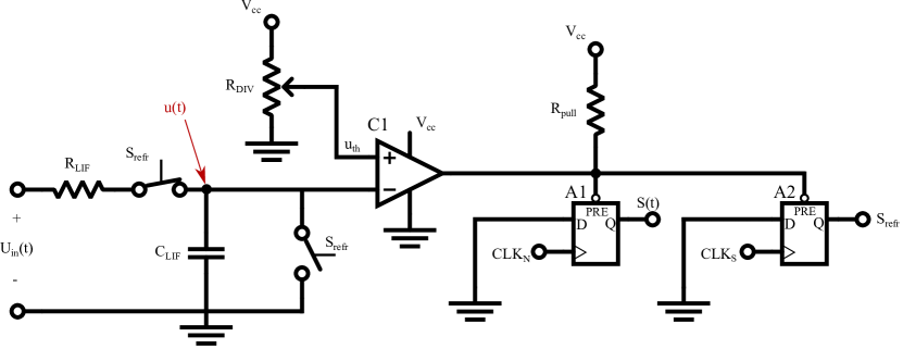
Fig. 1 shows a simplified schematic of the electric circuit we used to implement the encoder. This circuit served as a proof-of-concept for implementing an end-to-end pipeline. For implementing a high-performance circuit, we refer the interested reader to literature focused on the VLSI design of silicon neurons [29].
2.1 Encoding analog voltages with temporal spikes
By default, the LIF dynamics described in (4) generates a spike rate proportional to the input voltage . In our approach, we sample the continuous signal with a constant sampling time by generating a single spike per sample. We repeat the spike generation process for successive time windows. Thus, the spike represents the signal during the time range . This is inspired by the phase encoding technique hypothesized for the encoding of information in certain areas of the brain [14]. A binary variable forces to stay in a refractory state,
| (7) |
We achieve an adaptive refractory period, , by controlling the set and reset time of for the sample,
| (8) |
This encoding mechanism requires a periodic reference signal (see Fig. 1) that defines the sampling time and the end of the refractory period. We assume the input voltage to be constant during the sampling time of the ASE, , as the neuron dynamics is faster than the rate of change of the input signal.

The sampling time of the hardware component collecting the spikes determines the spike time resolution ,
| (9) |
2.2 Parameter tuning
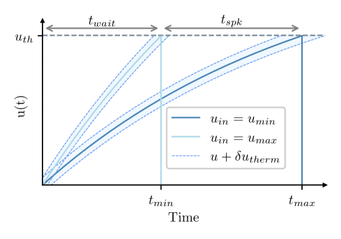
The encoder (5) has two parameters that we can tune in order to map a voltage range onto a time range , namely the time constant , and the threshold voltage . Due to the dynamics of the neuron model, we need to choose to ensure a finite time range. This leads to (see (5)) and hence introduces a waiting time before the first informative spike can arrive. We can use to reduce , but this would also lead to a smaller time range, as . To optimize the resolution in the encoding time window , we aim for a small waiting time
| (10) |
and a large spike time range
| (11) |
Hence, by maximizing the ratio
| (12) |
we can ensure to find an optimal value for (see Fig. 3). The ratio (12) is independent of . Therefore, we can only use as a scaling factor to fit the time range into the encoding window . A voltage threshold maximizes the ratio.
The overall encoding performance also depends on the decoding and the subsequent algorithms. By tuning the encoding/decoding parameters, we optimize the process. We establish three pipelines to evaluate the accuracy of the coding process. First, a coding scheme using the proposed encoding (5) and its inverse as decoding ,
| (13) |
Second, a coding scheme using the proposed encoding (5) and a linear decoding ,
| (14) |
Finally, we assess the encoder performance using a spiking algorithm that takes linearly encoded spike times as input and produces linearly encoded spike times as output. We apply the algorithm on spike times encoded as (5). To evaluate the pipeline, we compare the decoded spiking output with the output of a non-spiking version of the algorithm ,
| (15) |
For (13), the decoding does not need tuning because it is the inverse of the encoding (5). For (14) and (15), we tune the parameters of the encoding and decoding to minimize the error
| (16) |
We evaluated the encoding on the S-FT algorithm [32]. The S-FT network relies on linear coding and employs current-based LIF neurons without leak. The model assumes that the input consists in phase-encoded spikes that follow the encoding
| (17) |
and decoding
| (18) |
By calculating the error
| (19) |
with the encoding and decoding , we see that the multiplicative time constant cancels out. The error depends on the decoder’s time range , the voltage threshold of the encoder and the input voltage range , where the latter is fixed by the given setup. Due to the complexity of the relationship between the tunable parameters , and , we propose a loss function
| (20) |
that we can use to determine the optimal parameters, where defines the weight of the linear error w.r.t. the time ratio, i.e. a small puts focus on obtaining good time ratios, whereas big favors small linear errors. By setting a voltage threshold that optimizes the time ratio (12), the decoding parameters and can be determined by directly minimizing the error .
3 Validation experiments
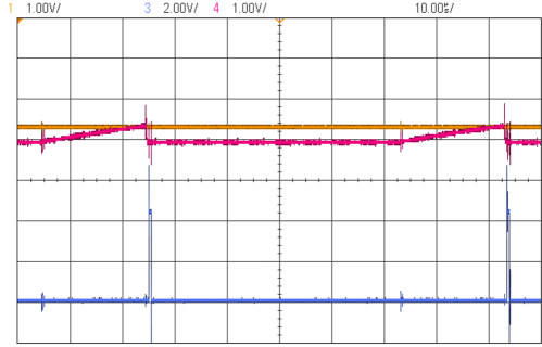
This section covers the experiment results for the proposed ASE. We implemented a prototype on an electric board with standard components. We tested the three scenarios introduced in section 2.2 with signals obtained from a function generator. We collected the spikes and generated the reset signals for the encoder with a microcontroller from the dsPIC33CK family. The minimum sampling time of the microcontroller is s, which determines the resolution of the spike times. We finally implemented the S-FT algorithm on the SpiNNaker 2 chip [34] and ran it with the spikes collected by the microcontroller.
We powered the circuit with V, and the input voltage signal was in the range of V. Fig. 4 shows a measurement of the ASE on an oscilloscope for two consecutive spikes.
3.1 Decoding of flat voltages with an ideal decoder
We tested the ASE functionality using constant voltage signals as input. We collected the generated spikes and applied the ideal decoding function (6) to the recorded spike times. In this case, the absolute error in the measurement is mainly due to the quantization error and the circuit’s thermal noise.
The spike quantization introduces a time shift to the actual spike time due to the finite resolution of the digital hardware reading the spike events. Assuming that the spike time bins are uniformly distributed with a period of , we can theoretically model this error with an average sampling error
| (21) |
On the other hand, voltage dynamics are noisy and voltage fluctuations can alter the threshold crossing time. The thermal error on the spike time highly depends on the voltage dynamics. For simplification, we model the fluctuations as a constant added to the actual membrane voltage, , and we estimate its impact on the spike time as
| (22) |
From (22), we can conclude that the thermal error on the spike times increases exponentially for small input voltages . Fig. 3 shows that thermal noise typically anticipates the spike time.
The overall measured spike time is thus obtained by combining the the quantization and the thermal noise time shifts
| (23) |
that leads to the decoding error
| (24) | ||||
| (25) |
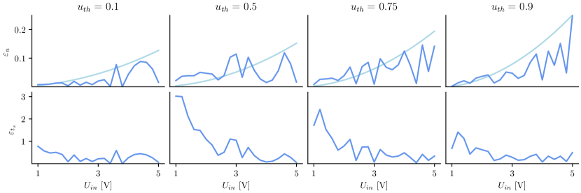
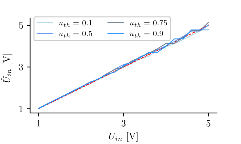
This experiment converted constant voltages in the working range V to spikes. We ran the experiment for four different setups with different threshold voltage: V (see Fig. 5).
We measured the absolute decoding error as the difference between the input voltage and the voltage that results from decoding the spike times,
| (26) |
Moreover, we also measured the error in the spike times by comparing the obtained spike times and the ideal spike times calculated with (5),
| (27) |
where we use as a normalization coefficient for making the error comparable across experiments. Fig. 5 depicts and for the ASE when using the values of from the previous experiment. We can see that the quantization error is high for high input voltages, whereas the thermal noise is low. On the other hand, low input voltages increase the probability of earlier spikes due to thermal noise, but low quantization errors in this area make spike times more precise. These errors are inherent to the used hardware and limit the accuracy of the encoding regardless of the approach followed for decoding the spikes.
We offer in Fig. 6(a) a visual comparison between the decoded voltages and the input voltages for the described experiment.
3.2 Decoding of flat voltages with a linear decoder
We tested the ASE setup from the previous section with a linear decoder (18). We used the optimization strategy introduced in section 2.2 to find the parameters from (18) that best fit the curve from the ASE. We used a differential evolution method111https://docs.scipy.org/doc/scipy/reference/generated/scipy.optimize.differential_evolution.html that minimizes (20) by adjusting and parameters that fix the decoding time limits
| (28) |
and
| (29) |
As the spike times can only be real-valued, the hard boundaries for and are . In our implementation, we chose the boundaries .
For testing the decoding, we reconstructed the original signal from the obtained spike times with the inverse of the linear encoding function (18). We evaluated the reconstruction error in terms of the root mean squared error between the original signal and the reconstructed signal
| (30) |
where is the number of samples collected during the experiment.
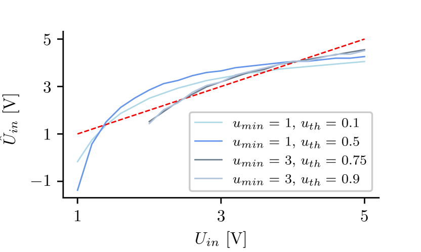
Fig. 7 depicts the decoding results for four scenarios with different and . A higher leads to a narrower input range, which directly affects the output dynamic range of the encoder, i.e., narrow voltage ranges increase the waiting time until a spike can take place. On the other hand, the mapping of the ASE has a smaller curvature, which diminishes the error when using a linear decoder (18). These two effects are counterbalanced with the threshold voltage, as a higher leads to a higher dynamic range, and lower values reduce the decoding error.
After validating the optimizer on the theoretical scenarios, we applied the fitted curves to data from the experiments with real data in section 3.1. Fig. 6(b) shows the obtained decoded voltages to four scenarios, with V, and V. Results show that narrowing down the input voltage range is the best way of improving the decoding error at the expense of reducing the output dynamic range. The results for V also show that a higher leads to a larger curvature and thus increases the output dynamic range. This effect is reduced for the results for V because the change in the ratio is smaller for the shown experiments. Increasing to values closer to would bring more significant improvements to the output dynamic range.
3.3 Computing the S-FT with the ASE output
We tested the performance of the ASE for an end-to-end pipeline that computes the frequency spectrum of the input signal. For the input, we used a function generator that creates signals consisting of one sinusoidal component. These signals can be defined as
| (31) |
where , , and are the amplitude, frequency, and offset of the sinusoidal wave, respectively. We connected the function generator to the ASE, generating one spike per sampling period . Finally, we ran the S-FT algorithm on a SpiNNaker 2 board with the spikes generated from the ASE.
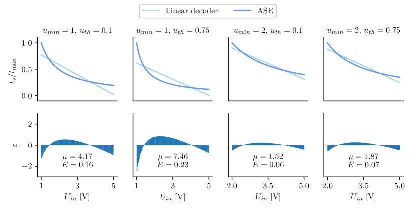
We tested the implementation for frequencies in the range . Same as for the experiment in Section 3.2, we created experiments with two different setups for the input voltage range. Namely, a working range of V, and a working range of V, i.e., we used the parameters and , and and , respectively. We fixed V and ms, and the resolution per spike to time steps. These parameters lead to maximum spiking times of and s for the wide and narrow input voltage ranges, respectively.
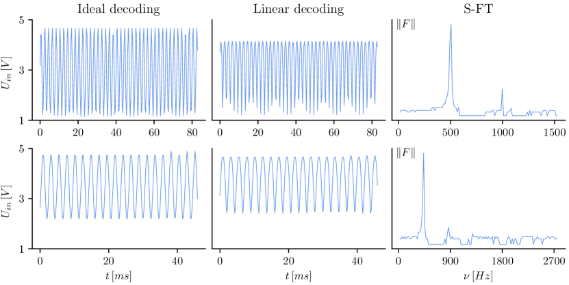
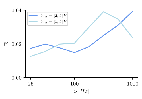
In Fig. 8, we compare the result of decoding the spikes of the ASE using an ideal decoder and a linear decoder for a wide and narrow input voltage range, respectively. We also show on the right the result of the S-FT for both input ranges. The results correspond to a setup with a frequency of Hz. We repeated this experiment for frequencies Hz and calculated the root mean squared error (30) between the obtained frequency spectrum and an FFT computed with a synthetic sine wave sampled with an ideal ADC. We show the error for the different frequencies in Fig. 9.
4 Discussion
We modelled the expected output of the proposed ASE from a theoretical perspective and validated its behaviour with experiments on analog signals. In Section 3.1 we modelled the error in the spike encoding as a combination of a quantization error and the thermal error present in analog circuits. We proved that the quantization error grows exponentially with the value of the input voltage, and the experiments show evidence that this is the dominating error in the output spikes. The experiment in Section 3.1 tested this hypothesis by converting input voltage signals in the range V to spikes and decoding them back into voltages. We show the measured error in the decoding on the top row of Fig. 5 and compare it with the quantization error equivalent to half of a time step in the spike times, i.e., the difference between the input voltage and the voltage that the corresponding spike actually represents. We also show the errors in the spike times on the bottom row of Fig. 5. The results indicate that errors in the spike times, mostly due to thermal error, are larger for low input voltages. However, these errors do not have a big effect on the decoding error, as it is mostly dominated by the quantization error. Finally, Fig. 6(a) shows the relationship between input and decoded voltages for the considered voltage range and for four different values of . We observe that the decoding stays close to the target value, and that errors are more significant towards high values of .
The experiment in in Section 3.2 fit a linear decoder to the mapping curve of different setups of the ASE. This step is necessary before implementing the ASE together with the S-FT, as the latter assumes phase-encoded input spike times. We fit a linear decoder for four different ASE setups, where we vary and , and we evaluated the result in terms of the decoding error and the dynamic output range . We can observe that both parameters have a big influence on both indicators. Large parameter values lead to small errors and narrow dynamic ranges. In general, the actual choice of parameters will depend on the requirements and limitations of the application. If the SNN that processes the spikes is not limited to a linear encoding function the design should aim to maximize , as the decoding error will stay close to zero (see top and bottom plots in Fig. 6).
The experiment described in Section 3.3 tested the ASE together with a digital neuromorphic chip for computing the frequency spectrum of the input analog signal. As we aimed to minimize the error in the generated spectrum, we chose V. We run experiments for input signal frequencies up to kHz and and V, and fit a linear decoding function for each setup. Fig. 8 depicts the results for Hz. The non-linear behaviour of the ASE (5) can be approximated by a hyperbolic function assuming small ratios , which leads to a compression of the data for low values of , and an expansion of the encoding range for high values of . This translates into the appearance of harmonics in the resulting S-FT, which is specially noticeable for larger input dynamic ranges (see top right plot of Fig. 8). We also plot the total error of the generated frequency spectrum with that of an FFT applied on a synthetic signal sampled with an ideal ADC, i.e., simulated on a PC without any added noise. The error stays relatively low, and its mostly due to the usage of a decoding function different to the encoding one. We observe bigger errors for higher frequencies and higher input voltage ranges. For , this trend stops at Hz , as after this frequency the second harmonic of the main signal is out of the range of the generated FT. This source of noise is easy to model, and this error could be mitigated with a post-processing algorithm.
5 Conclusion
We proposed adapting the widely used LIF neuron model for mapping analog signals into spike trains using phase encoding. By using an adaptive refractory period, the output spike train keeps a notion of the sampling rate, which is a fundamental requirement for applying FT-based frequency spectrum analysis techniques.
We constructed a circuit prototype and ran it on simple periodic waves to validate the model. Our experiments show that the proposed approach can encode voltages with high accuracy. Moreover, we used the output of the ASE for running a spike-based FT on the digital neuromorphic chip SpiNNaker 2. This implementation is more efficient and simpler than previous approaches, as it does not require an ADC between the sensor and the digital chip.
Future work shall focus on generating a comprehensive benchmark of the ASE by creating a VLSI version of the circuit and assessing its performance with complex data obtained from actual sensors. Those benchmarks shall include critical parameters like energy efficiency and the robustness to the noise of the ASE, and compare them with the equivalent parameters of ADCs.
Acknowledgments
The authors would like to thank Alexander Lenz and Susanne Junghans for their expertise and input, which was very valuable for implementing and testing the designed circuit. The authors would also like to thank the Technical University of Dresden for granting them access to the SpiNNaker 2 chip and its associated resources.
This research has been funded by the Federal Ministry of Education and Research of Germany in the framework of the KI-ASIC project, with identification number 16ES0995.
References
- [1] R. Brette, “Philosophy of the spike: rate-based vs. spike-based theories of the brain,” Frontiers in systems neuroscience, p. 151, 2015.
- [2] W. Bair and C. Koch, “Temporal precision of spike trains in extrastriate cortex of the behaving macaque monkey,” Neural Computation, vol. 8, no. 6, p. 1185–1202, 1996.
- [3] D. S. Reich, F. Mechler, K. P. Purpura, and J. D. Victor, “Interspike intervals, receptive fields, and information encoding in primary visual cortex,” The Journal of Neuroscience, vol. 20, no. 5, p. 1964–1974, 2000.
- [4] R. Brasselet, S. Panzeri, N. K. Logothetis, and C. Kayser, “Neurons with stereotyped and rapid responses provide a reference frame for relative temporal coding in primate auditory cortex,” The Journal of Neuroscience, vol. 32, no. 9, p. 2998–3008, 2012.
- [5] D. H. Hubel and T. N. Wiesel, “Receptive fields and functional architecture of monkey striate cortex,” The Journal of Physiology, vol. 195, 1968.
- [6] D. J. Heeger, “Normalization of cell responses in cat striate cortex,” Visual Neuroscience, vol. 9, no. 2, p. 181–197, 1992.
- [7] M. London, A. Roth, L. Beeren, M. Häusser, and P. E. Latham, “Sensitivity to perturbations in vivo implies high noise and suggests rate coding in cortex,” Nature, vol. 466, no. 7302, p. 123–127, 2010.
- [8] A. Pouget, P. Dayan, and R. S. Zemel, “Inference and computation with population codes,” Annual Review of Neuroscience, vol. 26, no. 1, p. 381–410, 2003.
- [9] P. Heil, “First-spike latency of auditory neurons revisited,” Current Opinion in Neurobiology, vol. 14, no. 4, pp. 461–467, 2004.
- [10] T. Gollisch, “Throwing a glance at the neural code: Rapid information transmission in the visual system,” HFSP Journal, vol. 3, no. 1, p. 36–46, 2009.
- [11] J. G. Martin, C. E. Davis, M. Riesenhuber, and S. J. Thorpe, “Zapping 500 faces in less than 100 seconds: Evidence for extremely fast and sustained continuous visual search,” Scientific Reports, vol. 8, no. 1, 2018.
- [12] A.-M. M. Oswald, B. Doiron, and L. Maler, “Interval coding. i. burst interspike intervals as indicators of stimulus intensity,” Journal of neurophysiology, vol. 97, no. 4, pp. 2731–2743, 2007.
- [13] G. Buzsáki and E. I. Moser, “Memory, navigation and theta rhythm in the hippocampal-entorhinal system,” Nature Neuroscience, vol. 16, no. 2, p. 130–138, 2013.
- [14] N. Hakim and E. K. Vogel, “Phase-coding memories in mind,” PLOS Biology, vol. 16, no. 8, p. e3000012, 2018.
- [15] B. Rueckauer, I.-A. Lungu, Y. Hu, M. Pfeiffer, and S.-C. Liu, “Conversion of continuous-valued deep networks to efficient event-driven networks for image classification,” Frontiers in neuroscience, vol. 11, p. 682, 2017.
- [16] J. López-Randulfe, T. Duswald, Z. Bing, and A. Knoll, “Spiking neural network for fourier transform and object detection for automotive radar,” Frontiers in Neurorobotics, vol. 15, p. 688344, 2021.
- [17] Z. Cao, L. Cheng, C. Zhou, N. Gu, X. Wang, and M. Tan, “Spiking neural network-based target tracking control for autonomous mobile robots,” Neural Computing and Applications, vol. 26, pp. 1839–1847, 2015.
- [18] R. Stagsted, A. Vitale, J. Binz, L. Bonde Larsen, Y. Sandamirskaya, et al., “Towards neuromorphic control: A spiking neural network based pid controller for uav,” in Robotics: Science and Systems 2020, RSS, 2020.
- [19] S. Davidson and S. B. Furber, “Comparison of artificial and spiking neural networks on digital hardware,” Frontiers in Neuroscience, vol. 15, p. 651141, 2021.
- [20] S. Zhou, Y. Chen, X. Li, and A. Sanyal, “Deep scnn-based real-time object detection for self-driving vehicles using lidar temporal data,” IEEE Access, vol. 8, pp. 76903–76912, 2020.
- [21] B. Vogginger, F. Kreutz, J. López-Randulfe, C. Liu, R. Dietrich, H. A. Gonzalez, D. Scholz, N. Reeb, D. Auge, J. Hille, et al., “Automotive radar processing with spiking neural networks: Concepts and challenges,” Frontiers in Neuroscience, p. 414, 2022.
- [22] U. Rançon, J. Cuadrado-Anibarro, B. R. Cottereau, and T. Masquelier, “Stereospike: Depth learning with a spiking neural network,” IEEE Access, vol. 10, pp. 127428–127439, 2022.
- [23] S. Gerber, M. Steiner, G. Indiveri, E. Donati, et al., “Neuromorphic implementation of ecg anomaly detection using delay chains,” in 2022 IEEE Biomedical Circuits and Systems Conference (BioCAS), pp. 369–373, IEEE, 2022.
- [24] D. Auge, J. Hille, F. Kreutz, E. Mueller, and A. Knoll, “End-to-end spiking neural network for speech recognition using resonating input neurons,” in Artificial Neural Networks and Machine Learning–ICANN 2021: 30th International Conference on Artificial Neural Networks, Bratislava, Slovakia, September 14–17, 2021, Proceedings, Part V 30, pp. 245–256, Springer, 2021.
- [25] K. Burelo, G. Ramantani, G. Indiveri, and J. Sarnthein, “A neuromorphic spiking neural network detects epileptic high frequency oscillations in the scalp eeg,” Scientific Reports, vol. 12, no. 1, p. 1798, 2022.
- [26] C. Zhao, Y. Yi, J. Li, X. Fu, and L. Liu, “Interspike-interval-based analog spike-time-dependent encoder for neuromorphic processors,” IEEE Transactions on Very Large Scale Integration (VLSI) Systems, vol. 25, no. 8, pp. 2193–2205, 2017.
- [27] P. Livi and G. Indiveri, “A current-mode conductance-based silicon neuron for address-event neuromorphic systems,” in 2009 IEEE international symposium on circuits and systems, pp. 2898–2901, IEEE, 2009.
- [28] J. H. Wijekoon and P. Dudek, “Compact silicon neuron circuit with spiking and bursting behaviour,” Neural Networks, vol. 21, no. 2-3, pp. 524–534, 2008.
- [29] E. Chicca, F. Stefanini, C. Bartolozzi, and G. Indiveri, “Neuromorphic electronic circuits for building autonomous cognitive systems,” Proceedings of the IEEE, vol. 102, no. 9, pp. 1367–1388, 2014.
- [30] E. Forno, V. Fra, R. Pignari, E. Macii, and G. Urgese, “Spike encoding techniques for iot time-varying signals benchmarked on a neuromorphic classification task,” Frontiers in Neuroscience, vol. 16, p. 999029, 2022.
- [31] G. Orchard, E. P. Frady, D. B. D. Rubin, S. Sanborn, S. B. Shrestha, F. T. Sommer, and M. Davies, “Efficient neuromorphic signal processing with loihi 2,” in 2021 IEEE Workshop on Signal Processing Systems (SiPS), pp. 254–259, IEEE, 2021.
- [32] J. López-Randulfe, N. Reeb, N. Karimi, C. Liu, H. A. Gonzalez, R. Dietrich, B. Vogginger, C. Mayr, and A. Knoll, “Time-coded spiking fourier transform in neuromorphic hardware,” IEEE Transactions on Computers, vol. 71, no. 11, pp. 2792–2802, 2022.
- [33] W. Guo, M. E. Fouda, A. M. Eltawil, and K. N. Salama, “Neural coding in spiking neural networks: A comparative study for robust neuromorphic systems,” Frontiers in Neuroscience, vol. 15, p. 638474, 2021.
- [34] S. Höppner, Y. Yan, A. Dixius, S. Scholze, J. Partzsch, M. Stolba, F. Kelber, B. Vogginger, F. Neumärker, G. Ellguth, et al., “The spinnaker 2 processing element architecture for hybrid digital neuromorphic computing,” arXiv preprint arXiv:2103.08392, 2021.
- [35] L. F. Abbott, “Lapicque’s introduction of the integrate-and-fire model neuron (1907),” Brain research bulletin, vol. 50, no. 5-6, pp. 303–304, 1999.