Aix Marseille Univ, CNRS, Centrale Marseille, Institut Fresnel, Institut Marseille Imaging, AMUTech, 13013 Marseille, France]Aix Marseille Univ, CNRS, Centrale Marseille, Institut Fresnel, Institut Marseille Imaging, AMUTech, 13013 Marseille, France \alsoaffiliation[Multiwave Technologies AG, 3 Chemin du Pre Fleuri, Geneva, 1228, Switzerland] Multiwave Technologies AG, 3 Chemin du Pre Fleuri, Geneva, 1228, Switzerland \alsoaffiliation[Institute of Photonics and Optical Science (IPOS), School of Physics, The University of Sydney, Sydney, NSW 2006, Australia] Institute of Photonics and Optical Science (IPOS), School of Physics, The University of Sydney, Sydney, NSW 2006, Australia Institute of Photonics and Optical Science (IPOS), School of Physics, The University of Sydney, Sydney, NSW 2006, Australia] Institute of Photonics and Optical Science (IPOS), School of Physics, The University of Sydney, Sydney, NSW 2006, Australia \alsoaffiliation[The University of Sydney Nano Institute, The University of Sydney, Sydney, NSW 2006, Australia] The University of Sydney Nano Institute, The University of Sydney, Sydney, NSW 2006, Australia Institute of Photonics and Optical Science (IPOS), School of Physics, The University of Sydney, Sydney, NSW 2006, Australia] Institute of Photonics and Optical Science (IPOS), School of Physics, The University of Sydney, Sydney, NSW 2006, Australia \alsoaffiliation[The University of Sydney Nano Institute, The University of Sydney, Sydney, NSW 2006, Australia] The University of Sydney Nano Institute, The University of Sydney, Sydney, NSW 2006, Australia Aix Marseille Univ, CNRS, Centrale Marseille, Institut Fresnel, Institut Marseille Imaging, AMUTech, 13013 Marseille, France]Aix Marseille Univ, CNRS, Centrale Marseille, Institut Fresnel, Institut Marseille Imaging, AMUTech, 13013 Marseille, France Aix Marseille Univ, CNRS, Centrale Marseille, Institut Fresnel, Institut Marseille Imaging, AMUTech, 13013 Marseille, France]Aix Marseille Univ, CNRS, Centrale Marseille, Institut Fresnel, Institut Marseille Imaging, AMUTech, 13013 Marseille, France Institute of Photonics and Optical Science (IPOS), School of Physics, The University of Sydney, Sydney, NSW 2006, Australia] Institute of Photonics and Optical Science (IPOS), School of Physics, The University of Sydney, Sydney, NSW 2006, Australia \alsoaffiliation[The University of Sydney Nano Institute, The University of Sydney, Sydney, NSW 2006, Australia] The University of Sydney Nano Institute, The University of Sydney, Sydney, NSW 2006, Australia Institute of Photonics and Optical Science (IPOS), School of Physics, The University of Sydney, Sydney, NSW 2006, Australia] Institute of Photonics and Optical Science (IPOS), School of Physics, The University of Sydney, Sydney, NSW 2006, Australia \alsoaffiliation[The University of Sydney Nano Institute, The University of Sydney, Sydney, NSW 2006, Australia] The University of Sydney Nano Institute, The University of Sydney, Sydney, NSW 2006, Australia
Broadband terahertz near-field excitation and detection of silicon photonic crystal modes
Abstract
Chip-based terahertz (THz) devices are emerging as versatile tools for manipulating mm-wave frequencies in the context of integrated high-speed communication technologies for potential sixth-generation (6G) wireless applications. The characterization of THz devices is typically performed using far-field techniques that provide limited information about the underlying physical mechanisms producing them. As the library of chip-based functionalities expands, e.g., for tailoring the emission and directional propagation properties of THz antennas and waveguides, novel characterization techniques will likely be beneficial for observing subtle effects that are sensitive to a device’s structural parameters. Here we present near-field measurements showing the emission properties of a broadband THz emitter placed in the vicinity of a photonic crystal (PHC) slab. These experiments reveal long-predicted emission properties, but which to our knowledge have yet to be experimentally observed at THz frequencies. We demonstrate three distinct effects between 0.3-0.5 THz: (i) field suppression at frequencies corresponding to quasi-TE bandgaps (ii) a frequency-dependent directed emission along two distinct pathways for two neighboring frequencies, resulting in a local field concentration; (iii) a re-direction of the emission, achieved by rotating the PHC with respect to the dipole orientation. Simulations reveal that the observed behavior can be predicted from the underlying band structure. Our results highlight the opportunities that PHCs can potentially provide for alignment-free, chip-based 6G technologies. Our experimental technique extends the applicability realms of THz spectroscopy and will find use for characterizing the THz modes supported by true samples, whose inherent imperfections cannot realistically be accounted for by simulations, particularly in highly dispersive frequency bands.
1 Introduction
The terahertz (THz) frequency range 1, which spans 0.1-10 THz and corresponds to wavelengths between 3 mm–30 m, holds potential for a wide range of applications including bio-sensing 2, 3, non-destructive imaging 4, spectroscopy 5, space communication 6, and telecommunications 7. Recent years, in particular, have witnessed a surge in interest in terahertz technologies that may serve the imminent rollout of 6G telecommunication networks with terabits/s data rates 8, which will be essential for providing a reliable communication backbone for several emerging technologies and systems 9, such as interconnected vehicles, augmented and virtual reality, and artificial intelligence. As a result, much effort has been directed towards the development of increasingly efficient, compact, and reliable terahertz interconnect solutions 10, 11.
In the context of free-space communication, terahertz radiation uniquely provides a bridge between optics and electronics 12, sharing the advantages of both IR waves (high directivity, large bandwidth) and microwaves (reduced diffraction). However, the strong dependence on atmospheric conditions 13, the large absorption of water and vapour 14, signal interference 15, the loss of the long-range free space path 16, and the need for precise alignment between the source and receiver 17, limit the practicality of THz wireless links. To address this, recent years have been marked by the emergence of waveguide-based (sometimes referred to as wired) terahertz communication platforms 18, which have the potential to overcome some of the above challenges. Examples of short-haul wired terahertz links 19 ( cm) include photonic crystal 20 (PC), topological 21, and suspended 22 waveguides; medium-haul links () are typically achieved with THz fibers 23, 24.Longer-haul links are less common, due to the intrinsic large losses of solid materials relative to other frequency bands, and due to large bend losses in the case of large-area hollow core waveguides 25.
The emergence of wired devices has, in turn, been accompanied by a wide range of passive components that need to seamlessly interface between multiple functional devices, including, for example, directional couplers and splitters 26, and frequency multiplexers 27, 28, which ideally occupy the smallest possible footprint, and are thus best suited for integration with short-haul devices. The most popular material for short-haul applications is float zone silicon 29, because it exhibits extremely low loss in the THz range, strong confinement (refractive index: 3.42), and can be fabricated using established deep-etching fabrication processes 30. Most existing designs for beam steering demand appropriately engineered and at times rather sophisticated waveguide arrangements (e.g., using leaky 31 and coupled metallic wire 28 arrangement, or appropriate defects within photonic crystals 27 and metasurfaces 32, 33.)
On the other hand, it is well known that bulk photonic crystals (PCs) 34 and metasurfaces 35 exhibit a rich underlying bandstructure which, even without defects, can enhance or suppress emission of nearby sources 36, e.g. dipole antennae 37 (in the microwave regime) and quantum dots 38 (in the near-IR), or provide diffractionless propagation 39 or long-range supercollimation 40, 41, enabling alignment-free self-guiding 42, 43 at specific frequencies. Such effects rely on a tailored local density of states via a flattening of the isofrequency contours at specific frequencies 44, 45, 46, 47. In such regions, self-guiding 43 or directed emission 42, 34 are supported, depending on whether the input is a collimated beam or a point dipole. Although these effects have been known for more than 20 years, self-collimation effects after far-field coupling have, to the best of our knowledge, only been measured directly at microwave and near-IR frequencies 46, 47, 48, 49, 41, 50, 51, 52, 53, 54. Directed emission from a dipole antenna directly placed the near field has been observed in the microwave range 55, 56, 49, 57, with a maximum reported frequency of 40 GHz in photonic crystals 46, due to the experimental challenges associated with other spectral regions. At higher frequencies, most experiments either excite or collect radiation from an external source far from the sample, which provides a lot of information about the overall transmission and reflection properties into the far field, but no information on the field profiles within the sample itself, and any subtle physics that emerges therein.
Here we present experiments revealing exquisitely controlled emission of a broadband terahertz dipole emitter and detector located in close proximity to a terahertz photonic crystal formed by a silicon slab containing periodic sub-wavelength holes. We perform near-field emission and detection experiments showing electric field suppression when the dipole frequency lies within the two distinct quasi-TE bandgaps at 0.35 THz and 0.5 THz, as well as local field concentration at frequencies near a band edge. Remarkably, we find that two closely spaced frequency channels near 0.455 THz () show directed emission towards distinct and complementary spatial locations, as a result of the underlying photonic crystal bandstructure – an aspect which has, to the best of our knowledge, not been observed to date at any frequency, presumably because of the narrow bandwidths involved. Furthermore, we show that such emissions can be redirected along different paths simply by changing the photonic crystal orientation relative to the dipole. The phenomena in this paper may appear to be reminiscent of the superprism effect 58, so it is worth pointing out some key differences. In superprisms, an external collimated monochromatic beam refracts from the photonic crystal edge along vastly different directions inside it upon small changes in the incident angle. In contrast, here we show that a dipole antenna radiating near the photonic crystal surface results in directed quasi-collimated emission along different directions at two distinct neighboring frequencies.
Our experiments are in good agreement with simulations, which predict the frequencies at which such effects occur with an error of . This highlights the importance of performing full measurements on true samples, including all and any imperfections, which cannot be done with simulations alone. Our results also show the potential of using structured media to achieve tailored emission of 6G antenna networks on chip-based platforms.
2 Results and Discussion
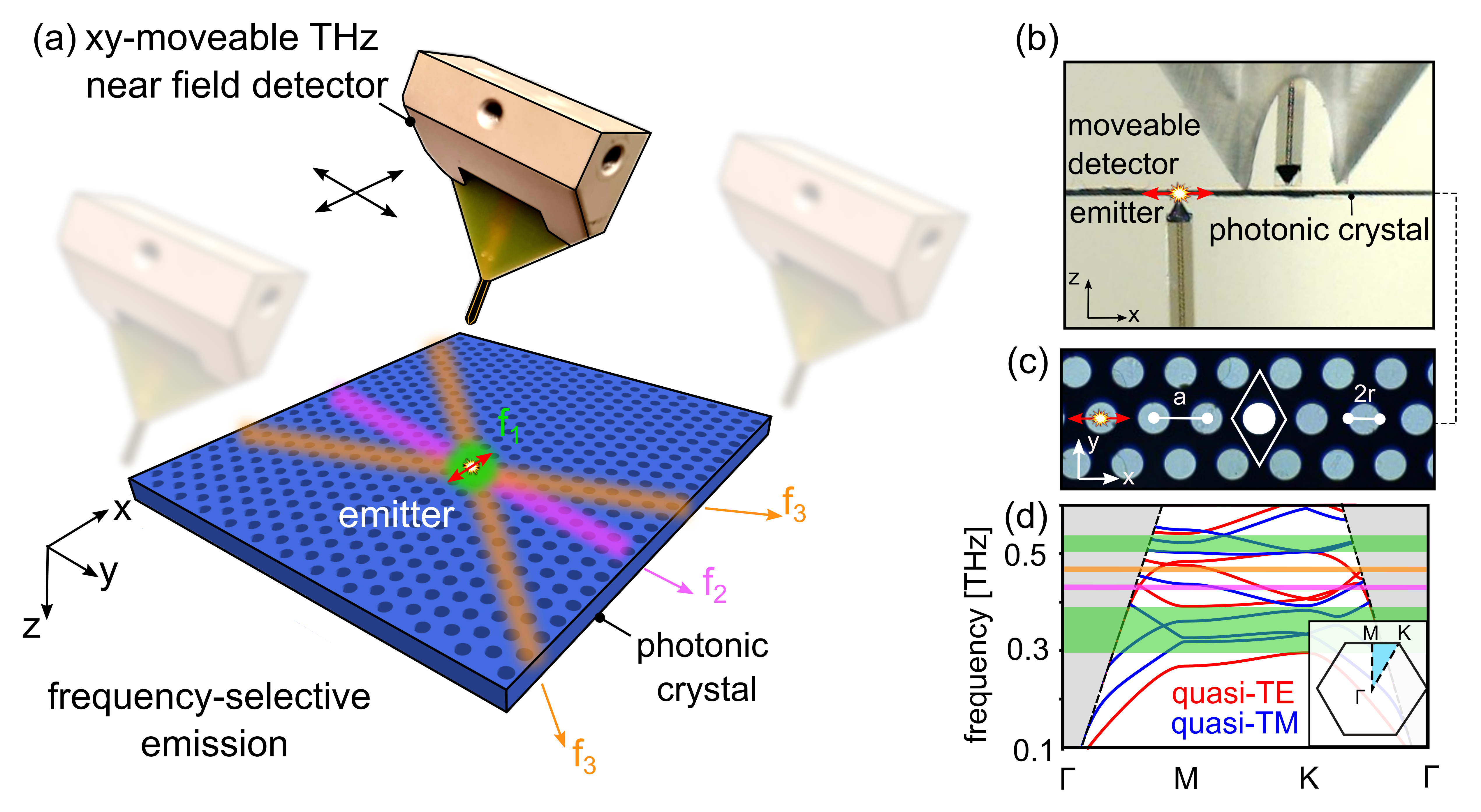
Figure 1(a) shows a schematic of our experimental configuration and approach. We consider a photonic crystal membrane composed of a silicon slab containing a hexagonal lattice of subwavelength diameter holes. A horizontally polarized broadband electric dipole (nominal emission frequency range: 0.2-2 THz) is placed near its surface. The resulting field pattern at each frequency depends on the underlying band structure, discussed below, and is measured on the surface of the photonic crystal membrane by a terahertz near-field antenna. Figure 1(b) shows a photograph of the experimental setup, which is a modified terahertz time-domain spectroscopy system 59, wherein two near-field -polarized antenna probes 60 are used as the emitter and the detector on opposite sides of the membrane, as described in the Methods section. The electric field is polarized in , using the sample orientation and reference frame shown in Fig. 1. We estimate the distance between the sample and the emitter/detector to be , which reduces the risk of sample and antenna damage during such large area scans.
Note that a similar setup was recently used to measure the terahertz Local Density of States on metal and dielectric surfaces 61, the symmetry protection properties of Bound States in the Continuum 62, and other near-field topological waveguide effects 63 – with a notable difference that here, placing the emitter and detector on opposite sides of the sample (as opposed to placing both emitter and detector on the same side 62) has two important advantages: (i) it allows us to scan the entire sample surface because we are not limited to regions that are far from the bulky emitter antenna; (ii) by detecting the evanescent field of the slab modes excited by the emitter itself, it eliminates the possibility of measuring the direct contribution of the emitted field, which is mediated by the slab modes’ surface waves. Such an approach has been reported in the microwave range, e.g., experimentally characterizing hyperbolic media 49, topological effects 64, and synthetic frequencies 65 where sources and detectors are macroscopic, but has to the best of our knowledge not been shown at THz frequencies.
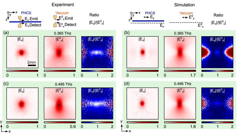
Figure 1(c) shows a micrograph of the photonic crystal, formed by hexagonally arranged air holes in float zone silicon, and fabricated using deep etching 30. The thickness of the slab is , the radius of the hole is , and the pitch from center to center is . The photonic crystal band structure, calculated using the plane-wave expansion method 66, is shown in Fig. 1(d): as expected 67, this structure has two quasi-TE band gaps at THz and THz (shaded green), which should suppress the dipole emission. Furthermore, close to the band-edge (shaded in red), we expect directed emission that subtly depends on the relative orientation of the dipole with respect to the photonic crystal lattice 42, 34. We now investigate each case in detail.
Bandgap emission suppression
We begin by considering the lowest-frequency bandgap as per Fig. 1(d). Figure 2(a) (left) shows the measured -polarized electric field amplitude detected at 0.365 THz on the sample surface, as per the top schematic. We notice a central bright region, corresponding to the location of the source on the opposite side of the sample, but no vertical diffraction on either side, suggesting that emission in the -direction has been suppressed. To confirm this, we remove the sample, leaving all other conditions unchanged, and repeat the measurements to obtain . The results are shown in the middle window of Fig. 2(a), with no emission in each -direction as expected for an -polarized dipole. To quantify the emission suppression in the bandgap, we take the ratio (right window), which clearly shows a suppression of the emission in the vertical direction. Note that, in displaying this amplitude ratio, the color scale has been chosen so that blue and red are below and above unity, respectively.
A comparison with the corresponding Finite Difference Time Domain simulation (CST Microwave Studio) is shown in Fig. 2(b). The photonic crystal was modeled as a slab with a thickness of 250 m made of dielectric with a refractive index 29 between 0.3 – 0.50 THz, containing hexagonally arranged holes with diameter and pitch as in our sample specifications, using a slab area of 1 cm 1 cm and open boundary conditions in the - and - directions. The -polarized dipole source and the electric field detector are located at a distance of 200 µm, on opposite sides of the photonic crystal surface, for fair comparison with experiments. The corresponding is obtained by considering the same simulation space without the photonic crystal. We find excellent agreement between the experiment and simulation, confirming the dipole emission suppression in due to the TE-band gap.
The large bandwidth of our terahertz probe also allows us to probe the emission suppression at the second quasi-TE bandgap at 0.495 THz (see Fig. 2(c)), half an octave higher in frequency. Figure 2(c) and (d) show the corresponding experiment and simulations at that frequency, both showing emission suppression, in excellent agreement with each other. These experiments reveal the possibility of achieving a comparable and tailored (here: suppressed) emission profile over distinct and widely separated frequency bands, all using the same sample.
Band-edge directed emission and field concentration
As a next step, we consider the emission profile of two frequencies close to the lower edge of the second quasi-TE bandgap (0.45 THz). It is well known that in these regions self-guiding 43 or directed emission 42, 34 are supported, depending on whether the source is a collimated beam or a point dipole. Such behavior is a notoriously narrow band 43, and therefore highly sensitive to any fabrication-induced deviations from the numerical design, thus requiring accurate experimental measurements after fabrication to complement the design phase. Here the large bandwidth of the THz source allows us to scan all frequencies in this region to identify at which frequencies directed emission occurs.
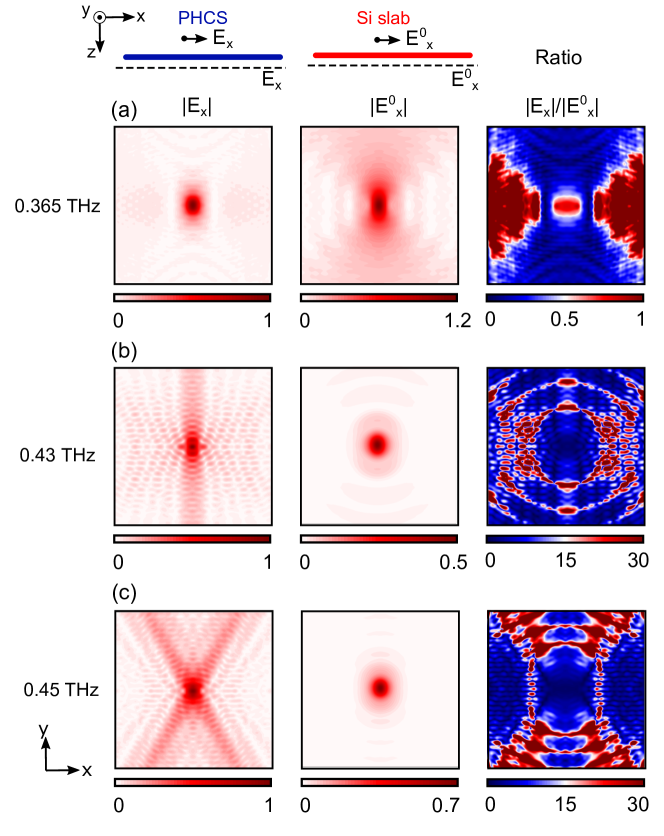
Figure 3 shows the results of the same experiments and simulations shown in Fig. 2 but in a different spectral region. Figure 3(a) (left) shows the measured -polarized electric field amplitude detected at 0.445 THz on the sample surface, for a PC unit cell oriented as shown on the left-most column, here showing strong vertical directed emission and weak emission in two diagonal regions. Taking the ratio with respect to the dipole intensity pattern with the sample removed (Fig. 3(b), middle) clearly shows a field concentration along the vertical and diagonal regions (Fig. 3(b), middle). Note in particular that the field is concentrated by a factor of two along the vertical region (i.e., ), as opposed to mere spatial filtering. This corresponds to an increase of 6 dB in field intensity, despite the presence of the silicon. Simulations indicate that, compared to a bare silicon slab, the relative field concentration in the photonic crystal slab is even greater – of order 10-30 times – as illustrated in Figure S1 of the Supporting Information.
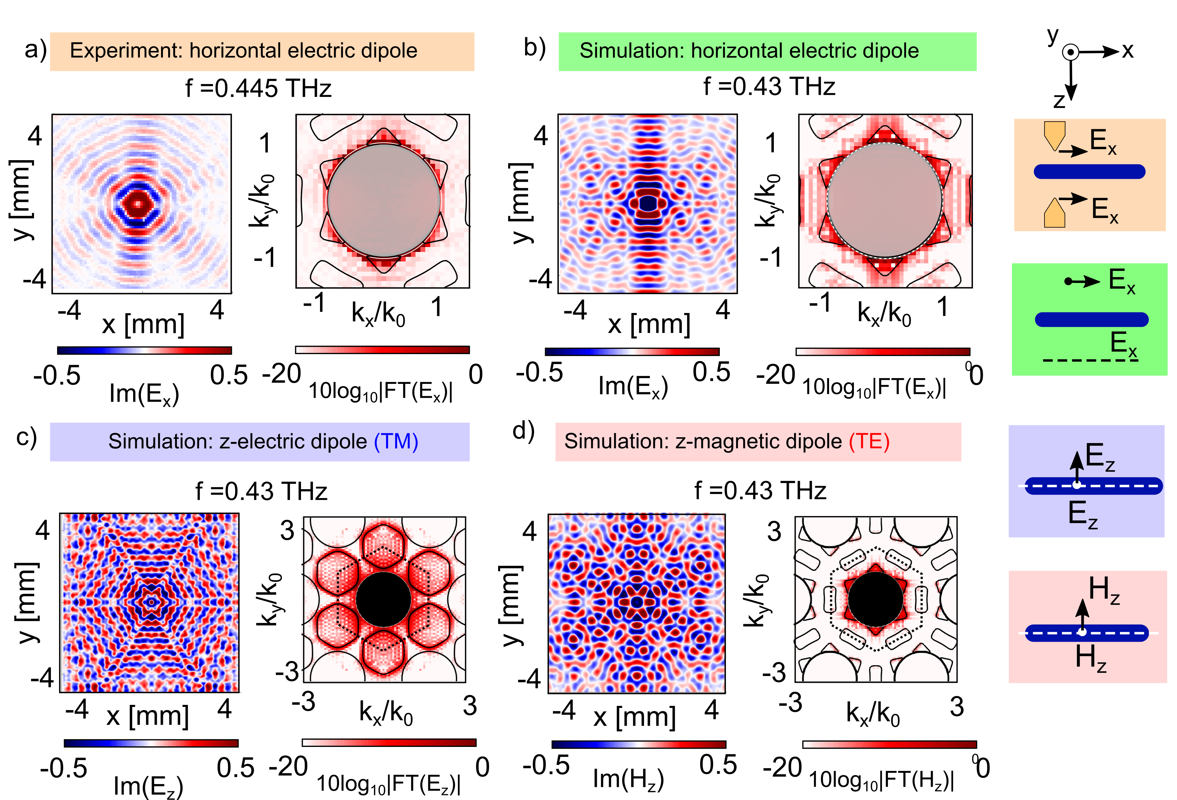
These measurements are in good agreement with simulations at 0.43 THz, which is 0.015 THz from the measured frequency, most likely due to the extreme sensitivity of these effects to any small deviations in the sample from the ideal design (e.g., imperfections in the fabrication process, difference in hole size, pitch, slab thickness, and refractive index). The associated frequency contours for the quasi-TE modes (red) and quasi-TM modes (blue), shown in Fig. 3(c), allow us to interpret the observed behavior: a horizontally polarized dipole (black arrow) excites quasi-TE Bloch modes with a nearly flat contour close to the light line at , corresponding to vertical emission. Note, the diagonal quasi-TE modes near the light line (black dashed line) at are also excited, albeit more weakly, due to a smaller overlap between the point dipole field pattern and the diagonally-directed Bloch modes. Our analysis is consistent with simulations that consider the 2D Fourier transforms of the measured complex fields, which overlap well with the simulated isofrequency contours, as shown Figure S2 of the Supporting Information.
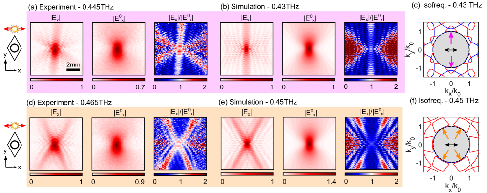
Finally, we consider field amplitude measurements at a slightly higher frequency (0.465 THz), shown in Fig. 3(d). In this case, we observe emission along two diagonal axes, now forming an “X”-shaped pattern (left), i.e., the emission direction is rotated by with respect to the case in Fig. 3(a). After considering the bare dipole (middle), the associated ratio (right) reveals directed emission and field concentration (as opposed to mere filtering) along the diagonal direction (red regions), in good agreement with the corresponding simulations at 0.45 THz shown in Fig. 3(e). The associated calculated isofrequency contour, shown in Fig. 3(f) now reveals that there are only quasi-TE Bloch modes (red line) that are close to the light line, and which are rotated by with respect to those shown in Fig. 3(c) and highlighted by the orange arrows pointing to . Note that in this case, the overlap integral between the -polarized dipole and the quasi-TE Bloch modes at is zero so that no field is emitted along .
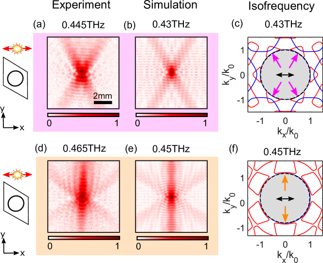
The above experiments and analysis immediately suggest a pathway for redirecting the field emitted by the point dipole, simply by rotating the photonic crystal 34. Figure 4(a) (left) shows the measured -polarized electric field amplitude, , detected at a 0.445 THz on the sample surface, when the photonic crystal unit cell is rotated by with respect to Fig. 3, as shown by the left-most schematics of Fig. 4. In this configuration, and in contrast to the results shown in Fig. 3, we observe an “X” shaped emission pattern at this frequency, in agreement with the simulations at 0.43 THz shown in Fig. 4(b). This result is an immediate consequence of the associated rotation of the isofrequency contours, as shown in Fig. 4(c). As a result, the slightly higher frequency of 0.465 THz shows a predominantly -directed emission (Fig. 4(d)), in agreement with simulations (Fig. 4(e)), because of the associated rotated isofrequency contour (Fig. 4(f)). This clearly indicates that we can control the emission direction not only by changing the excitation frequency but also by altering the polarization of the source dipole with respect to the photonic crystal orientation, providing potential additional avenues for both space- and frequency-division multiplexing on a single chip-based platform.
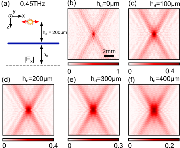
Note that in our experimental configuration, the emitter and detector antenna are placed at a distance from the edge of the photonic crystal such that it lies in the radiating near-field (i.e., such that 68). At this position, the higher- Bloch modes cannot be accessed, as shown by additional simulations in Fig. S2 of the Supporting Information, which also considers the 2D Fourier transforms of the measured complex fields. The higher- Bloch modes can be accessed by placing appropriately polarized dipoles inside the photonic crystal, as shown in Fig. S2 of the Supporting Information, but are inaccessible under the current experimental configurations, and which would, in any case, excite unwanted high- modes and thus be detrimental to directional emission in the present context. Finally, our simulations suggest that the salient features of the measured images are only weakly dependent on the detector distance, provided that it is within approximately one wavelength of the sample surface. The dependence of the field pattern with respect to the detector’s -position is shown in Fig. S3 in the Supporting Information.
3 Conclusion
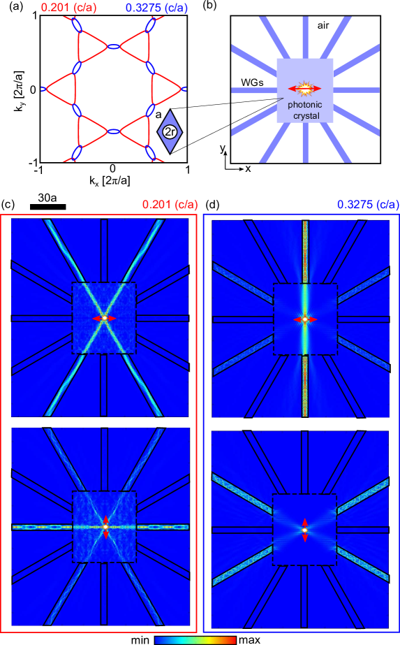
Photonic crystal membranes are a powerful tool to suppress, concentrate, and redirect the field emitted by terahertz antennas when they are placed close to their surface. To demonstrate this, we developed a novel terahertz near-field emission/detection setup that relies on placing each antenna on opposite sides of the sample. Our approach is generally suited to characterize the subtle and sensitive directional emission properties of any planar geometry. In this particular case, our near-field measurements revealed a reduction in the emitted field inside two bandgaps at 0.35 THz and 0.5 THz. Additionally, we observed and explained a previously unreported phenomenon of directional emission and field concentration along either vertical- and diagonal- directions for two frequency channels near 0.455 THz, spaced only 20 GHz apart. The signals were then re-oriented simply by rotating the relative axis of the dipole orientation and underlying photonic crystal. Our results show that bulk photonic crystals provide a potential pathway for simple short-haul 6G circuit elements without needing any additional defects or materials, and which could, for example, be directly connectorized to suspended silicon waveguides. Future designs might consider integrating several terahertz dipole antennas on photonic crystal surfaces to direct distinct polarizations along separate spatial channels at different frequencies. Connecting these channels to waveguides at the edge of the chip would then form a monolithic frequency-dependent power splitter – Fig. S4 in the Supporting Information shows a numerical example illustrating its operation using an analogous two-dimensional photonic crystal connected to surrounding step index waveguides. Our approach uses the frequency-dependent photonic crystal band structure, which provides a much richer parameter space than simple waveguides, whose geometry dictates the direction of light propagation at all frequencies. Changing the hole size and spacing throughout the chip could provide additional flexibility with regards to the accessible frequencies for directed emission, within the symmetry constraints of the photonic crystal. Related application examples that warrant revisiting and detailed near field experimental characterization at terahertz frequencies include wavelength-dependent self-guidance 69, polarization dependent splitting 70 and multiplexing 71.
Our experiments suggest that wider classes of photonic structures, for example, square photonic crystals 42, topologically protected edge states 21, Dirac points 72, or hyperbolic media 73, likely provide many opportunities for controlling the emission of terahertz antennas in unexpected ways. Due to the extreme sensitivity of photonic crystal band structures to specific designs, our experimental technique will provide a valuable tool for refining device development due to practical limits during fabrication. In the field of quantum optics, strongly modified emission properties induced by the photonic crystal might also be used to mediate the strong anisotropic dipole–dipole coupling of individual quantum emitters 34, the development of which at terahertz frequencies is in a nascent stage 74, 75. More broadly, this terahertz near-field excitation and detection scheme – which uniquely measures evanescent fields mediated by slab modes over the entire sample surface – may provide a useful and versatile tool for better understanding or revealing new physics over broad bandwidths, particularly in situations where large-scale numerical simulations become prohibitively slow and computationally demanding.
4 Methods
4.1 Terahertz near field emission and detection
We use a commercially available THz Time Domain Spectroscopy (THz-TDS) System (Menlo TERAK15), which relies on THz emission from biased photoconductive antennas (Protemics) that are pumped by fiber-coupled near-infrared pulses (pulse width: 90 fs; wavelength: 1560 nm) in combination with a second harmonic generaion (SHG) module (Protemics) which converts the laser to 780 nm to excite the low temperature GaAs photocurrent needed for terahertz generation. The field emitted by the terahertz antenna couples to the Bloch modes of the photonic crystal. On the other side of the sample, the resulting field is sampled as a function of the time delay via an infrared probe pulse on another identical near-field photoconductive antenna module, placed on a movable stage, which forms the THz detector. The near-field is thus spatio-temporally resolved at every point via a raster scan (step size: ; window size: ) with sub-THz cycle temporal resolution, so that Fast Fourier transforms of the temporal response at each pixel position provide the spectral information, including amplitude and phase.
Acknowledgments
This work is funded in part by the Australian Research Council Discovery Early Career Researcher Award (DE200101041) and Future Fellowship (FT200100844). This work was performed in part at the NSW node of the Australian Nanofabrication Facility. This research was conducted within the context of the International Associated Laboratory “ALPhFA: Associated Laboratory for Photonics between France and Australia”. We gratefully acknowledge Gloria Qiu and Jackie He from the University of Sydney Research and Prototype Foundry for assistance with sample fabrication, and Alex Y. Song for fruitful discussions.
References
- Jepsen et al. 2011 Jepsen, P. U.; Cooke, D. G.; Koch, M. Terahertz spectroscopy and imaging–Modern techniques and applications. Laser & Photonics Reviews 2011, 5, 124–166
- Markelz and Mittleman 2022 Markelz, A. G.; Mittleman, D. M. Perspective on terahertz applications in bioscience and biotechnology. ACS Photonics 2022, 9, 1117–1126
- Smolyanskaya et al. 2018 Smolyanskaya, O. et al. Terahertz biophotonics as a tool for studies of dielectric and spectral properties of biological tissues and liquids. Progress in Quantum Electronics 2018, 62, 1–77
- Lee et al. 2022 Lee, G.; Lee, J.; Park, Q.-H.; Seo, M. Frontiers in Terahertz Imaging Applications beyond Absorption Cross-Section and Diffraction Limits. ACS Photonics 2022, 9, 1500–1512
- Seo and Kim 2022 Seo, C.; Kim, T.-T. Terahertz near-field spectroscopy for various applications. Journal of the Korean Physical Society 2022, 81, 549–561
- Siegel 2007 Siegel, P. H. THz instruments for space. IEEE Transactions on Antennas and Propagation 2007, 55, 2957–2965
- Kleine-Ostmann and Nagatsuma 2011 Kleine-Ostmann, T.; Nagatsuma, T. A review on terahertz communications research. Journal of Infrared, Millimeter, and Terahertz Waves 2011, 32, 143–171
- Yang and Jarrahi 2020 Yang, S.-H.; Jarrahi, M. Navigating terahertz spectrum via photomixing. Optics and Photonics News 2020, 31, 36–43
- Mamaghani and Hong 2022 Mamaghani, M. T.; Hong, Y. Aerial intelligent reflecting surface-enabled terahertz covert communications in beyond-5G Internet of Things. IEEE Internet of Things Journal 2022, 9, 19012–19033
- Headland et al. 2021 Headland, D.; Withayachumnankul, W.; Fujita, M.; Nagatsuma, T. Gratingless integrated tunneling multiplexer for terahertz waves. Optica 2021, 8, 621
- Tan et al. 2023 Tan, Z.; Zhang, Q.; Lei, Y.; Zhao, Y.; Ding, J. Terahertz waveguide multiplexers: A review. Microwave and Optical Technology Letters 2023, 65, 1925–1935
- Pang et al. 2022 Pang, X.; Ozolins, O.; Jia, S.; Zhang, L.; Schatz, R.; Udalcovs, A.; Bobrovs, V.; Hu, H.; Morioka, T.; Sun, Y.-T.; others Bridging the terahertz gap: Photonics-assisted free-space communications from the submillimeter-wave to the mid-infrared. Journal of Lightwave Technology 2022, 40, 3149–3162
- Ma et al. 2018 Ma, J.; Shrestha, R.; Moeller, L.; Mittleman, D. M. Invited article: Channel performance for indoor and outdoor terahertz wireless links. APL Photonics 2018, 3, 051601
- Federici et al. 2016 Federici, J. F.; Ma, J.; Moeller, L. Review of weather impact on outdoor terahertz wireless communication links. Nano Communication Networks 2016, 10, 13–26
- Shrestha et al. 2022 Shrestha, R.; Guerboukha, H.; Fang, Z.; Knightly, E.; Mittleman, D. M. Jamming a terahertz wireless link. Nature Communications 2022, 13, 3045
- Shams and Seeds 2017 Shams, H.; Seeds, A. Photonics, fiber and THz wireless communication. Optics and Photonics News 2017, 28, 24–31
- Piesiewicz et al. 2008 Piesiewicz, R.; Jacob, M.; Koch, M.; Schoebel, J.; Kurner, T. Performance analysis of future multigigabit wireless communication systems at THz frequencies with highly directive antennas in realistic indoor environments. IEEE Journal of selected topics in quantum electronics 2008, 14, 421–430
- Xu and Skorobogatiy 2022 Xu, G.; Skorobogatiy, M. Wired THz Communications. Journal of Infrared, Millimeter, and Terahertz Waves 2022, 43, 728–778
- Koala et al. 2022 Koala, R. A. S. D.; Fujita, M.; Nagatsuma, T. Nanophotonics-inspired all-silicon waveguide platforms for terahertz integrated systems. Nanophotonics 2022, 11, 1741–1759
- Tsuruda et al. 2015 Tsuruda, K.; Fujita, M.; Nagatsuma, T. Extremely low-loss terahertz waveguide based on silicon photonic-crystal slab. Optics Express 2015, 23, 31977–31990
- Yang et al. 2020 Yang, Y.; Yamagami, Y.; Yu, X.; Pitchappa, P.; Webber, J.; Zhang, B.; Fujita, M.; Nagatsuma, T.; Singh, R. Terahertz topological photonics for on-chip communication. Nature Photonics 2020, 14, 446–451
- Headland et al. 2020 Headland, D.; Withayachumnankul, W.; Yu, X.; Fujita, M.; Nagatsuma, T. Unclad microphotonics for terahertz waveguides and systems. Journal of Lightwave Technology 2020, 38, 6853–6862
- Islam et al. 2020 Islam, M. S.; Cordeiro, C. M.; Franco, M. A.; Sultana, J.; Cruz, A. L.; Abbott, D. Terahertz optical fibers. Optics Express 2020, 28, 16089–16117
- Nielsen et al. 2009 Nielsen, K.; Rasmussen, H. K.; Adam, A. J.; Planken, P. C.; Bang, O.; Jepsen, P. U. Bendable, low-loss Topas fibers for the terahertz frequency range. Optics Express 2009, 17, 8592–8601
- Stefani et al. 2021 Stefani, A.; Skelton, J. H.; Tuniz, A. Bend losses in flexible polyurethane antiresonant terahertz waveguides. Optics Express 2021, 29, 28692–28703
- Weidenbach et al. 2016 Weidenbach, M.; Jahn, D.; Rehn, A.; Busch, S.; Beltrán-Mejía, F.; Balzer, J.; Koch, M. 3D printed dielectric rectangular waveguides, splitters and couplers for 120 GHz. Optics Express 2016, 24, 28968–28976
- Yata et al. 2016 Yata, M.; Fujita, M.; Nagatsuma, T. Photonic-crystal diplexers for terahertz-wave applications. Optics Express 2016, 24, 7835–7849
- Cao et al. 2022 Cao, Y.; Nallappan, K.; Xu, G.; Skorobogatiy, M. Add drop multiplexers for terahertz communications using two-wire waveguide-based plasmonic circuits. Nature Communications 2022, 13, 4090
- Dai et al. 2004 Dai, J.; Zhang, J.; Zhang, W.; Grischkowsky, D. Terahertz time-domain spectroscopy characterization of the far-infrared absorption and index of refraction of high-resistivity, float-zone silicon. Journal of the Optical Society of America B 2004, 21, 1379–1386
- Brückner et al. 2009 Brückner, C.; Käsebier, T.; Pradarutti, B.; Riehemann, S.; Notni, G.; Kley, E.-B.; Tünnermann, A. Broadband antireflective structures applied to high resistive float zone silicon in the THz spectral range. Optics Express 2009, 17, 3063–3077
- Headland et al. 2021 Headland, D.; Withayachumnankul, W.; Fujita, M.; Nagatsuma, T. Gratingless integrated tunneling multiplexer for terahertz waves. Optica 2021, 8, 621–629
- Cong et al. 2018 Cong, L.; Srivastava, Y. K.; Zhang, H.; Zhang, X.; Han, J.; Singh, R. All-optical active THz metasurfaces for ultrafast polarization switching and dynamic beam splitting. Light: Science & Applications 2018, 7, 28
- Liu et al. 2021 Liu, W.; Yang, Q.; Xu, Q.; Jiang, X.; Wu, T.; Wang, K.; Gu, J.; Han, J.; Zhang, W. Multifunctional All-Dielectric Metasurfaces for Terahertz Multiplexing. Advanced Optical Materials 2021, 9, 2100506
- Yu et al. 2019 Yu, S.-P.; Muniz, J. A.; Hung, C.-L.; Kimble, H. Two-dimensional photonic crystals for engineering atom–light interactions. Proceedings of the National Academy of Sciences 2019, 116, 12743–12751
- Yermakov et al. 2018 Yermakov, Y.; Hurshkainen, A. A.; Dobrykh, D. A.; Kapitanova, P. V.; Iorsh, I. V.; Glybovski, S. B.; Bogdanov, A. A. Experimental observation of hybrid TE-TM polarized surface waves supported by a hyperbolic metasurface. Physical Review B 2018, 98, 195404
- Noda et al. 2007 Noda, S.; Fujita, M.; Asano, T. Spontaneous-emission control by photonic crystals and nanocavities. Nature Photonics 2007, 1, 449–458
- Hoeppe et al. 2012 Hoeppe, U.; Wolff, C.; Küchenmeister, J.; Niegemann, J.; Drescher, M.; Benner, H.; Busch, K. Direct observation of non-Markovian radiation dynamics in 3D bulk photonic crystals. Physical Review Letters 2012, 108, 043603
- Kounoike et al. 2005 Kounoike, K.; Yamaguchi, M.; Fujita, M.; Asano, T.; Nakanishi, J.; Noda, S. Investigation of spontaneous emission from quantum dots embedded in two-dimensional photonic-crystal slab. Electronics Letters 2005, 41, 1402–1403
- Iliew et al. 2004 Iliew, R.; Etrich, C.; Peschel, U.; Lederer, F.; Augustin, M.; Fuchs, H.-J.; Schelle, D.; Kley, E.-B.; Nolte, S.; Tünnermann, A. Diffractionless propagation of light in a low-index photonic-crystal film. Applied Physics Letters 2004, 85, 5854–5856
- Kosaka et al. 1999 Kosaka, H.; Kawashima, T.; Tomita, A.; Notomi, M.; Tamamura, T.; Sato, T.; Kawakami, S. Self-collimating phenomena in photonic crystals. Applied Physics Letters 1999, 74, 1212–1214
- Rakich et al. 2006 Rakich, P. T.; Dahlem, M. S.; Tandon, S.; Ibanescu, M.; Soljačić, M.; Petrich, G. S.; Joannopoulos, J. D.; Kolodziejski, L. A.; Ippen, E. P. Achieving centimetre-scale supercollimation in a large-area two-dimensional photonic crystal. Nature Materials 2006, 5, 93–96
- Chigrin et al. 2003 Chigrin, D. N.; Enoch, S.; Torres, C. M. S.; Tayeb, G. Self-guiding in two-dimensional photonic crystals. Optics Express 2003, 11, 1203–1211
- Yu and Fan 2003 Yu, X.; Fan, S. Bends and splitters for self-collimated beams in photonic crystals. Applied Physics Letters 2003, 83, 3251–3253
- Gralak et al. 2000 Gralak, B.; Enoch, S.; Tayeb, G. Anomalous refractive properties of photonic crystals. Journal of the Optical Society of America A 2000, 17, 1012–1020
- Matthews et al. 2007 Matthews, A. F.; Morrison, S. K.; Kivshar, Y. S. Self-collimation and beam splitting in low-index photonic crystals. Optics Communications 2007, 279, 313–319
- Zhaolin Lu et al. 2005 Zhaolin Lu; Schuetz, C.; Shouyuan Shi; Caihua Chen; Behrmann, G.; Prather, D. Experimental demonstration of self-collimation in low-index-contrast photonic crystals in the millimeter-wave regime. IEEE Transactions on Microwave Theory and Techniques 2005, 53, 1362–1368
- Lu et al. 2006 Lu, Z.; Shi, S.; Murakowski, J. A.; Schneider, G. J.; Schuetz, C. A.; Prather, D. W. Experimental Demonstration of Self-Collimation inside a Three-Dimensional Photonic Crystal. Physical Review Letters 2006, 96, 173902
- Combrié et al. 2009 Combrié, S.; De Rossi, A.; others Directive emission from high-Q photonic crystal cavities through band folding. Physical Review B 2009, 79, 041101
- Yermakov et al. 2018 Yermakov, O. Y.; Hurshkainen, A. A.; Dobrykh, D. A.; Kapitanova, P. V.; Iorsh, I. V.; Glybovski, S. B.; Bogdanov, A. A. Experimental observation of hybrid TE-TM polarized surface waves supported by a hyperbolic metasurface. Physical Review B 2018, 98, 195404
- Martínez et al. 2006 Martínez, A.; Piqueras, M. A.; Martí, J. Generation of highly directional beam by k-space filtering using a metamaterial flat slab with a small negative index of refraction. Applied Physics Letters 2006, 89
- Le Feber et al. 2014 Le Feber, B.; Rotenberg, N.; Beggs, D. M.; Kuipers, L. Simultaneous measurement of nanoscale electric and magnetic optical fields. Nature Photonics 2014, 8, 43–46
- Rotenberg and Kuipers 2014 Rotenberg, N.; Kuipers, L. Mapping nanoscale light fields. Nature Photonics 2014, 8, 919–926
- Matthews 2009 Matthews, A. F. Experimental demonstration of self-collimation beaming and splitting in photonic crystals at microwave frequencies. Optics Communications 2009, 282, 1789–1792
- Trull et al. 2011 Trull, J.; Maigyte, L.; Mizeikis, V.; Malinauskas, M.; Juodkazis, S.; Cojocaru, C.; Rutkauskas, M.; Peckus, M.; Sirutkaitis, V.; Staliunas, K. Formation of collimated beams behind the woodpile photonic crystal. Physical Review A 2011, 84, 033812
- Bulu et al. 2003 Bulu, I.; Caglayan, H.; Ozbay, E. Highly directive radiation from sources embedded inside photonic crystals. Applied Physics Letters 2003, 83, 3263–3265
- Yarga et al. 2008 Yarga, S.; Sertel, K.; Volakis, J. L. Degenerate band edge crystals for directive antennas. IEEE transactions on antennas and propagation 2008, 56, 119–126
- Bulu et al. 2005 Bulu, I.; Caglayan, H.; Aydin, K.; Ozbay, E. Compact size highly directive antennas based on the SRR metamaterial medium. New Journal of Physics 2005, 7, 223
- Kosaka et al. 1998 Kosaka, H.; Kawashima, T.; Tomita, A.; Notomi, M.; Tamamura, T.; Sato, T.; Kawakami, S. Superprism phenomena in photonic crystals. Physical review B 1998, 58, R10096
- Stefani et al. 2022 Stefani, A.; Kuhlmey, B. T.; Digweed, J.; Davies, B.; Ding, Z.; Zreiqat, H.; Mirkhalaf, M.; Tuniz, A. Flexible Terahertz Photonic Light-Cage Modules for In-Core Sensing and High Temperature Applications. ACS Photonics 2022, 9, 2128–2141
- 60 Protemics website. https://www.protemics.com/, [Accessed: 27-October-2022]
- ter Huurne et al. 2023 ter Huurne, S. E.; Peeters, D. B.; Sánchez-Gil, J. A.; Rivas, J. G. Direct Measurement of the Local Density of Optical States in the Time Domain. ACS Photonics 2023, 10, 2980–2986
- van Hoof et al. 2021 van Hoof, N. J.; Abujetas, D. R.; Ter Huurne, S. E.; Verdelli, F.; Timmermans, G. C.; Sánchez-Gil, J. A.; Rivas, J. G. Unveiling the Symmetry Protection of Bound States in the Continuum with Terahertz Near-Field Imaging. ACS Photonics 2021, 8, 3010–3016
- Yang et al. 2022 Yang, Q.; Wang, D.; Kruk, S.; Liu, M.; Kravchenko, I.; Han, J.; Kivshar, Y.; Shadrivov, I. Topology-empowered membrane devices for terahertz photonics. Advanced Photonics 2022, 4, 046002
- Yang et al. 2018 Yang, B.; Guo, Q.; Tremain, B.; Liu, R.; Barr, L. E.; Yan, Q.; Gao, W.; Liu, H.; Xiang, Y.; Chen, J.; others Ideal Weyl points and helicoid surface states in artificial photonic crystal structures. Science 2018, 359, 1013–1016
- Guan et al. 2023 Guan, F.; Guo, X.; Zeng, K.; Zhang, S.; Nie, Z.; Ma, S.; Dai, Q.; Pendry, J.; Zhang, X.; Zhang, S. Overcoming losses in superlenses with synthetic waves of complex frequency. Science 2023, 381, 766–771
- Minkov et al. 2020 Minkov, M.; Williamson, I. A.; Andreani, L. C.; Gerace, D.; Lou, B.; Song, A. Y.; Hughes, T. W.; Fan, S. Inverse design of photonic crystals through automatic differentiation. ACS Photonics 2020, 7, 1729–1741
- Joannopoulos et al. 2008 Joannopoulos, J. D.; Johnson, S. G.; Winn, J. N.; Meade, R. D. Photonic Crystals: Molding the Flow of Light (Second Edition); Princeton University Press, 2008; Chapter 8
- Yaghjian 1986 Yaghjian, A. An overview of near-field antenna measurements. IEEE Transactions on antennas and propagation 1986, 34, 30–45
- Turduev et al. 2013 Turduev, M.; Giden, I. H.; Kurt, H. Extraordinary wavelength dependence of self-collimation effect in photonic crystal with low structural symmetry. Photonics and Nanostructures-Fundamentals and Applications 2013, 11, 241–252
- Yasa et al. 2017 Yasa, U. G.; Giden, I.; Turduev, M.; Kurt, H. Polarization splitting phenomenon of photonic crystals constructed by two-fold rotationally symmetric unit-cells. Journal of Optics 2017, 19, 095005
- Ito et al. 2018 Ito, H.; Tatebe, T.; Abe, H.; Baba, T. Wavelength-division multiplexing Si photonic crystal beam steering device for high-throughput parallel sensing. Optics Express 2018, 26, 26145–26155
- Bittner et al. 2010 Bittner, S.; Dietz, B.; Miski-Oglu, M.; Iriarte, P. O.; Richter, A.; Schäfer, F. Observation of a Dirac point in microwave experiments with a photonic crystal modeling graphene. Physical Review B 2010, 82, 014301
- Tuniz et al. 2013 Tuniz, A.; Kaltenecker, K. J.; Fischer, B. M.; Walther, M.; Fleming, S. C.; Argyros, A.; Kuhlmey, B. T. Metamaterial fibres for subdiffraction imaging and focusing at terahertz frequencies over optically long distances. Nature Communications 2013, 4, 2706
- Kibis et al. 2009 Kibis, O.; Slepyan, G. Y.; Maksimenko, S.; Hoffmann, A. Matter coupling to strong electromagnetic fields in two-level quantum systems with broken inversion symmetry. Physical Review Letters 2009, 102, 023601
- 75 Groiseau, C.; Domínguez, A. I. F.; Cano, D. M.; Muñoz, C. S. Single-photon source over the terahertz regime. 19 May 2023. arXiv:2305.11754, (Accessed: 2023-09-01)
Supporting Information