The Superconducting Quasiparticle-Amplifying Transmon: A Qubit-Based Sensor for meV Scale Phonons and Single THz Photons
Abstract
With great interest from the quantum computing community, an immense amount of R&D effort has been invested into improving superconducting qubits. The technologies developed for the design and fabrication of these qubits can be directly applied to applications for ultra-low threshold particle detectors, e.g. low-mass dark matter and far-IR photon sensing. We propose a novel energy resolving sensor based on the transmon qubit architecture combined with a signal-enhancing superconducting quasiparticle amplification stage. We refer to these sensors as SQUATs: Superconducting Quasiparticle-Amplifying Transmons. We detail the operating principle and design of this new sensor and predict that with minimal R&D effort, solid-state based detectors patterned with these sensors can achieve sensitivity to single THz photons, and sensitivity to phonons in the detector absorber substrate on the timescale.
Introduction—The increasing maturity of superconducting qubits over the past few decades has allowed the field of superconducting quantum computing to flourish, producing a massive industry centered on the goal of improving quantum coherence. Breakthrough studies in the last few years have shown that environmental radioactivity can induce correlated errors in qubit arrays [1, 2, 3], and subsequent work has demonstrated that charge noise and phonon-induced drops in coherence time can be mitigated by designing phonon sinks and reducing photon coupling to films nearest to the qubits [4, 5].
In parallel, advances in detector technology that have built on this wave of qubit fabrication expertise have shown that this same technology can be applied to energy sensing at the THz (meV) scale. The first demonstration of the Quantum Capacitance Detector (QCD) [6, 7] showed that single THz photon detection can be achieved by utilizing a Cooper pair box coupled to a resonator – a structure analogous to many early charge-sensitive qubits. This demonstration and work to understand the radiation sensitivity of qubits have opened up a new regime of sensing leveraging the single quasiparticle (QP) sensitivity of qubit-derived structures. The main sensing mechanism comes from the quantized nature of the qubit and the charge sensitivity of the transition, such that a single quasiparticle tunneling across the junction is easily measurable in real time [8, 9, 10, 11]. If energy can be focused into breaking Cooper pairs near the junction, as is done in Ref [7], then very low thresholds are achievable.
In this letter we propose a novel sensing technology based on weakly charge-coupled transmon qubits. The scheme described in this paper differs from the QCD design [6, 7] and that of conventional superconducting qubits [12, 13, 14, 15, 16, 2] by removing the readout resonator entirely from the architecture and relying on direct readout of the qubit transition frequency to detect tunneling events. By removing the readout resonator, we are no longer sensitive to the quantum capacitance as in the QCD, but rather we are sensitive to the quantum inductance in the non-linear LC resonator that makes up the qubit. This architecture change allows for significant reduction in the overall size of the unit cell, increases in pixel density, reduction of two-level system noise, and increase in detection efficiency for uniformly distributed radiation signals. We will show that these devices should outperform the energy sensitivity of competing technologies, while the RF based readout scheme allows them to be naturally multiplexed, thus allowing for highly pixalizable, ultra-low threshold single THz photon and single-phonon detection.
Operating Principle—Transmon qubits [12] are anharmonic LC oscillators where the capacitance comes from the proximity of metal islands that are connected by a Josephson junction (JJ), which provides a nonlinear inductance. The nonlinearity of the inductance creates unequally spaced energy levels; typical qubit operation uses only the first two levels, the ground, , and first excited, , states.
The energy difference between these states, , also called the splitting energy, is dependent on the qubit’s design, parametrized by the qubit’s charging energy, , the energy to increment the qubit’s charge by one electron, and the Josephson energy, , the tunneling energy of a Cooper pair. In the transmon limit, which corresponds to , we can model the energy spectrum of the qubit accurately as [12]
| (1) |
where is the island charge,
| (2) |
and
| (3) | ||||
| (4) | ||||
| (5) |
controls the magnitude of the charge dependence of the splitting. We can thus tune the qubit to a given frequency by careful design of the junction area and critical current density, as well as the total capacitance within the qubit geometry. One feature of the nonlinearity of the relationship between and and is that the qubit energy has a periodic dependence on the number of charges on the island, . Incrementing this charge by one electron switches the state parity as the cosine in Eq. 1 changes phase by .
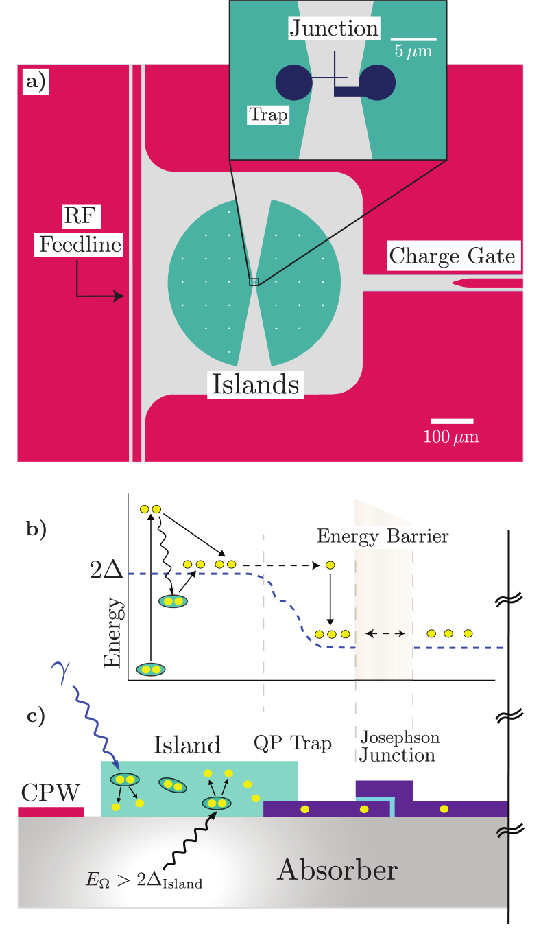
There are two ways to create non-equilibrium quasiparticles in the qubit islands, as shown in Fig. 1. First, direct energy deposition in the island produces a hot pair of quasiparticles, which quickly generate a larger quasiparticle population as they settle to the superconducting energy gap. This is the case for photon absorption or direct collision of particles with the qubit island. Alternatively, athermal substrate phonons with energies large compared to the superconducting gap of the islands will similarly excite non-equilibrium QPs in the islands. Both processes lead to the same optimization for collecting the resulting quasiparticles, but the two energy absorption methods require different considerations for external quantum efficiency, as described in the following sections.
Phonon coupling—Energetic electrons/holes or optical phonons created from an inital particle interaction in the substrate will rapidly downconvert to high energy acoustic athermal phonons. These phonons then undergo anharmonic decay until their mean free path is on the order of the characteristic size of the substrate [17]. The phonons will travel ballistically in the substrate until being absorbed by the active (sensor) and passive (e.g. RF feedline, ground plane) metal films on the surface of the substrate. From [18], the characteristic time scale for these phonon event signals can be approximated by
| (6) |
where is the volume of the substrate, is the average sound speed in the substrate, is the area of the absorbing material on the detector surface, and is the phonon transmission probability between the substrate and the absorbing material, modeled simply as
| (7) |
where is the absorber film thickness, is the sound speed in the film, and is the quasiparticle pair breaking rate, which can be found in [19] for Al and Nb.
There are two signal efficiency penalties that must be accounted for in this step. The first is the percentage of ballistic phonons with energy greater than twice the superconducting bandgap () of the sensor material, which is typically for common materials [20]. Secondly, we must account for the percentage of phonons that are absorbed by the non-instrumented areas of the detector surface. This efficiency factor can be calculated using :
| (8) |
With our initial design we expect to achieve a fill factor of for instrumented sensors. The (passive) coplanar waveguide (CPW) feedlines also will cover of the detector surface. Lastly, a (passive) parquet patterned Nb grid ground plane similar to that used in [21] will cover another of the surface. Despite the significantly larger of Nb vs. Al, preliminary studies suggest that a large fraction of the athermal phonon population in Si will be greater than twice the Nb superconducting gap and thus the Nb ground plane can become a significant source of phonon loss [22]. Using Eq. 8 we expect a phonon collection efficiency due to passive surfaces of . From Eq. 6 the phonon collection time depends linearly on the detector thickness, and for a thick Si wafer substrate, we expect . If the signal loss from passive surfaces proves to be a problem, in a future iteration of this design we propose to use a flip-chip process in which the CPW qubit readout and control circuitry is on a separate substrate, similar to what is done in [23]. By doing this, nearly 100% of the passive material can be removed from the detector chip.
Photon coupling— In addition to athermal phonon measurement, these sensors can be used as single photon sensors via direct absorption in the islands. The shape of the sensor (see Fig. 1) is designed to maximally collect the induced quasiparticle signal, as described in the following text; additionally, this shape naturally lends itself to being engineered into a broadband bow-tie antenna.
While a detailed simulation of the antenna structure is beyond the scope of this paper and left for future work, we note that similarly designed antenna micro-structures have achieved broadband absorption in the 1-10 THz range [24, 25, 26]. For example, [25] has shown with simulations -size on-chip bowtie antennas with 20% bandwidth around 1 THz with 90% efficiency and [26] has demonstrated a single-structure bowtie antenna that functions over 1-10 THz. Various studies of THz absorption in general thin films have also been done, with wide-ranging efficiencies [27, 28, 29, 30]. The QCDs achieved an optical efficiency of 90% in a narrow band around 1.5 THz using a resonant mesh antenna absorber [7].
The SQUAT photon absorption efficiency can also be improved by using thicker films, optimizing fabrication methods and material choice, applying surface treatments, and adding a reflector under the substrate to give photons a second pass through the device. From the literature, we conservatively estimate that we can achieve a 50% photon absorption in Al over a 20% bandwidth at THz frequencies [25, 31, 26].
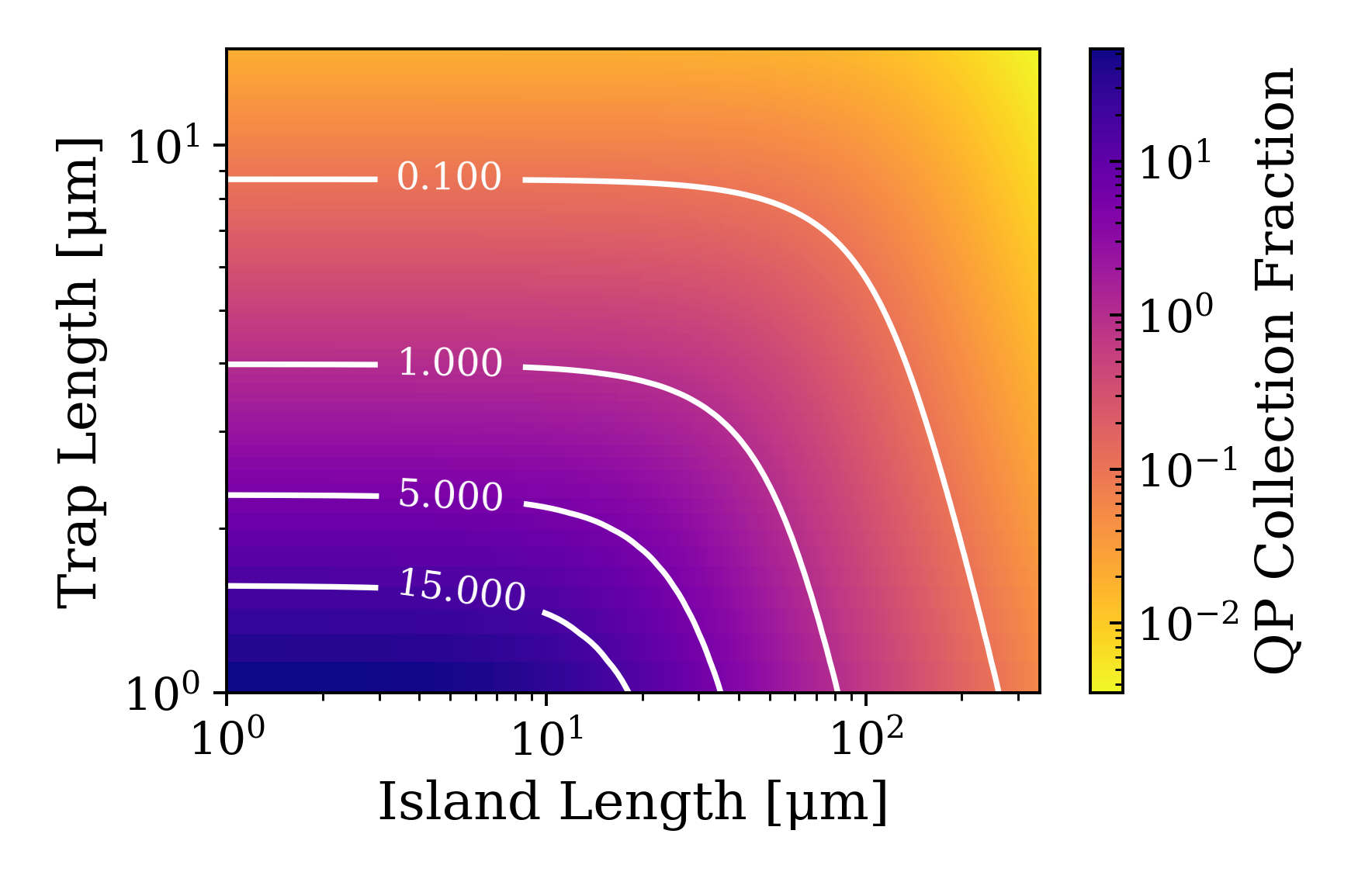
Quasiparticle Collection Efficiency—The coplanar capacitor islands in our device are designed to both maximize surface fill factor, and funnel QPs toward the junction. The funneling effect is achieved in part by the choice of a geometry that maximizes the QP collection efficiency for a given sensor area. We can achieve additional collection efficiency through the use of QP trapping [32, 33, 34], similar to that done with Quasiparticle-trap-assisted Electrothermal-feedback Transition-edge sensors (QETs) [35], by fabricating the islands with a material with a larger than the junction. For this proposed device, we choose Al for the athermal phonon collection region. For the trapping region and junctions, we require a material with a superconducting gap that is roughly a factor of 10 lower than Al. The simplest material to use would be AlMn (which we will assume for our calculations here), since its in thin films is easily tunable and it lends itself well to Josephson junction fabrication, as it naturally creates an aluminum oxide layer [36, 37, 38, 39].
The full quasiparticle diffusion model is described in detail in Appendix C, and we highlight the key features here. For a schematic diagram of the following, see Fig. 1.
-
1.
When a phonon or photon of energy greater than is absorbed by the island, a Cooper pair will be broken, and the resulting QPs will be promoted to well above the bandgap energy. These QPs will undergo a downconversion process to lower energy QPs and phonons, yielding a population of QPs at the band edge after [40]. During the downconversion process, a portion of the initial event energy will be lost as sub-gap phonons leak into the substrate [19]. For conventional S-wave superconducting films, incident events with energy will have approximately of the event energy remain in the QP system [41]. We will assume that the events will be in this energy regime and will adopt a value for the efficiency of the downconversion process ( of .
- 2.
-
3.
Once the QPs enter the lower- material they undergo a second downconversion process, resulting in an enhancement of QP number that scales with the ratio of the superconducting gaps of the two materials. These downconverted QPs have an energy lower than and become ‘trapped’. This multiplication process results in a signal enhancement, because the qubit is sensitive to QP number, not energy.
-
4.
While the QPs are trapped in the lower material, they will tunnel back and forth across the attached Josephson junction until recombination occurs. Each measured tunneling event results in a signal.
A plot of the QP collection fraction () as a function of QP trap and qubit island characteristic lengths, and respectively, for a square JJ can be seen in Fig. 2. Note that while this device adds an additional tunneling step beyond that of its QET counterpart [35], this efficiency loss can be made up by the addition of the QP multiplication and multiple tunnels – allowing for collection fractions that are greater than unity.
Qubit Tuning — In order to optimize the readout of these sensors, we must first tune the SQUAT design. Here, we focus on three main design parameters:
-
1.
The undressed resonance frequency, ;
-
2.
The maximum frequency separation of the even and odd parity states, ;
-
3.
The total quality factor of the qubit coupled to the feed line, ;
We model the qubits as notch filters, assuming an ideal transmision line, as [44],
| (9) |
where the qubit resonance frequency is a function of qubit charge and state spacing . Converting from Eq. 1 into frequency, we see that (in the transmon limit), is well approximated by the sinusoidal function
| (10) |
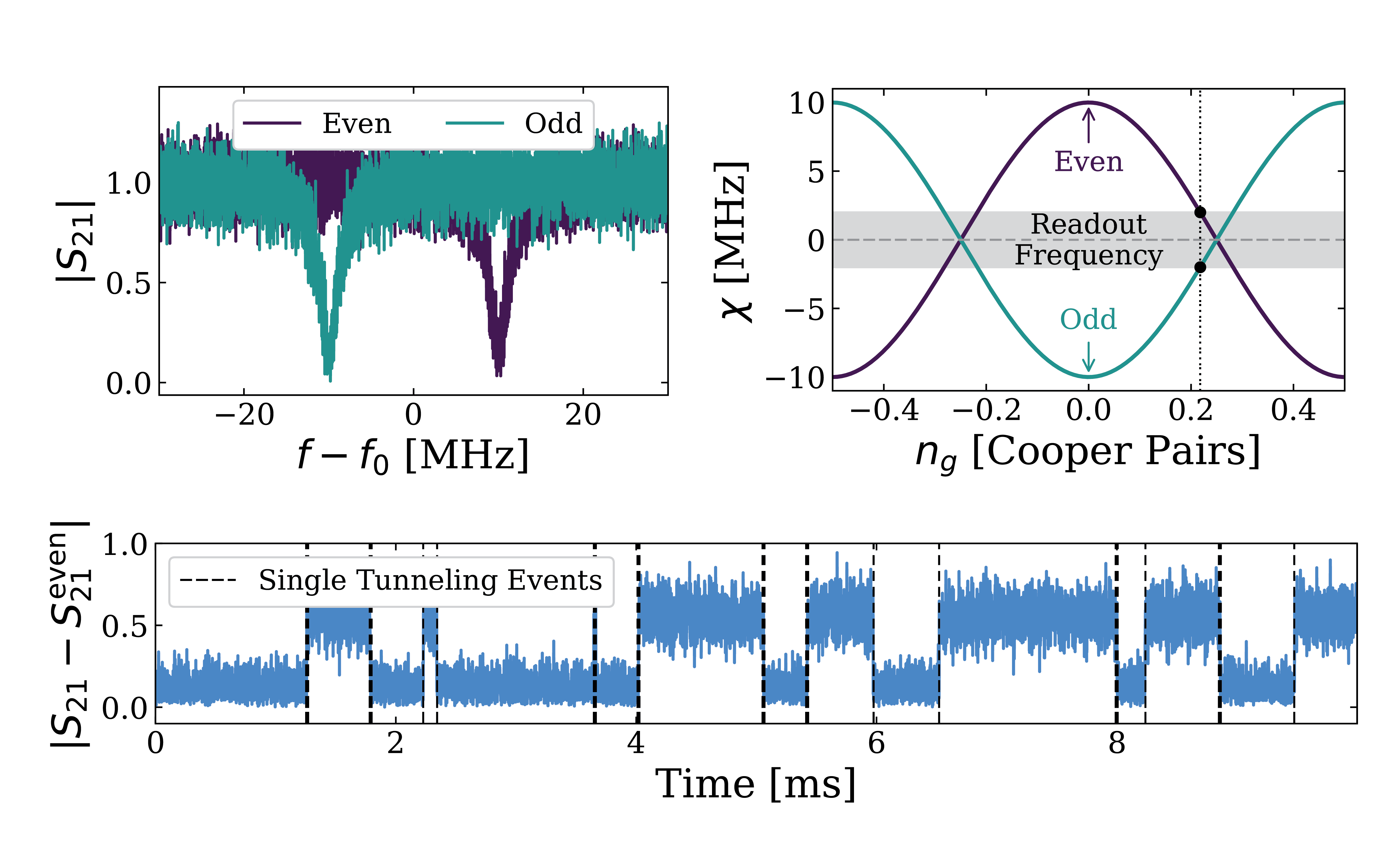
We can choose a charge operating point by applying a charge bias along the readout line or using a dedicated charge gate. Effectively this charge bias tunes the state frequency spacing, represented in Eq. 1 as . When a quasiparticle tunneling event imparts a fixed charge shift of 1 electron (shifting the overall phase by ) the magnitude of the shift of is a fraction of the maximum shift set by the operating point (see Fig. 3, right).
From Eqs. 2 and 3, we can see that and are both determined by and , and thus these parameters must be co-optimized. We first choose to be in the operating range of standard RF electronics, e.g. GHz (this is also informed by available quantum-limited readout). We must also assure that the state separation (determined solely by ) is in the weakly-charge sensitive limit, . Note that we will return to the precise optimization of in the next section.
With and chosen, we turn to the question of resonance bandwidth, which is given by . The sensors can be readily fabricated to have high-enough fidelity that the limiting quality factor is determined by that of the qubit-to-feedline coupling, . The optimal bandwidth depends on the readout method, as discussed later in this section and in Appendix A. In order to effectively resolve phonon events at the timescale of we must achieve a bandwidth of , implying .
Using simulations in HFSS we have demonstrated that generating designs within the optimal parameter space is easily achievable; an example of a SQUAT design tuned for phase readout is shown in Fig. 1a. The fact that an optimization is possible can be made intuitive by thinking about how each parameter depends on the geometry:
-
•
depends almost entirely on the capacitive coupling between the qubit and the feedline. So, tuning is achieved by changing the island-feedline separation.
-
•
is inversely dependent on the effective capacitance between the islands. Although the capacitance between the islands and the feedline contributes to this total, it is subdominant to the direct island-to-island capacitance.
-
•
depends on junction parameters including the junction area and thickness. Although the junction effectively acts as a parallel plate capacitor, this capacitance is also less than the direct island-to-island capacitance that dominates .
-
•
To choose , one can fix the ratio.
-
•
Then, with fixed ratio, and can be varied together to get an appropriate .
The optimal and are determined by the need to optimize readout signal-to-noise ratio (SNR).
In order to read out the SQUAT, a signal tone of fixed frequency is pumped through the feedline; we will discuss which frequency is optimal later. We will focus on a transmission measurement, although a reflection measurement is also possible in principle. Given an input readout tone , the signal is described by a complex voltage,
| (11) |
While we measure voltage directly, we convert the voltage signal to power and phase, which allows us to factor out impedance sources in our sensitivity calculations. The measured power transmitted is thus
| (12) |
with a phase shift of
| (13) |
where is the input tone power. This also allows us to determine the power dissipated in the device, with a precision determined by the degree to which attenuation and gain in our readout system are known.
There are two fundamental modes in which we can read out the SQUATs in this two-dimensional basis. The first mode is to observe a shift in the amplitude of the transmitted signal, with phase shift fixed at zero; the second is to observe a shift in the signal phase with amplitude unchanged. Both correspond to states separated by the diameter of the resonator circle in the IQ space, but amplitude readout is less sensitive to the precise frequency dispersion of the qubit, while properly-optimized phase readout is less sensitive to readout frequency. These cases are discussed in more detail in Appendix A, and summarized qualitatively here to focus on readout optimization results for the SQUAT.
In the amplitude readout mode, the optimal signal would be one in which equals 1 or 0 for the different parity states, so that the signal tone completely appears () or disappears () during a tunneling event. This situation can be achieved if the readout tone is within the bandwidth of one of the parity states and there is effectively no overlap of the two states, e.g. the state separation is much larger than the resonator width:
| (14) |
In the second readout mode, in which we wish to measure distance between states in the complex plane, a different optimization of and is necessary. Consider placing the readout tone at a frequency between the parity state frequencies, such that the transmitted magnitude is constant, but a relative phase shift is observed. As we derive in detail in Appendix A, the measured phase shift is maximized when
| (15) |
The main advantage of this second readout scheme is, as shown in the appendix, that a sensor optimized in this way will produce a fixed shift in the IQ plane for any readout frequency between the two parity states. This means we don’t need to worry about precise readout frequency optimization. In this case, in which noise is uncorrelated in phase, we will not see a large difference in readout fidelity as a function of readout frequency. For noise primarily in the phase or amplitude direction, we can adjust readout frequency to minimize the amount of noise projected onto our readout vector.
For both of these cases, we show in Appendix B that the qubit fidelity is just defined by the noise temperature and readout power according to the equation
| (16) |
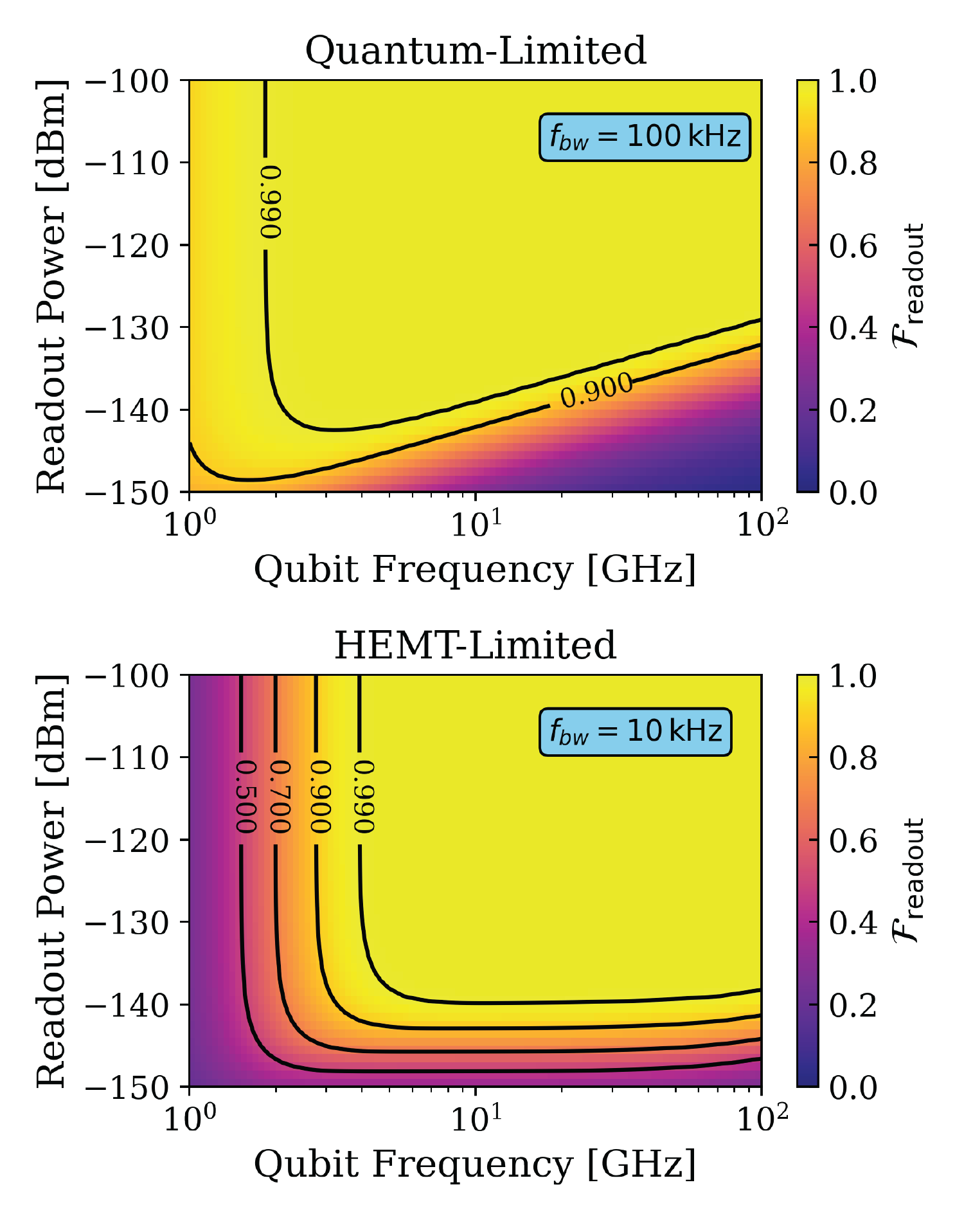
where is the readout bandwidth, is the system noise temperature, and is the readout frequency of the SQUAT. For 1.8 K and 6 GHz, Eq. 16 dictates that we can achieve high readout fidelity above -135 dBm readout power for an integration time corresponding to . With a quantum-limited readout, we find the reduced equation
| (17) |
where high fidelity is achieved above at Hz. These readout powers have already been used to demonstrate high readout fidelity for state-of-the-art qubits. Real devices will need to map out the tradeoffs between parasitic pair-breaking of the readout tone and noise-limited readout, and may benefit from stimulated emission from the SQUAT at higher readout powers.
In practice, the difference in SNR between phase and amplitude readout will be determined by the level of phase noise in the system (which we elaborate on in Appendix B.1), and will be assessed during first device tests. We have the freedom to tune state separation to optimize for either readout mode.
Estimated Sensor Performance—We can combine all of our known efficiency factors to predict the final energy sensitivity of the device to both direct absorption of photons and measurement of athermal phonons in the substrate. Recall that we are measuring total QP number , where is the total energy in the QP system. The energy in the QP system can be written as the product of the impinging particle energy (), the absorption efficiency () and the efficiency from the downconversion process (). Thus, our measured number of QP tunneling events () will be
| (18) |
where is the QP collection fraction given by Eq. 62, and is the efficiency of the particle absorption in the sensor, i.e. the antenna coupling for photons and the signal loss due to passive surfaces for phonons.
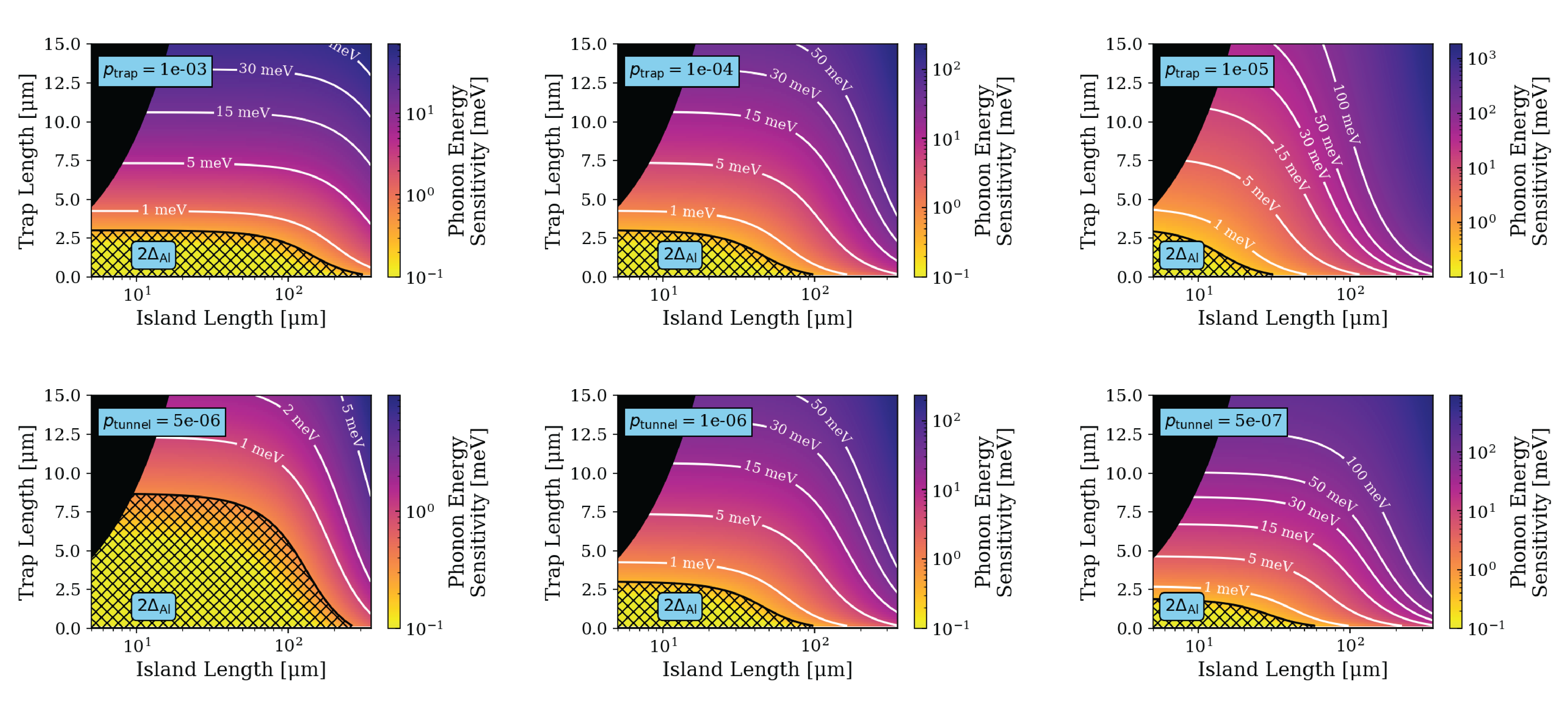
Considering first the athermal phonon detection, taking the worst case scenario that all the phonons are above the Nb gap, our phonon collection efficiency due to passive surface losses is roughly . Note that this value is relatively independent of individual sensor size, and the total sensor number can be changed to keep the surface coverage the same. Reading out the detector such that a single QPs can be counted, we calculate what the expected athermal phonon energy sensitivity threshold is of the entire detector, shown in Fig. 4. From the figure, we can see that for various geometries the SQUAT can easily achieve single meV phonon thresholds. They dynamic range of the measurement can span multiple order of magnitude in energy with minimal signal loss and is a function of of the measurement readout bandwidth, discussed in Appendix D.
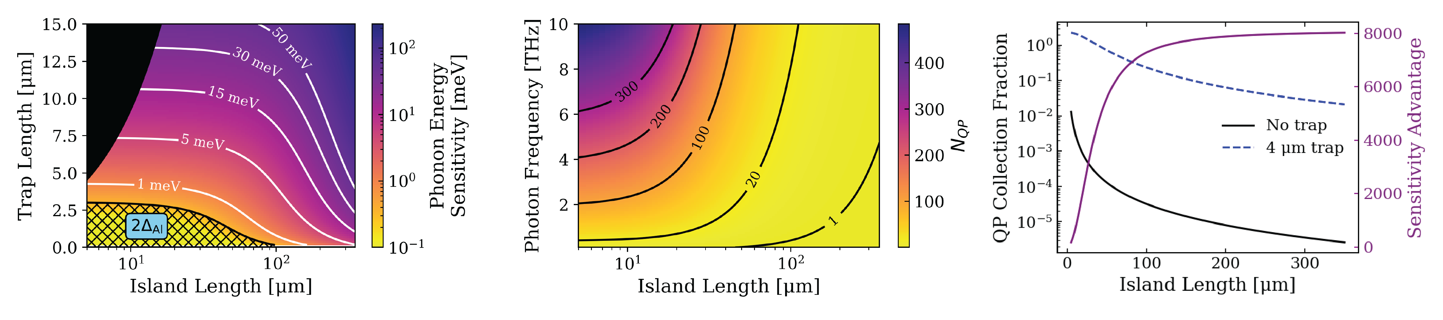
The photon energy sensitivity is expected to be similar to the phonon scenario since is very close for both cases. A full simulation of the antenna structure is left for future work, but from initial conservative estimates we expect that sensitivity to single sub-THz photons is reasonably achievable. A simulation of the expected sensor response as a function of photon energy and island length is shown in Fig. 4.
In order to illustrate the incredible gain in sensitivity that the QP trapping stage adds, we have plotted the simulated QP collection efficiency of the SQUAT sensor with a trap compared to an equivalent geometry sensor but without the trap in Fig. 4 right. As can be seen, the trapping region adds multiple orders of magnitude of phonon or photon sensitivity to the detectors.
Discussion—In this letter we have presented the design sketch and modeling of a novel detector concept based on superconducting qubit technology, which if properly optimized, would allow for sensitivities to particle interactions at the meV scale. While the majority of our quasiparticle model we have developed in Appendix C is based on previously measured data, we have made a few (conservative) assumptions, which we plan to measure in future work. Over the next few years, our R&D path towards realizing these devices is to:
-
•
Fabricate devices of the geometry presented in this paper using only Al for the islands and junctions (no QP trapping) to understand the optimization of the readout and qubit parameters.
-
•
Optimize the fabrication of separate AlMn (and similar materials) junctions to understand the QP tunneling probability of the junctions.
-
•
Fabricate the complete SQUAT sensor as described in this paper to measure the QP trapping probability at the Al/AlMn overlap.
With the AlMn trapping and tunneling parameters measured, a further optimization of the sensors will be possible. Once the sensitivity is maximized, the SQUATs have a large number of use cases, primarily in the low-energy, rare-event regime. The sensor offers two different pathways for event detection:
-
1.
The antenna structure of the sensor itself allows this device to be sensitive to single THz photons, allowing the devices to used in searches for QCD axion DM such as BREAD [45]. Additionally, this device is sensitive to electromagnetically-interacting fermionic light dark matter (LDM) via direct absorption or scattering in the island itself as proposed in [46].
-
2.
The incredible sensitivity to athermal phonons in the device makes it well-suited to detect LDM at the mass scale and sub-eV bosonic DM such as dark photons. Absorption of LDM and far-IR photons is possible in Si via a multiphonon excitation process [47, 48]. The LDM or photon coupling strength can be increased by using a polar crystal substrate [49, 50] or a low-bandgap semiconductor [51, 52]. In all of these cases, sensitivity to acoustic phonons at the scale is required.
While there already exists a large amount of competition in the space of superconducting sensors for low-energy rare-event measurement [53, 54, 55, 56, 57, 58, 59], the device we have proposed potentially offers multiple orders of magnitude of improvement in terms of absolute energy sensitivity beyond these currently existing detectors. Furthermore, because each qubit sensor is naturally read out individually, they inherently have a powerful background discrimination tool by determining the location in the detector in which the event occurred.
Acknowledgements—Thanks to Sasha Anferov for several useful conversations about qubit modeling. This work was supported in part by the US Department of Energy Early Career Research Program (ECRP) under FWP 100872. Caleb Fink is supported by the Laboratory Directed Research and Development program of Los Alamos National Laboratory. C. P. Salemi is supported by the Kavli Institute for Particle Astrophysics and Cosmology Porat Fellowship. This work was supported in part by the DOE Office of Science High Energy Physics QuantISED program.
References
- Vepsäläinen et al. [2020] A. P. Vepsäläinen, A. H. Karamlou, J. L. Orrell, A. S. Dogra, B. Loer, F. Vasconcelos, D. K. Kim, A. J. Melville, B. M. Niedzielski, J. L. Yoder, S. Gustavsson, J. A. Formaggio, B. A. VanDevender, and W. D. Oliver, Nature 584, 551 (2020).
- Wilen et al. [2021] C. D. Wilen, S. Abdullah, N. A. Kurinsky, C. Stanford, L. Cardani, G. D’Imperio, C. Tomei, L. Faoro, L. B. Ioffe, C. H. Liu, A. Opremcak, B. G. Christensen, J. L. DuBois, and R. McDermott, Nature 594, 369 (2021).
- McEwen et al. [2021] M. McEwen, L. Faoro, K. Arya, A. Dunsworth, T. Huang, S. Kim, B. Burkett, A. Fowler, F. Arute, J. C. Bardin, A. Bengtsson, A. Bilmes, B. B. Buckley, N. Bushnell, Z. Chen, et al., Nat. Phys. 18, 107 (2021).
- Martinis [2021] J. M. Martinis, npj Quantum Inf. 7, 90 (2021).
- Iaia et al. [2022] V. Iaia, J. Ku, A. Ballard, C. P. Larson, E. Yelton, C. H. Liu, S. Patel, R. McDermott, and B. L. T. Plourde, Nat. Commun. 13, 6425 (2022).
- Shaw et al. [2009] M. D. Shaw, J. Bueno, P. Day, C. M. Bradford, and P. M. Echternach, Phys. Rev. B 79, 144511 (2009).
- Echternach et al. [2018] P. M. Echternach, B. Pepper, T. J. Reck, and C. M. Bradford, Nat. Astron. 2, 90 (2018).
- Ristè et al. [2013] D. Ristè, C. C. Bultink, M. J. Tiggelman, R. N. Schouten, K. W. Lehnert, and L. DiCarlo, Nat. Commun. 4, 1913 (2013).
- Serniak et al. [2018] K. Serniak, M. Hays, G. de Lange, S. Diamond, S. Shankar, L. D. Burkhart, L. Frunzio, M. Houzet, and M. H. Devoret, Phys. Rev. Lett. 121, 157701 (2018).
- Mannila et al. [2021] E. T. Mannila, P. Samuelsson, S. Simbierowicz, J. T. Peltonen, V. Vesterinen, L. Grönberg, J. Hassel, V. F. Maisi, and J. P. Pekola, Nature Physics 18, 145 (2021).
- Kurter et al. [2022a] C. Kurter, C. Murray, R. Gordon, B. Wymore, M. Sandberg, R. Shelby, A. Eddins, V. Adiga, A. Finck, E. Rivera, A. Stabile, B. Trimm, B. Wacaser, K. Balakrishnan, A. Pyzyna, et al., npj Quantum Inf. 8, 31 (2022a).
- Koch et al. [2007] J. Koch, T. M. Yu, J. Gambetta, A. A. Houck, D. I. Schuster, J. Majer, A. Blais, M. H. Devoret, S. M. Girvin, and R. J. Schoelkopf, Phys. Rev. A 76, 042319 (2007).
- Barends et al. [2013] R. Barends, J. Kelly, A. Megrant, D. Sank, E. Jeffrey, Y. Chen, Y. Yin, B. Chiaro, J. Mutus, C. Neill, P. O’Malley, P. Roushan, J. Wenner, T. C. White, A. N. Cleland, and J. M. Martinis, Phys. Rev. Lett. 111, 080502 (2013).
- Wallraff et al. [2004] A. Wallraff, D. I. Schuster, A. Blais, L. Frunzio, R.-S. Huang, J. Majer, S. Kumar, S. M. Girvin, and R. J. Schoelkopf, Nature 431, 162 (2004).
- Kelly et al. [2015] J. Kelly, R. Barends, A. G. Fowler, A. Megrant, E. Jeffrey, T. C. White, D. Sank, J. Y. Mutus, B. Campbell, Y. Chen, Z. Chen, B. Chiaro, A. Dunsworth, I.-C. Hoi, C. Neill, et al., Nature 519, 66 (2015).
- Tosi, Vion, and le Sueur [2019] L. Tosi, D. Vion, and H. le Sueur, Phys. Rev. Appl. 11, 054072 (2019).
- Martinez et al. [2019] M. Martinez, L. Cardani, N. Casali, A. Cruciani, G. Pettinari, and M. Vignati, Phys. Rev. Appl. 11, 064025 (2019).
- Fink [2022] C. W. Fink, A Gram-Scale low-Tc Low-Surface-Coverage Athermal-Phonon Sensitive Dark Matter Detector, Ph.D. thesis, University of California, Berkeley (2022).
- Kaplan et al. [1976] S. B. Kaplan, C. C. Chi, D. N. Langenberg, J. J. Chang, S. Jafarey, and D. J. Scalapino, Phys. Rev. B 14, 4854 (1976).
- Pyle [2012] M. Pyle, Optimizing the design and analysis of cryogenic semiconductor dark matter detectors for maximum sensitivity, Ph.D. thesis, Stanford University (2012).
- Agnese et al. [2018] R. Agnese et al. (SuperCDMS Collaboration), Phys. Rev. Lett. 121, 051301 (2018), [Erratum: Phys. Rev. Lett. 122, 069901 (2019)].
- Smith et al. [2023] Z. J. Smith, C. Zhang, S. Henderson, Z. Ahmed, Y. Y. Chang, S. Gowala, K. Ramanathan, A. Simchony, O. Wen, B. A. Young, and N. A. Kurinsky, in LTD20 (Daejeon, South Korea, 2023).
- Rosenberg et al. [2017] D. Rosenberg, D. Kim, R. Das, D. Yost, S. Gustavsson, D. Hover, P. Krantz, A. Melville, L. Racz, G. O. Samach, S. J. Weber, F. Yan, J. L. Yoder, A. J. Kerman, and W. D. Oliver, npj Quantum Information 3 (2017), 10.1038/s41534-017-0044-0.
- Ren, Lv, and Chang [2008] Y.-J. Ren, P. Lv, and K. Chang, in 2008 IEEE Antennas and Propagation Society International Symposium (2008) pp. 1–4.
- Apriono et al. [2018] C. Apriono, A. Aji, T. Wahyudi, F. Zulkifli, and E. Rahardjo, Int. J. Technol. 9, 589 (2018).
- Wahyudi et al. [2017] T. Wahyudi, C. Apriono, F. Zulkifli, and E. Rahardjo (2017) pp. 372–376.
- Carelli et al. [2017] P. Carelli, F. Chiarello, G. Torrioli, and M. G. Castellano, J. Infrared Millim. Terahertz Waves 38, 303 (2017).
- Mori, Igawa, and Kojima [2014] T. Mori, H. Igawa, and S. Kojima, in Materials Science and Engineering Conference Series, Vol. 54 (2014) p. 012006.
- Grbovic et al. [2011] D. Grbovic, F. Alves, B. Kearney, K. Apostolos, and G. Karunasiri, in SENSORS, 2011 IEEE (2011) pp. 172–175.
- Naftaly and Dudley [2011] M. Naftaly and R. Dudley, Appl. Opt. 50, 3201 (2011).
- Stutzman and Thiele [2012] W. L. Stutzman and G. A. Thiele, Antenna Theory and Design, 3rd ed. (John Wiley and Sons, Chichester, England, 2012).
- Booth [1987] N. E. Booth, Appl. Phys. Lett. 50, 293 (1987).
- Goldie et al. [1990] D. J. Goldie, N. E. Booth, C. Patel, and G. L. Salmon, Phys. Rev. Lett. 64, 954 (1990).
- Ullom, Fisher, and Nahum [1996] J. Ullom, P. Fisher, and M. Nahum, Nuclear Instruments and Methods in Physics Research Section A: Accelerators, Spectrometers, Detectors and Associated Equipment 370, 98 (1996), proceedings of the Sixth International Workshop on Low Temperature Detectors.
- Irwin et al. [1995] K. D. Irwin, S. W. Nam, B. Cabrera, B. Chugg, and B. A. Young, Rev. Sci. Instrum. 66, 5322 (1995).
- Deiker et al. [2004] S. W. Deiker, W. Doriese, G. C. Hilton, K. D. Irwin, W. H. Rippard, J. N. Ullom, L. R. Vale, S. T. Ruggiero, A. Williams, and B. A. Young, Appl. Phys. Lett. 85, 2137 (2004).
- ONeil et al. [2010] G. ONeil, D. Schmidt, N. Tomlin, and J. Ullom, J. Appl. Phys. 107, 093903 (2010).
- O’Neil et al. [2012] G. C. O’Neil, P. J. Lowell, J. M. Underwood, and J. N. Ullom, Phys. Rev. B 85, 134504 (2012).
- Li et al. [2016] D. Li, J. E. Austermann, J. A. Beall, D. T. Becker, S. M. Duff, P. A. Gallardo, S. W. Henderson, G. C. Hilton, S.-P. Ho, J. Hubmayr, B. J. Koopman, J. J. McMahon, F. Nati, M. D. Niemack, C. G. Pappas, et al., J. Low Temp. Phys. 184, 66 (2016).
- Kozorezov et al. [2000] A. G. Kozorezov, A. F. Volkov, J. K. Wigmore, A. Peacock, A. Poelaert, and R. den Hartog, Phys. Rev. B 61, 11807 (2000).
- Guruswamy, Goldie, and Withington [2014] T. Guruswamy, D. J. Goldie, and S. Withington, Supercond. Sci. Technol. 27, 055012 (2014).
- Gray, Long, and Adkins [1969] K. E. Gray, A. R. Long, and C. J. Adkins, Philos. Mag. 20, 273 (1969).
- de Visser et al. [2014] P. J. de Visser, D. J. Goldie, P. Diener, S. Withington, J. J. A. Baselmans, and T. M. Klapwijk, Phys. Rev. Lett. 112, 047004 (2014).
- Probst et al. [2015] S. Probst, F. B. Song, P. A. Bushev, A. V. Ustinov, and M. Weides, Rev. Sci. Instrum. 86, 024706 (2015).
- Liu et al. [2022] J. Liu, K. Dona, G. Hoshino, S. Knirck, N. Kurinsky, M. Malaker, D. W. Miller, A. Sonnenschein, M. H. Awida, P. S. Barry, K. K. Berggren, D. Bowring, G. Carosi, C. Chang, A. Chou, R. Khatiwada, S. Lewis, J. Li, S. W. Nam, O. Noroozian, and T. X. Zhou (BREAD Collaboration), Phys. Rev. Lett. 128, 131801 (2022).
- Das, Kurinsky, and Leane [2022] A. Das, N. Kurinsky, and R. K. Leane, “Dark matter induced power in quantum devices,” arXiv:2210.09313 [hep-ph] (2022).
- Ikezawa and Ishigame [1981] M. Ikezawa and M. Ishigame, J. Phys. Soc. Jpn. 50, 3734 (1981).
- Hochberg, Lin, and Zurek [2017] Y. Hochberg, T. Lin, and K. M. Zurek, Phys. Rev. D 95, 023013 (2017).
- Griffin et al. [2020] S. M. Griffin, K. Inzani, T. Trickle, Z. Zhang, and K. M. Zurek, Phys. Rev. D 101, 055004 (2020).
- Trickle et al. [2020] T. Trickle, Z. Zhang, K. M. Zurek, K. Inzani, and S. M. Griffin, J. High Energy Phys. 03, 036 (2020).
- Rosa et al. [2020] P. Rosa, Y. Xu, M. Rahn, J. Souza, S. Kushwaha, L. Veiga, A. Bombardi, S. Thomas, M. Janoschek, E. Bauer, et al., npj Quantum Mater. 5, 52 (2020).
- Piva et al. [2021] M. M. Piva, M. C. Rahn, S. M. Thomas, B. L. Scott, P. G. Pagliuso, J. D. Thompson, L. M. Schoop, F. Ronning, and P. F. S. Rosa, Chem. Mater. 33, 4122 (2021).
- Fink et al. [2020] C. W. Fink, S. L. Watkins, T. Aramaki, P. L. Brink, S. Ganjam, B. A. Hines, M. E. Huber, N. A. Kurinsky, R. Mahapatra, N. Mirabolfathi, W. A. Page, R. Partridge, M. Platt, M. Pyle, B. Sadoulet, et al., AIP Adv. 10, 085221 (2020).
- Miller et al. [2003] A. J. Miller, S. W. Nam, J. M. Martinis, and A. V. Sergienko, Appl. Phys. Lett. 83, 791 (2003).
- Karasik et al. [2012] B. S. Karasik, S. V. Pereverzev, A. Soibel, D. F. Santavicca, D. E. Prober, D. Olaya, and M. E. Gershenson, Appl. Phys. Lett. 101, 052601 (2012).
- Goldie et al. [2011] D. J. Goldie, A. V. Velichko, D. M. Glowacka, and S. Withington, J. Appl. Phys. 109, 084507 (2011).
- Lolli et al. [2013] L. Lolli, E. Taralli, C. Portesi, E. Monticone, and M. Rajteri, Appl. Phys. Lett. 103, 041107 (2013).
- Khosropanah et al. [2016] P. Khosropanah, T. Suzuki, M. L. Ridder, R. A. Hijmering, H. Akamatsu, L. Gottardi, J. van der Kuur, J. R. Gao, and B. D. Jackson, Proc. SPIE 9914, 99140B (2016).
- Fink et al. [2021] C. W. Fink, S. L. Watkins, T. Aramaki, P. L. Brink, J. Camilleri, X. Defay, S. Ganjam, Y. G. Kolomensky, R. Mahapatra, N. Mirabolfathi, W. A. Page, R. Partridge, M. Platt, M. Pyle, B. Sadoulet, et al. (CPD Collaboration), Appl. Phys. Lett. 118, 022601 (2021).
- Kurinsky [2018] N. A. Kurinsky, The Low-Mass Limit: Dark Matter Detectors with eV-Scale Energy Resolution, Ph.D. thesis, Stanford University (2018).
- Moffatt [2016] R. Moffatt, Two-Dimensional Spatial Imaging of Charge Transport in Germanium Crystals at Cryogenic Temperatures, Ph.D. thesis, Stanford University (2016).
- Barends et al. [2009] R. Barends, S. van Vliet, J. J. A. Baselmans, S. J. C. Yates, J. R. Gao, and T. M. Klapwijk, Phys. Rev. B 79, 020509 (2009).
- Sadleir et al. [2010] J. E. Sadleir, S. J. Smith, S. R. Bandler, J. A. Chervenak, and J. R. Clem, Phys. Rev. Lett. 104, 047003 (2010).
- Zhao et al. [2017] S. Zhao, D. J. Goldie, S. Withington, and C. N. Thomas, Superconductor Science and Technology 31, 015007 (2017).
- Yen [2015] J. J. Yen, Phonon Sensor Dynamics for Cryogenic Dark Matter Search Experiment, Ph.D. thesis, Stanford University (2015).
- Yen et al. [2016] J. J. Yen, J. M. Kreikebaum, B. Young, B. Cabrera, R. Moffatt, P. Redl, B. Shank, P. Brink, M. Cherry, and A. Tomada, J. Low Temp. Phys. 184, 30 (2016).
- Kurter et al. [2022b] C. Kurter, C. Murray, R. Gordon, B. Wymore, M. Sandberg, R. Shelby, A. Eddins, V. Adiga, A. Finck, E. Rivera, A. Stabile, B. Trimm, B. Wacaser, K. Balakrishnan, A. Pyzyna, et al., npj Quantum Information 8 (2022b), 10.1038/s41534-022-00542-2.
- ans [2023] “Ansys,” (2023).
Appendix A Resonator Readout Modes
When measuring the qubits, we can operate in two distinct modes: Amplitude and phase readout. Recall that our voltage signal is the transmission signal of a complex pulsed readout tone
| (19) |
Amplitude Readout—Since can only take on values between zero and one, it is clear to see that the maximum and minimum amplitudes that the signal voltage could ever take on would be and respectively. This is accomplished in practice by designing a state separation that is much larger than the bandwidth of the readout () such that one parity state is on resonance and the other state is outside the BW of the readout. This can be seen visually on the IQ circle in Fig. 5.
Phase Readout—The opposite readout technique would be to consider only the phase of the signal tone. The maximum phase separation between the two states occurs where the amplitude of the readout signal is the same, or rather
| (20) |
The optimization problem becomes finding the to maximize the phase separation between and . Let us first recall the definition of when limited by the quality factor of the coupling
| (21) |
where the qubit resonance frequency is given by
| (22) |
recalling that the effective dispersion .
For simplicity, let us write as
| (23) | ||||
| (24) |
where can be written for the even and odd states as
| (25) |
Separating into IQ space we get that
| (26) | ||||
| (27) |
and the phase angle is
| (28) |
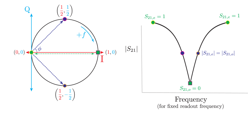
Considering two points on the IQ unit circle (see Fig. 5), the maximum separation (maximum signal) of phase between the points occurs when they are separated by a phase shift of . Since the signal is symmetric about the I axis, the maximum corresponds to .
| (29) | ||||
| (30) | ||||
| (31) | ||||
| (32) |
since . Finally, this gives us the optimum dispersion for a given bandwidth,
| (33) |
Appendix B Readout Fidelity
Given the readout modes described in Appendix A, we are prepared now to talk about readout fidelity for this type of sensor design. The readout in either case is a measurement of transmitted power across the resonator given a known input tone power and phase. Alternatively, we can frame the signal amplitude as the distance between even and odd parity states in IQ space. In the general case, the distance between two points in IQ space is
| (34) |
For the amplitude case, measured power transmitted through the qubit for an input power is
| (35) |
and for phase readout, where the signal is constant in I and only the sign of Q changes, we find
| (36) |
Thus in terms of signal amplitude, there’s no difference between these readout modalities.
Let’s now consider the general case for the optimization of the phase readout (in which we assume that we have access to both the phase and amplitude of ). Our optimization ensures that the even and odd states lie opposite each other on the resonance circle. For a rotation angle of about the point (I,Q) = (1/2,0), we find that
| (37) | ||||
| (38) |
where for the even/odd state. We thus find that
| (39) | ||||
| (40) | ||||
| (41) | ||||
| (42) |
which tells us that for the general case of a frequency shift from the optimal readout frequency, for an optimized design,
| (43) | ||||
| (44) |
Thus the design optimized for phase readout will have the same signal amplitude regardless of the readout frequency, as the two points will be shifted an equal amount around the resonator circle but maintain unit distance between them. Contrast this with amplitude readout in the non-optimized case, where maximum signal is only achieved when the readout frequency is exactly the frequency of one of the parity states.
One important caveat to this argument is that, unlike a lumped-element resonator, the SQUAT cannot interact with more than one photon at a time. We can account for this by adding a readout efficiency term to the signal part of our sensitivity calculation, which accounts for the photons that are unable to interact with the SQUAT after the initial photon has been absorbed. This efficiency is given by the equation
| (45) |
The frequency dependence comes both from calculating the decay rate for a given coupling factor and from converting readout power into photon number, leading to the conclusion that SQUAT efficiency improves for lower Q or higher readout frequency. This also shows that for high readout power we suffer from the limited number of photons interacting with the SQUAT.
Having established that our signal amplitude is always equal to our readout power, we now consider the noise contribution to our signal in order to determine readout fidelity. Assuming we are limited by Johnson-Nyquist noise (which is uncorrelated to the signal), we find a noise power in an impedance matched network of
| (46) |
where
| (47) |
is the readout bandwidth of the measurement, and is the physical temperature of the system. The role of is to introduce quantum corrections from vacuum fluctuations that break the strict temperature dependence of the noise; for low-enough physical system temperature, this is reduced to the simpler, quantum-limited expression
| (48) |
If we assume that the noise and signal are uncorrelated, we can continue to use readout power as our signal to write down the signal-to-noise ratio, or equivalently the inverse normalized signal variance, as
| (49) |
Here the factor of 2 comes from the fact that we have defined our signal as a difference; we thus need two measurements to establish that difference, and we pick up two noise contributions as a result. Note that given our signal in this case is a difference, the power noise can thus can be treated as a variance; this is different from an absolute measurement where noise power is a strictly positive number. As discussed in the main body of the paper, correlated noise such as TLS noise will modify the SNR, effectively by making the noise level dependent on the operating point on the IQ circle.
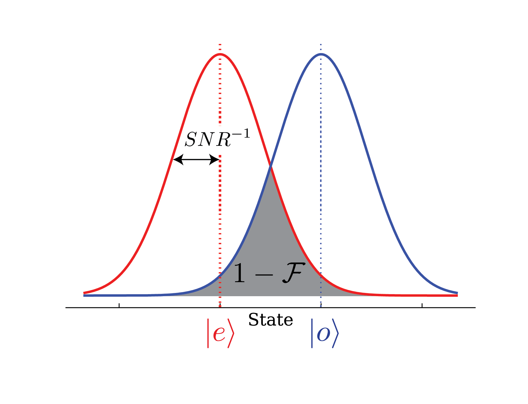
We can now consider the fidelity for our readout. Assuming random non-stationary noise, we can calculate the fidelity utilizing the square root of the overlap of two normal distributions (see Fig. 6) with and variance defined in Eq. 49,
| (50) |
This fidelity measure is the joint probability that the two states overlap, and goes to zero for low SNR, 1 for high SNR. Repeated readouts increase SNR, and thus in general, reduced readout bandwidth can be used to increase fidelity. A plot of the readout fidelity as a function of readout power and qubit resonance frequency for both a quantum limited and HEMT limited readout can be seen in Fig. 7.
B.1 Sources of Phase Noise
In the main body of the text and in this appendix (Appendix B), we have assumed the ideal case of perfect qubit stability and stationary, uncorrelated noise additive with I and Q. In reality, there are two major noise sources we have to worry about: charge noise and two-level system (TLS) noise. Charge noise affects the point on the dispersion curve and thus the state separation (we can think of this as a differential-mode phase noise). TLS noise affects the mean frequency of the device; it can be thought of as a common-mode phase noise.
In the case of charge noise, we can use the gate capacitance to estimate the effect of a known gate voltage noise on the system; TLS noise will be determined by the occupation and coupling of oxide states near the qubit to the qubit islands.
Appendix C Quasiparticle Diffusion Model
This diffusion model describes the dynamics of a non-equilibrium quasiparticle population in the qubit islands and how they are measured. As described in the text above, this quasiparticle population arises from an impinging particle, e.g. a phonon or photon, with energy greater than twice the superconducting bandgap of the island. The incident particle breaks a Cooper-pair into highly energetic quasiparticles, which then undergo a downconversion process into phonons and lower energy quasiparticles until a quasi-stable population of quasiparticles exists at the superconducting band edge [19]. A schematic diagram of the full process can be seen in Fig. 1.
C.1 QP Diffusion in Island
Similar to what is done in [18, 60], we model the QP transport in the island using a 2D diffusion model. We start with the diffusion equation
| (51) |
where is the QP number density, and are the diffusion coefficient and finite QP lifetime in the island (Al in this case), and is a source of particles. This differential equation can be solved in two dimensions; from [61], the fraction of QPs that get trapped in the overlapping region is given by
| (52) |
where and are modified Bessel functions of the first and second kind and
| (53) |
and are the effective radii of the island/trapping regions, and and are two competing length scales: the diffusion length and absorption length, given by
| (54) | |||
| (55) |
where is a film specific scalar for the case that the diffusion length is limited by the film thickness, is the island thickness, is the length of the overlapping region between the two materials, we refer to as the effective QP absorption velocity, and is the per QP transmission probability at the interface.
We must estimate , which is a function of the island material, the trapping material, and the thickness of the trap. For this model, we propose to use AlMn for the trap and junction - since its can be tuned with the amount of Mn added and AlOx layers can easily be formed on it to create junctions [38]. For the simplest model of QP trapping, we model the change in energy between the Al and AlMn trap as a step function between and . In reality, this step function will be slightly smeared by the proximity effect. We assume that the QPs that enter the trap are all at energy (since the QP downconversion timescale is orders of magnitude faster than the average time for a QP to reach the trap). The question then becomes: what is the probability that the QP undergoes a scattering process and loses enough energy such that it cannot travel back into the Al island? We are targeting a for the AlMn of roughly 10 times less than that of the Al islands. The QP scattering lifetime was measured in AlMn by [37] to be . Additionally, in [62] it was shown that increasing the disorder of Al films by adding Mn decreased the Al QP lifetime. Thus depending on the percent of Mn added, this scattering time could be even smaller.
Regarding the validity of the step-function model of the Al/AlMn interface, there are two factors that we must consider. The overlapping regions between the Island and the trap will have a global shift from the proximity effect in the Z direction, and the boundary of the overlapping region in the XY plane will have a local gradient from the longitudinal proximity effect [63]. While the proximity effect in AlMn has not been well studied, at least for Al in the dirty limit the coherence length has been measured [64] to be on the order of , which is a reasonable order of magnitude estimate for AlMn. Since our films for both the Island and trap will be thick, we expect this region to fully proximitized and we do not need to consider any spacial variation in the Z direction. Further, given the QP scattering time for AlMn, this is equivalent to . Thus for our initial designs with , we have the situation where
| (56) |
For both of these reasons, the trapping interface can be well approximated as a step function.
The scattering rate can be used to estimate the trapping probability for a given trap thickness from Eq. 7, repeated below for completeness,
| (57) |
where is the sound speed in the trap, is the thickness and is the QP-phonon scattering rate. Using a trap thickness of and scattering rate of from [37], the trapping probability for our Al/AlMn devices should be . It is interesting to note that this value is very close to that measured by [65, 66], who found that the trapping probability for Al/W traps is . For this model we will thus take the conservative approach and use in our calculations.
C.2 Quasiparticle Multiplication
When the quasiparticles enter the trap they will have energy of roughly (see Fig. 4 b). Once in the lower trap however, these QPs will undergo a downconversion step into a lower energy QP population. While some portion of the energy is lost to sub-gap phonons, there is ultimately a QP number enhancement given roughly by [32]
| (58) |
C.3 Quasiparticle Diffusion in Trap
At this point, a stable population of QPs has developed in the trap. We then model the trap QP transport using a 1D diffusion model, which is justified in this case since the length of this region is much larger than the width or film thickness. Solving Eq. 51 in one dimension, the fraction of QPs tunneling across the junction is given by
| (59) |
where is a scalar quantifying the diffusion in the thin film thickness limited case, and is the per-QP tunneling probability at the junction. Since the relative amount of Mn in the AlMn should be very low, the QP scattering diffusion length should be close to that of a typical Al thin film. As such, we use a value of as measured in [66]. From [67] we estimate the QP tunneling probability to be for pure Al. For the AlMn in this model, we adopt the conservative lower bound of .
This step is where the true utility of this design comes into fruition. While the QP tunneling probability across the Josephson junction is very small - requiring a QP on average to impinge upon the junction times on average before it tunnels, this setback is counteracted by confining the QP’s to a volume that is at least 5 orders of magnitude smaller than the islands.
C.4 Signal Gain from Multiple Tunneling Events
Since there is no potential difference across the junction, QPs near the junction will have multiple chances to tunnel before recombining. Using simple geometric arguments, we estimate the characteristic time it takes a QP in the trap to reach the junction as
| (60) |
where is the volume of the trap and is the length of a single side of the square Josephson junction, and is the QP velocity at the operating temperature. We can then define the average number of tunnels per-QP as
| (61) |
where is the QP lifetime in the junction material. While this term depends on many material parameters, it is reasonable to expect each QP will be measured times for an sized trapping region. However, since this effect needs to be studied, for this current model we make the conservative assumption that .
C.5 Total Quasiparticle Collection Efficiency
The final fraction of collected QPs starting with a stable QP population in the island is thus given by the product of Eqs. [52] [58] [59] [61]
| (62) |
And example plot of how this collection fraction depends on the model parameters is shown in Fig. 2 for the parameters given in the main text. Fig. 8 shows how the final energy resolution depends on the trapping and tunneling probabilities.
Appendix D Sensor Bandwidth
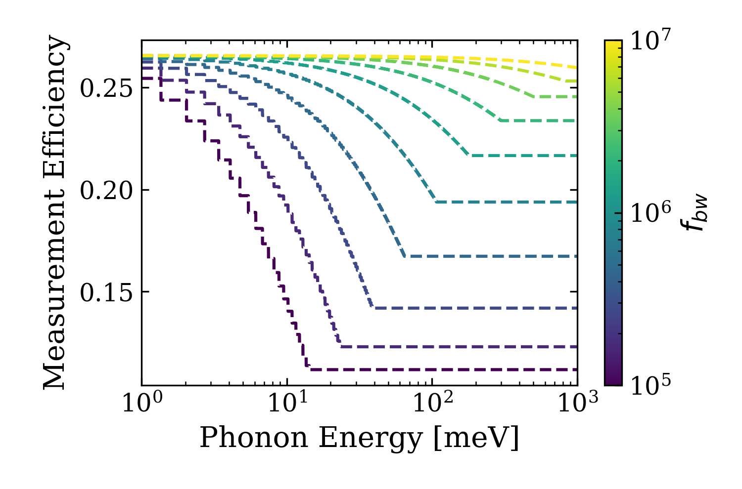
The energy measurement efficiency of the SQUAT will be ultimately limited by the total sensor bandwidth. For the case of direct photon absorption, there are two relevant timescales that need to be considered: the inverse readout bandwidth , and the average time between quasiparticle tunneling events . While the bandwidth is fixed, we note that the average tunneling time is energy dependent. For the case of phonon absorption there is an additional time constant of the average phonon collection time as given by Eq. 6.
We consider first the average time per quasiparticle tunnel. While this is technically a two stage process, the QPs must travel through the island before getting trapped and then must tunnel across the junction, the trapping time is at least four orders of magnitude faster than the tunneling time. As such, since the process is Poissonian, we can model the sensor response to an impulse of energy with a single pole exponential with a time constant set by . For a single quasiparticle in the trap, the characteristic time that it will take to diffuse to the trap is given by Eq. 60. The average time between tunneling events () will scale with both the total number of QPs and the average number of tunnels per QP , as
| (63) | ||||
| (64) |
Since the total number of quasiparticles is a function of the deposited energy, as given by Eq. 18, this means that the average time between tunneling events must also be energy dependent. We thus get that the fraction of quasiparticles in the trap that tunnel across the junction per unit time is described by
| (65) |
In the limit of infinite readout bandwidth, the fraction of measured tunneling events would be equal to the fraction of quasiparticles created. However, the SQUAT has a finite readout bandwidth; in our current design . In the worst case scenario, the consequence of this is that any consecutive tunneling events occurring in a shorter time interval than will not be accurately measured and we will get on average a measurement rate of . In this case we get that the fraction of measured QPs is
| (66) |
| (67) |
The above expression describes the response of the sensor to a direct energy absorption into the island, e.g. from a photon, and a plot of the measurement efficiency (taking into account the total quasiparticle efficiency model described in App. C) versus particle energy can be seen in Fig. 9. For the case of phonon absorption, we must take also into account the pulse shape of the phonon energy. The fraction of QP’s tunneling across the junction is now given by the convolution of Eq. 65 and Eq. 6. In this case we get that the total fraction of measured quasiparticles is given by
| (68) |
where
| (69) | ||||
| (70) | ||||
| (71) | ||||
| (72) | ||||
| . | (73) | |||
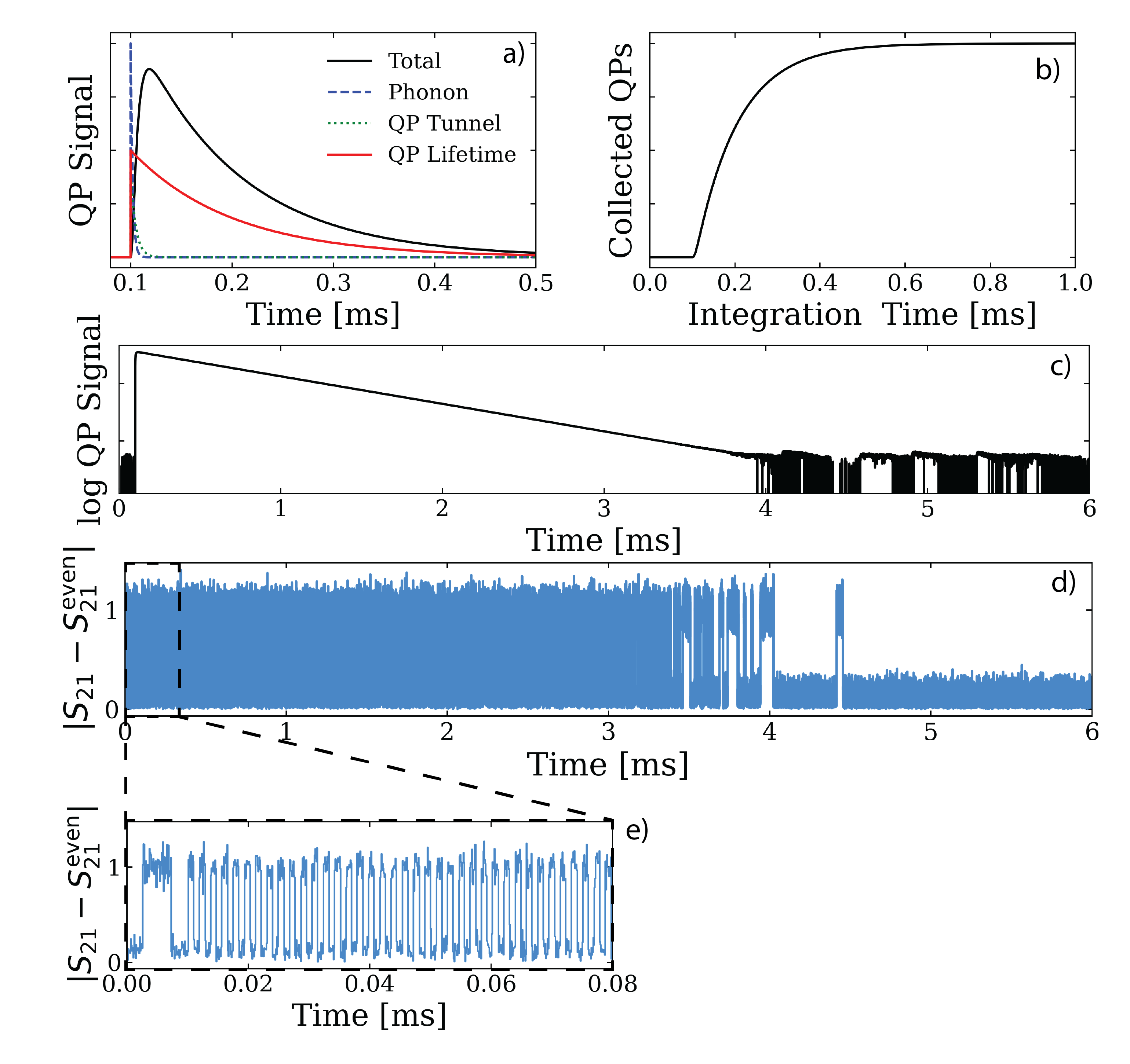
From Fig. 9 we can see that in the case that the phonon pulse is slower than the tunneling time and inverse readout bandwidth, the SQUAT readout efficiency will saturate. A simulated typical phonon pulse is shown in Fig. 10 as well as a depiction of what the measurement will physically look like in terms of the tunneling rate observed by the sensor.
Appendix E SQUAT geometric tuning and simulation
To achieve the optimal device parameters for a given readout method (as detailed in Appendix B), we must tune the geometry of the qubit and its coupling to the feedline. In this appendix we show how tuning various geometric parameters affects the readout parameters as simulated with ANSYS HFSS, a finite element RF modeling software [68].
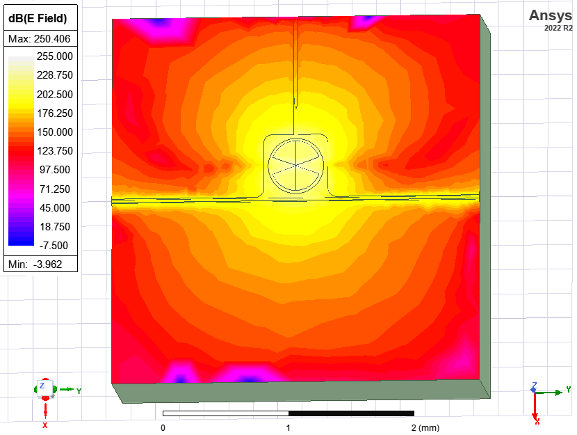
Each qubit is measured with a modal network simulation type. Just as the SQUATs will be in actual measurements, they are stimulated with a transmission measurement along the feedline. This is achieved in simulation with ports that inject modes at swept frequencies across the qubit resonance. An example electric field plot for a qubit driven on resonance is shown in Fig. 11.
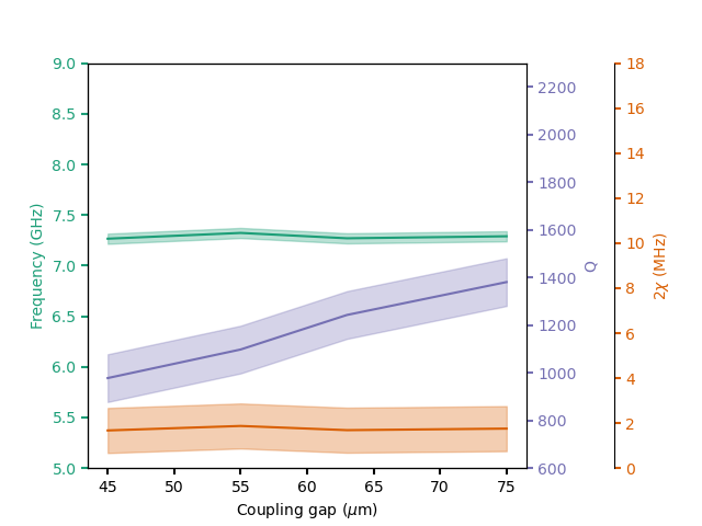
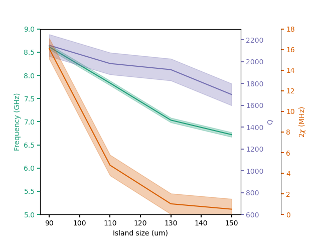
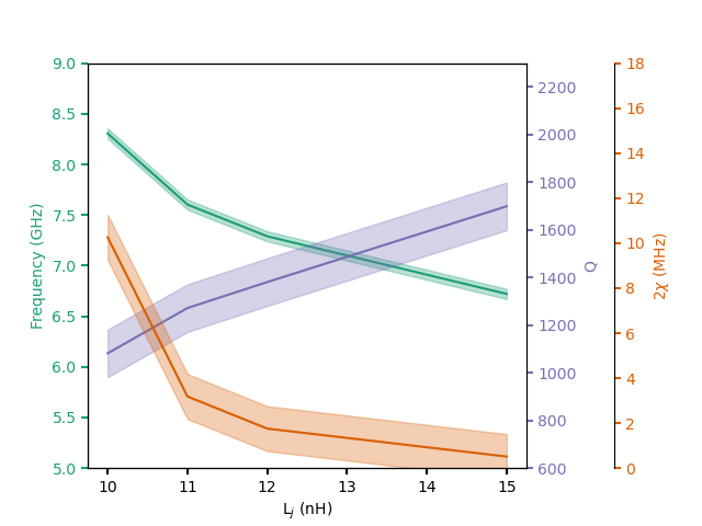
The trends in frequency, quality factor, and charge dispersion resulting from the HFSS simulations are shown in Fig. 12. The uncertainties shown there reflect how much variation in those parameters we expect based on a single simulation method, and do not include systematic uncertainties associated with differences between simulation and the real device. We expect the frequencies and quality factors to be fairly accurate, but the dispersion’s exponential dependence on (see Eq. 3) means that small discrepancies in the simulated versus actual and can lead to large differences in .
To see the magnitude of this effect, we ran an ANSYS Maxwell simulation to get another estimate for for some of the data points shown in the plots. The difference in was up to a factor of , leading to shifts of by up to two orders of magnitude. However, although the two simulation methods give different results, the overall dispersion trends with geometry should be consistent between the methods. Thus the curves in Fig. 12 should be interpreted for the geometric trends rather than for the values themselves. Once devices have been fabricated and tested, we will benchmark our simulations to the measured values.