Neural Lithography: Close the Design-to-Manufacturing Gap in Computational Optics with a ’Real2Sim’ Learned Photolithography Simulator
Abstract.
We introduce neural lithography to address the ‘design-to-manufacturing’ gap in computational optics. Computational optics with large design degrees of freedom enable advanced functionalities and performance beyond traditional optics. However, the existing design approaches often overlook the numerical modeling of the manufacturing process, which can result in significant performance deviation between the design and the fabricated optics. To bridge this gap, we, for the first time, propose a fully differentiable design framework that integrates a pre-trained photolithography simulator into the model-based optical design loop. Leveraging a blend of physics-informed modeling and data-driven training using experimentally collected datasets, our photolithography simulator serves as a regularizer on fabrication feasibility during design, compensating for structure discrepancies introduced in the lithography process. We demonstrate the effectiveness of our approach through two typical tasks in computational optics, where we design and fabricate a holographic optical element (HOE) and a multi-level diffractive lens (MDL) using a two-photon lithography system, showcasing improved optical performance on the task-specific metrics. The source code for this work is available on the project page: https://neural-litho.github.io.
1. Introduction
In recent years, we have witnessed a revolution in the design of computational optical elements, extending well beyond conventional lenses and mirrors. Holographic optical elements, as a representative example, have found applications in various domains, including 3D imaging as speckle generators [Intel, 2023], augmented reality as waveguide combiners [Jang et al., 2020, 2022], laser scanning as beam splitters [Hahn et al., 2020], and others [Kuo et al., 2020; Blachowicz et al., 2021]. Recent advances in deep learning and auto-differentiation [Baydin et al., 2018] have further enabled the development of end-to-end design pipelines for diffractive- [Sitzmann et al., 2018] and meta-optical [Tseng et al., 2021] imaging systems, demonstrating promising results in numerous imaging tasks, such as depth from defocus [Ikoma et al., 2021], hyperspectral imaging [Baek et al., 2021], high-dynamic-range imaging [Metzler et al., 2020; Sun et al., 2020a], and image pixel super-resolution [Sitzmann et al., 2018; Sun et al., 2020b]. These computational imaging devices facilitate the creation of compact, miniaturized, and multifunctional imaging devices and expand the capabilities of conventional vision systems, offering unprecedented opportunities to meet diverse imaging requirements.
Nonetheless, a crucial challenge remains: fabricating elements that fulfill design objectives, offering large design degrees of freedom (DOF), and being cost-effective. Present popular fabrication techniques include e-beam lithography [Tseng et al., 2021], diamond tuning [Sitzmann et al., 2018], and photolithography [Levin et al., 2013; Tan et al., 2021; Boominathan et al., 2020; Orange-Kedem et al., 2021; Baek et al., 2021] . Among these techniques, photolithography, which is the focus of this work, uniquely allows 3D manufacturing capacity [Blachowicz et al., 2021; You et al., 2020], exhibits low cost, easy prototyping, and allows larger and flexible design space [Lee et al., 2023], which are more or less unmet in other fabrication methods. Yet, a critical step, the numerical modeling of the photolithography process in the design loop, is often overlooked in previous studies [Jang et al., 2020; Tan et al., 2021; Boominathan et al., 2020].
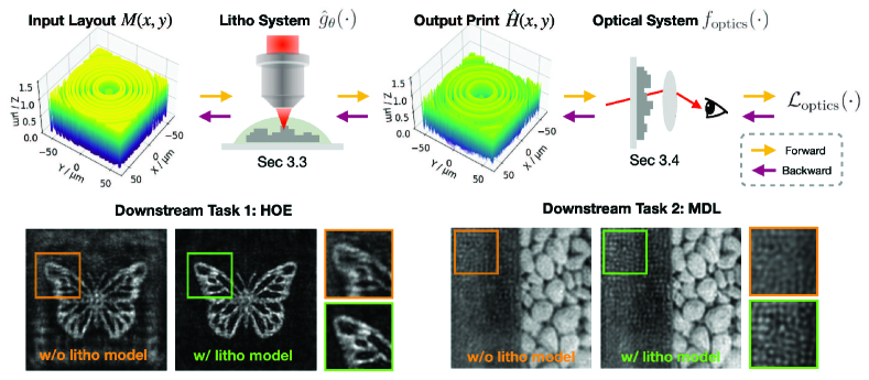
We identify this deficiency, a phenomenon we term the ”design-to-manufacturing gap” in computational optics, as a fundamental issue in the current design and fabrication process. This gap, arising from differences between the theoretical and actual outputs of the lithography system due to light diffraction and photo-chemical processes, has significant implications [Wang et al., 2020; Roques-Carmes et al., 2022]. This impairs not only the accuracy of optical information processing, the diffraction efficiency [Ikoma et al., 2021; Baek et al., 2021] but also the minimum controllable feature size, which is a critical parameter in computational optics as it determines the maximum diffraction angle [Levin et al., 2013] and the étendue of the optical system [Kuo et al., 2020]. While an intuitive solution is to numerically incorporate the manufacturability during the task design process, developing a high-fidelity simulator to ensure flawless integration and efficiently co-optimizing the task-specific design process remains a further challenge.
In response to these challenges, we propose a framework that integrates a pre-trained neural lithography simulator into the model-based optical design process to collectively work with the task-related computational optics models to let the design meet task-specific metrics while maintaining fabrication feasibility. This simulator, trained from the dataset explored in a real-world lithography system using a synergistic blend of traditional physics-based and data-driven modeling, compensates for the deviation between the ideal and the real lithography process. In this way, our framework mitigates the ”design-to-manufacturing gap” and enhances the fabrication fidelity of the design, leading to superior performance in downstream computational optical tasks.
Specifically, our contributions are:
-
•
A ”real2sim” methodology that learns high-fidelity neural simulators that accurately model real-world photolithography systems from 2.5D atomic force microscope (AFM) measurements.
-
•
A design and fabrication co-optimization pipeline that models the downstream computational optics task and photolithography process as two intersected differentiable simulators to optimize for desired optical performance post-manufacturing, using inline holography and imaging as example tasks.
-
•
Experimental verification of improved optical performance by fabricating optimized diffractive optical elements with a two-photon lithography (TPL) system and evaluating on a home-built optical setup.
Scope
This research employs a ’Real2Sim’ learning approach to construct high-fidelity neural photolithography simulators, specifically validated on TPL systems using AFM datasets. We take initial steps in the broad domain of co-optimizing manufacturability with computational optics design. We believe that the insights provided by our work are invaluable and could inspire further research in the fields of computational optics and photolithography.
2. Related work
Model-based optical proximity correction (OPC) and inverse lithography technology (ILT) are computational lithography techniques commonly used to compensate for errors due to diffraction or process effects during or after fabrication. Both methods are based on a simulator of the lithography system. The former refers to the solution of perturbing surrounding pixels of input design geometry through feedback from the simulator. The latter formulates the lithography enhancement task as an inverse design problem and sets the input design geometry as the targets with no limitation on the design DOF [Cecil et al., 2022]. Early research built a physics-based simulator of the lithography system and solved the ILT problem with adjoint methods/gradient descent/backpropagation [Cecil et al., 2022; Poonawala and Milanfar, 2007]. Recently, researchers have been using deep learning methods, such as LithoGAN [Ye et al., 2019], GAN-OPC [Yang et al., 2018], and optics-inspired neural networks [Yang et al., 2022b, a], neural-ILT [Jiang et al., 2020] to speed up the OPC or ILT process through learning a fast proxy from expensive simulated data generated from the physics-based simulator.
Our work addresses a critical challenge in computational lithography: constructing a high-fidelity digital twin of real-world lithography systems. Such systems have been modeled in a white-box manner, building physics-based simulators approximated from first principles in optics and photochemistry, like the Hopkins diffraction model for Kohler illumination and sigmoid functions for resist photochemical reactions [Cobb et al., 1996; Poonawala and Milanfar, 2007; Chevalier et al., 2021]. However, they fall short in adapting to system-specific and photoresist-specific variations [Arthur and Martin, 1996]. These limitations are not fully remedied even for industry standards like Sentaurus Lithography, which has evolved to simulate 3D resist profiles [Synopsys, 2023].
Against this backdrop, our research, while rooted in a learned representation of the lithography system, introduces a paradigm-shifting contribution that may significantly improve lithography performance. We employ a ’real2sim’ methodology 111real2sim is an emerging concept in robotics which advocates for building high-fidelity simulators directly from real-world data [ICRA, 2023]. for training our differentiable simulator from real 2.5D layout-print pairs, in contrast with the conventional ’sim2sim’ method. Therefore, our method offers a more adaptable and accurate way to digitalize the photolithography system while de-emphasizing the computational speed. Furthermore, our focus on 3D structures necessitates a more informative dataset – a ’2.5D’ heightmap of prints instead of ’2D’ datasets for common edge position error (EPE) corrections [Cecil et al., 2022].
Optimization of photolithography for micro/nano optics has seen recent advancements (Table 1). Wang et al. utilized grid search for Dammann gratings fabrication [Wang et al., 2020], while Lang et al. implemented a parameterized physics model for multi-photon lithography [Lang et al., 2022]. Chevalier et al. integrated a physics-based lithography model to optimize microlens array fabrication using atomic force microscopy data [Chevalier et al., 2021; Giessibl, 2003]. Of particular relevance is Liao et al.’s work [Liao et al., 2022], which leveraged machine learning to construct an i-line lithography simulator from real 2D binary scanning electron microscopy (SEM) data, leading to a non-differentiable OPC to optimize for the EPE. However, this process presents computational challenges, and the limited SEM dataset information hinders complex design capabilities.
| [Wang et al., 2020] | [Chevalier et al., 2021] | [Lang et al., 2022] | [Liao et al., 2022] | Ours | |
|---|---|---|---|---|---|
| Data-driven | (✓) | ✗ | ✓ | ✓ | ✓ |
| Physics | (✓) | ✓ | ✓ | (✓) | ✓ |
| 2.5D | ✓ | ✓ | ✓ | ✗ | ✓ |
| Nanoscale | ✓ | ✓ | ✗ | ✓ | ✓ |
| End-to-end | ✗ | ✗ | ✗ | ✗ | ✓ |
In contrast, our work employs a dataset measured by AFM, enabling optimization for geometry of computational optics. Furthermore, our approach is fully differentiable, combining optical design and fabrication correction end-to-end. By incorporating fabrication constraints directly in the design loop, this methodology navigates complex design space more effectively.
Differentiable optics refers to an emerging technique in computational optics that models an optical system with chained differentiable functions to design optical systems using gradient-based optimization methods, which is computationally efficient and effective in exploring large and complex design space. Recently, based on differentiable optics, a large body of work in computational imaging has studied the joint design of the optics and the reconstruction algorithms [Sitzmann et al., 2018; Tseng et al., 2021] using the physics-based (white-box) simulators.

Our neural/differentiable lithography also lies in the regime of differentiable optics. The uniqueness is that our work is the first to integrate design and manufacturing as two differentiable modules of an end-to-end optimization pipeline for high-performance computational optics tasks (Fig. 2). We, on the one hand, utilize the differentiable optics-based first principle to enable the optical design and, on the other hand, build a differentiable neural lithography simulator in a ’real2sim’ manner (the gray-box simulator) for the lithography process. The latter resembles very recent work on ’hardware-in-the-loop’ optimization of camera ISP [Tseng et al., 2019] and holographic display system [Peng et al., 2020; Chakravarthula et al., 2020].
3. Methodology
We formulate the problem of the fabrication-embedded design of computational optics in subsection 3.1. We then detail our solution of using model-based optimization for jointly optimizing the fabrication and the design process in subsection 3.2. We illustrate our protocol for digitalizing the lithography system in subsection 3.3. Next, we present two tasks of designing and fabricating holographic optical element (HOE) and multi-level diffractive lens (MDL) in subsection 3.4.
3.1. Problem statement
We are interested in finding a mask layout to feed into a photolithography system, such that the output fabricated structure being used as an optical element with height profile achieves the best performance in the downstream computational optics tasks, where denotes the underlying mathematical representation of the fabrication process. The whole pipeline is described as follows:
| (1) |
Without loss of generality, we use and to represent the task-specific forward light transport and loss function of the downstream tasks, respectively.
The manufacturing process, denoted by , is pivotal for the overall pipeline’s efficacy. While past research in computational optics often views this process as an identical mapping, [Tan et al., 2021; Boominathan et al., 2020; Jiang et al., 2020], this assumption falls short for features around the diffraction limit. In the photolithography process, the light’s diffraction, system aberrations, and chemical reactions cause deviations from the input layout, negatively impacting the performance of the fabricated computational optics, which depends significantly on precise structure geometry. We focus on creating computational optics with desired optical performance post-manufacturing.
3.2. Model-based differentiable optimization of computational optics with a lithography simulator
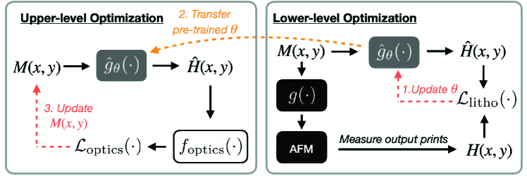
Our solution reformulates the objective in Eq. 1 as a bi-level optimization problem in Fig. 3 [Colson et al., 2007], structured as:
Upper-level (Leader) optimization (subsec. 3.4): Optimize the performance of the computational optics in the specific task based on predictions from the learned lithography simulator (e.g., minimize wavefront error, maximize optical efficiency, or achieve desired functionality). The objective function in Eq. 1 is rewritten as:
| (2) |
where we substitute the unknown underlying lithography system in Eq. 1 with , a digital twin of with parameters learned in the lower-level optimization.
Lower-level (Follower) optimization (subsec. 3.3): Pre-train a lithography digital twin that accurately predicts height profile of the printed structure given input layout . The optimization process is minimizing the difference between the lithography simulator prediction , and the experimentally measured continuous height :
| (3) |
where denotes the loss function for this supervised learning, and here we use the mean absolute error.
To summarize: The leader problem optimizes computational optical element design using the prediction from the neural lithography simulator, learned independently in the follower problem. These interconnected problems, addressed in a bilevel optimization framework, close the design-to-manufacturing gap with robust designs and better optical performance.
3.3. ’Real2Sim’ learning a neural lithography simulator
3.3.1. Lithography forward model.
We construct a physics-based neural network as the differentiable digital twin of the lithography system , referred to as the physics-based learning (PBL) model in this paper. The modeling of the photolithography process normally consists of an optical model and a resist model [Cobb et al., 1996; Chevalier et al., 2021; Lang et al., 2022]:
-
•
The optical model calculates the light exposure dosage distribution on the photoresist, leading to the aerial image;
-
•
The resist model models the photo-chemical reaction and development processes, leading to the final resist profile.
We first illustrate in the context of the general photolithography model and then detail the specific arrangements of the TPL system used in this work. In our context, the resist profile is the ultimate fabricated structure, as it does not undergo further processing steps. Inspired by the work from [Tseng et al., 2022] on photo-finishing, we also apply the pointwise and areawise neural networks inside to model the corresponding operations, respectively (see details in Supplements). Anatomy of the model is visualized in Fig. 4 and details of the sub-models are:
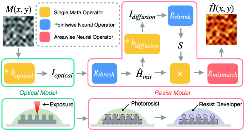
The optical model transforms the input layout mask into an exposure dosage distribution, also known as aerial image, . Depending on the illumination sources, normally incorporate illumination kernel(s), such as a Gaussian point spread function (PSF) under point-source illumination [Auzinger et al., 2018; Saha et al., 2017] or a series of convolution kernels decomposed from transmission-cross coefficient (TCC) matrix in Hopkin’s formulation under Köhler’s illumination [Cobb et al., 1996; Liao et al., 2022]. Specifically, in the point-scanning TPL system used in this work [Harinarayana and Shin, 2021], is modeled as convolution between the mask and a Gaussian PSF with a hyper-parameter being its half-width at half maximum.
The resist model computes the photochemical reaction during exposure and accounts for the structure deformation during development. The initialization of photochemical reaction process is modeled with a pointwise neural network to accurately handle the pixel-wise thresholding operation, resulting in the initial resist profile . Since the diffusion of reactants introduces cross-talk between nearby printed features, we use a Gaussian kernel with a learnable standard deviation to approximate the spatial extent of diffusion [Lang et al., 2022]. As a result, at the end of the reaction we have:
| (4) |
The development process introduces extra deformation to the printed structure, which has been observed to be unidirectional shrinkage perpendicular to the substrate due to the dissolution of soluble components and the capillary forces during the drying process[Meisel et al., 2006; D’Silva et al., 2021]. We model this anisotropic shrinkage with an operation represented by another pointwise neural network, giving . Thus, the resist profile is the product of and after development.
To further mitigate mismatch from the above approximations, we introduce an areawise neural network as a learnable operator , giving the final fabricated structure as:
| (5) |
Chaining the sub-models, we get the predicted height profile of the fabricated structure as:
| (6a) | ||||
| (6b) | ||||
| (6c) | ||||
When applying the ’real2sim’ pipeline to diverse photolithography processes, one cannot rely on a ’one-size-fits-all’ model. To effectively accommodate system-specific or process-dependent variations, hyper-parameters or operations must be fine-tuned. Key among these are or (pertaining to the illumination system) and (associated with the photoresist and its processing protocol). More details about the model architecture and the training process are in the Supplements.
3.3.2. Constructing dataset for learning a lithography simulator
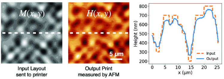
To learn parameterized that enables the optimization of structure, we collect the first dataset in photolithography, where is the size of the dataset, is a random input layout and is the height profile of the fabricated structure, fabricated by a TPL system (Photonic Professional GT2, Nanoscribe GmbH), and measured offline by AFM. Here is the lateral size of the structure. Since the slicing distance along the height direction is 0.1 , and we have levels in our fabrication, the input layouts represent discrete height values from to , providing a phase modulation range from to given a refractive index difference between the fabricated structure and air and illumination wavelength . We register every AFM image with its corresponding input layout with the aid of homography estimation. Fig. 5 shows an example data pair. Details on the fabrication and characterization of the prints are in the Supplements.
3.4. End-to-end co-optimizing design and manufacturability in computational optics
We validate the performance of neural lithography with two representative tasks in computational optics. Below, we present the light transport and design pipeline for each task in Fig. 6. Due to the low absorption property of the fabricated optical element [Li et al., 2019], we treat it as a thin phase object with phase profile . Our work focuses on accurate and omits the variation in as it was reported to be below , the phase variation induced by which is much smaller than that caused by variation of [Dottermusch et al., 2019]. In the design, we use the output from our lithography digital twin for and optimize via auto-differentiation through wave-optics-based forward light transport. We utilize the Gumbel-Softmax reparameterization trick [Jang et al., 2016] to differentiate through the discrete design layout (see details in Supplements).

3.4.1. Holographic optical element
A holographic optical element (HOE) is a micro-structured optical component that generates a desired image or diffraction orders and is commonly used in beam splitting, 3D imaging/display, and augmented reality. We design a HOE for an inline holography system, where the fabricated HOE is expected to generate a pre-designed holographic image at imaging distance upon plane wave illumination. We substitute in Eq. 1 with that calculates the intensity of the electric field after free-space wave propagation of distance with Rayleigh–Sommerfeld convolution [Goodman, 2005]:
| (7a) | ||||
| (7b) |
where is the propagation kernel with . Given a target holographic image , the loss function is:
| (8) |
where is the root mean square error loss, is the energy efficiency, calculated as the sum of intensity inside the region of at image plane divided by the sum of total illumination light intensity.
3.4.2. Multi-level diffractive lens
Compared to conventional refractive lenses, diffractive lenses can perform imaging tasks while being lightweight and compact [Banerji et al., 2019]. We design MDLs with focal length and object to lens distance is . The system’s point spread function (PSF) is the intensity field illuminated by a point source at the object plane. In the context of incoherent imaging under paraxial approximation, the image formation is a shift-invariant convolution of the object with , and the camera records:
| (9a) | ||||
| (9b) | ||||
where is additive Gaussian readout noise. The propagation from the object to the lens is ignored in the calculation because is much larger than the diameter of the lens ( in our case) and we can assume the wavefront from the point source to be flat. Here, we design two types of MDL. The first one is for direct imaging without post-processing the acquired camera recording , and design metric is the focusing efficiency [Banerji et al., 2019] of ; the second one is for in-direct imaging (namely, computational imaging), where we assess the imaging quality after deconvolving by .
Direct imaging: We calculate the PSF’s center-to-background signal ratio (CBR) and the corresponding loss function . Considering that we have a numerical aperture , corresponding to a diffraction-limited focal spot size of , we choose center region size to be and we empirically find this setting leads to the sharpest PSF after the optimization.
yIn-direct/computational imaging: We evaluate the image quality after post-processing [Sitzmann et al., 2018; Tseng et al., 2021]. we apply a fixed Richard-Lucy deconvolution process and calculate the mean absolute error (MAE) between the ground truth and deconvolved result as the loss :
| (10) |
where denotes the deconvolution process, and in this work, we use the Richard-Lucy deconvolution algorithm [Zhao et al., 2018] with iterations.
4. Results
We first evaluate the accuracy and generalizability of our neural lithography simulator in subsection 4.1 (lower-level optimization). Then we present the results of designed and fabricated optical elements in computational optics tasks, in subsections 4.2 and 4.3 (upper-level optimization), which show the priority of our pipeline in mitigating the design-to-manufacturing gap. We further provide detailed results to visualize the improvement by our pipeline in subsection 4.4 and noise analysis to investigate the performance limit of our method in subsection 4.5.
4.1. Forward predicting capability
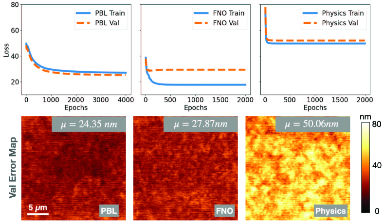
We evaluate the efficacy for , trained from the dataset described in section 3.3.2 and Fig 5. We visualize the loss curves and error maps that compare our PBL model with other learnable modeling approaches, including the parameterized physics model [Lang et al., 2022] and Fourier Neural Operator (FNO) [Yang et al., 2022b]. The details of the models and training hyperparameters are in the Supplements. We show that the PBL modeling receives the lowest validation loss and error. The parameterized physics model has limited degrees of freedom and thus cannot fully fit the data. Without applying the physics model as a prior, FNO exhibits good fitting ability while tending to overfit on the training set.
4.2. Application: Holographic optical element
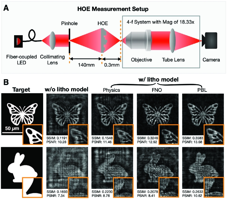
We design several HOEs with the three lithography models using the pipeline in subsection 3.4.1. The traditional design without a lithography model in the loop is also added as a reference. The designed input layouts are with an optimizable pitch size of and optimized with Adam for 1000 iterations under a learning rate of . We capture holographic images of the fabricated HOEs with the setup sketched in Fig. 8A. As expected, the resulting images with lithography models present better image quality and contrast. We also assess the SSIM and PSNR of the images using the Kornia package [Riba et al., 2020], where the one optimized using the PBL model scores the highest. The overall low value of the SSIM and PSNR may come from the measurement system’s misalignment and the layout’s limited quantization levels.
4.3. Application: Multi-level diffractive lens
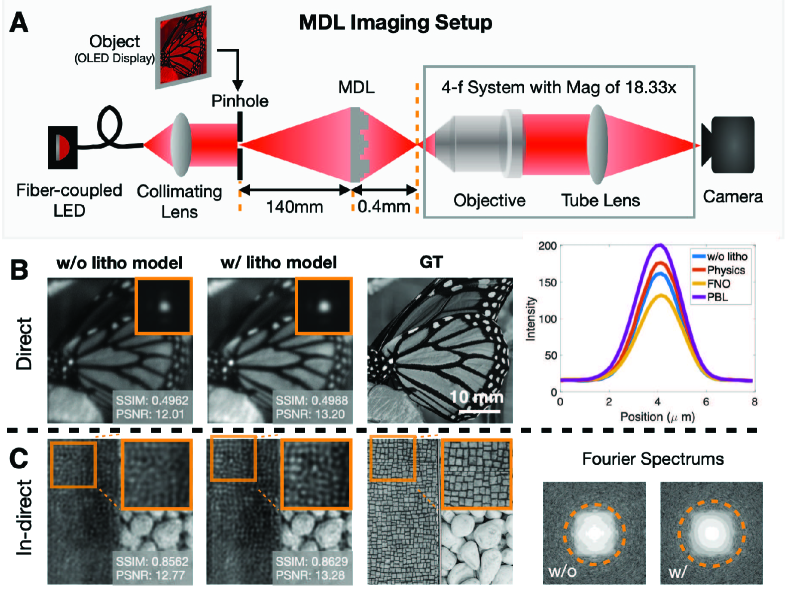
We compare the performance of our designed and fabricated MDLs to investigate the performance gain brought by the neural lithography (Fig. 9). The designed MDL layouts are with an optimizable pitch size of and optimized with AdamW for 1000 iterations under a learning rate of . We built a system sketched in Fig. 9A, where the pinhole is used to calibrate the PSF of the imaging system. During imaging, we switch the light path to the object plane (the OLED display), which is in conjugation with the pinhole plane.
The direct imaging outcomes (Fig. 9B) demonstrate the imaging contrast bolstered by the PBL lithography simulator’s inclusion in the design loop. Further profiling of PSFs associated with various MDLs reveals that the design aided with the PBL model yields the brightest PSF. Furthermore, the computational imaging result in Fig. 9C shows that when both deconvolving with the camera-captured (calibrated) PSFs, the one with the neural lithography simulator results in more details, which retains the higher-frequency imaging capability, as highlighted in the zoom-in view. Post-calibration has been used to mitigate fabrication inaccuracy in previous work [Tseng et al., 2021], but the comparison here shows that it cannot fully address the issue. This is also evidenced by the Fourier spectrum of the PSFs shown on the right-hand side of Fig. 9C, where the Fourier spectrum corresponding to the PSF associated with the PBL litho model exhibits higher frequency coverage.

4.4. Design-to-manufacturing gap mitigation
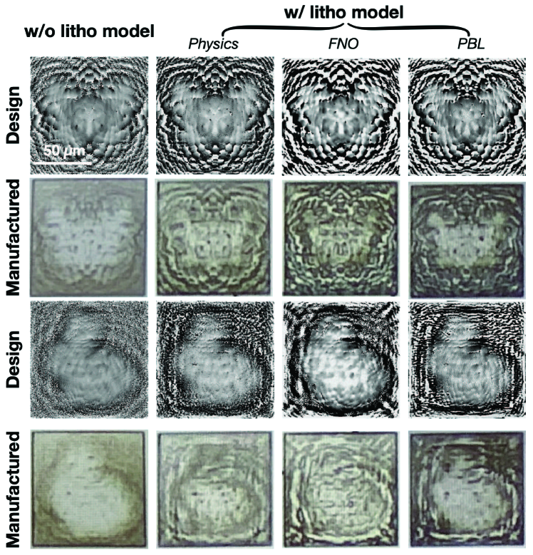
In Fig. 10, we show the layout of the designed HOEs and optical micrographs of the corresponding fabricated structure. We observe more high-frequency features in the designs without the lithography model and a smoother profile in the designs with the lithography model. Also, there is a better coincidence between designs and prints when using our PBL lithography model in the design loop. In contrast, a large mismatch exists between design and print without a neural photolithography simulator. This evidences the lithography model serves as a regularizer on fabrication feasibility during the design process.
A quantitative comparison of the holographic images of the HOEs (micrographs of which are in Fig. 10) in both design and experiment in Fig. 11 reinforces our conclusion. The ones without the lithography model show the highest SSIM in the design while being the worst in the experimental measurement. Given the huge design-to-manufacturing gap in Fig. 11, it is unsurprising. The images using our neural photolithography simulator show the highest SSIM in manufacturing while maintaining the lowest gap between the design and manufacturing values. The comparison between the Physics and PBL models in the figure reveals that the PBL model does more than just add parameterized smoothness to the design profile, as the Physics model does. Instead, it captures more complex physical relationships, thereby better mitigating the design-to-manufacturing gap.
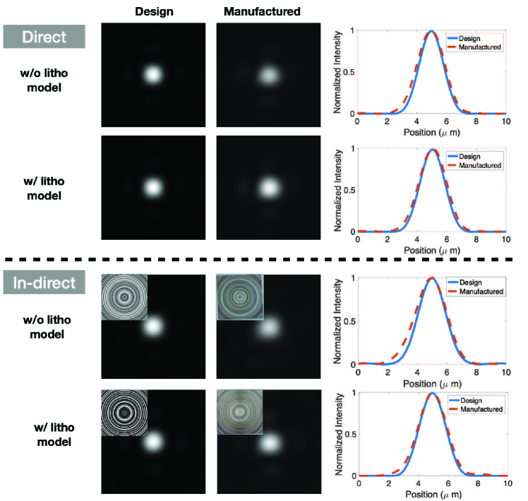
Similarly, the effectiveness of our method in creating multi-level diffractive lenses is evidenced by the PSFs displayed in Fig. 12. In both direct and computational imaging scenarios, the line profiles across the center of the PSFs from MDLs designed using the lithography model show a better fit to the design than those lacking the lithography model. Additionally, in the direct imaging case, the PSF with the lithography model displays higher overall brightness. In the computational imaging case, there is greater correspondence between the design and the resulting optical micrograph when using the lithography model.
4.5. Analyze noise to the aleatoric uncertainty
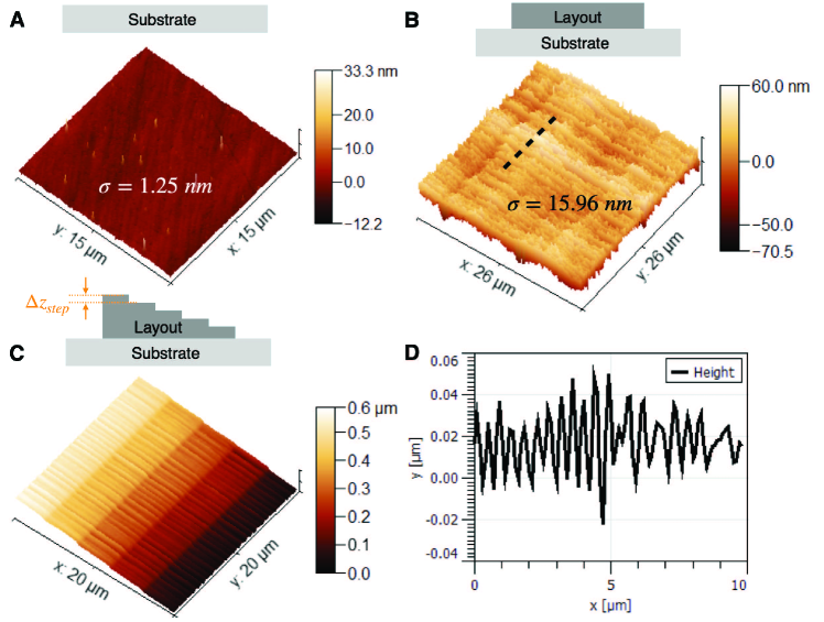
The ultimate predicting ability of our lithography simulator depends on both the model’s learning ability and the dataset’s quality, relating to the model’s epistemic uncertainty and the dataset’s aleatoric uncertainty, respectively [Hüllermeier and Waegeman, 2021]. In Fig. 13, we visualize and quantify noises by fabricating a flat surface (Fig. 13B) and a 5-step structure (Fig. 13C) and measuring them together with a flat substrate (Fig. 13A). Comparison between Fig. 13A and Fig. 13B shows that the unmodeled fabrication error is the dominant noise source in our TPL demonstration. While the roughness of a clean substrate without printed features is (Fig. 13A), the printed flat surface shows roughness of , resulting from the non-periodic line-shaped features post-fabrication. We further plot a height profile of these features along the black dashed line on the flat surface in Fig. 13D, where the randomness in the plot evidences these line-shaped features are hard to model. We also observe these features in the fabricated 5-step structure, but the step size can still be well identified, indicating the structure is well recognized in large structures. Given these, our predicting error of using PBL indicates future room to improve our , such as with more training data or more intricate model considering these line-shaped features, or even switching to projective photolithography systems. Nevertheless, reveals an upper performance bound of current given the TPL system we use.
5. Discussion
Limitations:
-
•
The data noise during fabrication and measurement fundamentally limits the optimization capability.
-
•
The neural photolithography simulator has no theoretical guarantees, which might produce adverse designs in the ill-posed inverse design procedures.
-
•
The sim2real gap between simulated and real optical systems impairs performance. The post-calibration methods mitigate the sim2real gap but don’t correct the bias from incorrect modeling during design.
Future work: As a first work on differentiable/neural lithography, our work is poised to inspire future investigations:
Applying to other design and fabrication processes. Our real2sim pipeline is adaptable to various lithography techniques, each requiring fine-tuning the model architecture. For example, extreme ultraviolet (EUV) lithography necessitates extra modeling for reflective projection optics [Wagner and Harned, 2010], while etching-based or nanoimprint methods require an added step to transform the resist profile into the final structure [Barcelo and Li, 2016]. Similarly, e-beam lithography involves a more complex PSF from electron scattering [Koleva et al., 2018]. Moreover, future work can investigate applying our end-to-end co-optimization pipeline to design and fabricate more complex downstream tasks, such as obtaining depth profile from defocus [Ikoma et al., 2021] and implementing optical computing [Goi et al., 2022].
Further improving the pipeline. On the hardware side, other characterization tools, such as 3D SEM [Tafti et al., 2015] or EUV diffractive imaging [Gardner et al., 2017], could be further explored for collecting high-throughput and high-accuracy datasets. On the algorithm side, comprehensive 3D modeling instead of 2.5D will cover more complex resist profiles. We can also further incorporate advanced modeling like neural architecture searching [Ba et al., 2019] to improve the precision of photolithography predictions or utilize implicit neural fields [Yang et al., 2021] to augment the design efficiency of neural lithography.
Conclusion: To conclude, our study unveils a unique perspective of jointly optimizing diffractive optical elements in computational optics and their fabrication feasibility. By employing a ’real2sim’ learned digital twin of the photolithography system, we enhance the outcomes of optical tasks. This methodology paves the way for the precise manufacturing of sophisticated computational optics elements, expediting their introduction to commercial products. We anticipate that the ’real2sim’ approach presented in this paper will encourage both industry and academia to complement traditional white-box methods with the more adaptive, data-driven gray-box methodologies for modeling computational optics systems, as exemplified by the lithography system discussed in our work.
Acknowledgements.
This work is supported by NIH (5-P41-EB015871), Fujikura Limited, and the Hong Kong Innovation and Technology Fund (ITS/178/20FP). This work was carried out in part using MIT.nano’s facilities.References
- [1]
- Arthur and Martin [1996] Graham Arthur and Brian Martin. 1996. Investigation of photoresist-specific optical proximity effect. Microelectronic engineering 30, 1-4 (1996), 133–136.
- Auzinger et al. [2018] Thomas Auzinger, Wolfgang Heidrich, and Bernd Bickel. 2018. Computational design of nanostructural color for additive manufacturing. ACM Transactions on Graphics (TOG) 37, 4 (2018), 1–16.
- Ba et al. [2019] Yunhao Ba, Guangyuan Zhao, and Achuta Kadambi. 2019. Blending diverse physical priors with neural networks. arXiv preprint arXiv:1910.00201 (2019).
- Baek et al. [2021] Seung-Hwan Baek, Hayato Ikoma, Daniel S Jeon, Yuqi Li, Wolfgang Heidrich, Gordon Wetzstein, and Min H Kim. 2021. Single-shot hyperspectral-depth imaging with learned diffractive optics. In Proceedings of the IEEE/CVF International Conference on Computer Vision. 2651–2660.
- Banerji et al. [2019] Sourangsu Banerji, Monjurul Meem, Apratim Majumder, Fernando Guevara Vasquez, Berardi Sensale-Rodriguez, and Rajesh Menon. 2019. Imaging with flat optics: metalenses or diffractive lenses? Optica 6, 6 (2019), 805–810.
- Barcelo and Li [2016] Steven Barcelo and Zhiyong Li. 2016. Nanoimprint lithography for nanodevice fabrication. Nano Convergence 3, 1 (2016), 1–9.
- Baydin et al. [2018] Atilim Gunes Baydin, Barak A Pearlmutter, Alexey Andreyevich Radul, and Jeffrey Mark Siskind. 2018. Automatic differentiation in machine learning: a survey. Journal of Marchine Learning Research 18 (2018), 1–43.
- Blachowicz et al. [2021] Tomasz Blachowicz, Guido Ehrmann, and Andrea Ehrmann. 2021. Optical elements from 3D printed polymers. e-Polymers 21, 1 (2021), 549–565.
- Boominathan et al. [2020] Vivek Boominathan, Jesse K Adams, Jacob T Robinson, and Ashok Veeraraghavan. 2020. Phlatcam: Designed phase-mask based thin lensless camera. IEEE transactions on pattern analysis and machine intelligence 42, 7 (2020), 1618–1629.
- Cecil et al. [2022] Thomas Cecil, Danping Peng, Daniel Abrams, Stanley J Osher, and Eli Yablonovitch. 2022. Advances in Inverse Lithography. ACS Photonics (2022).
- Chakravarthula et al. [2020] Praneeth Chakravarthula, Ethan Tseng, Tarun Srivastava, Henry Fuchs, and Felix Heide. 2020. Learned hardware-in-the-loop phase retrieval for holographic near-eye displays. ACM Transactions on Graphics (TOG) 39, 6 (2020), 1–18.
- Chevalier et al. [2021] Pierre Chevalier, Patrick Quéméré, Sébastien Bérard-Bergery, Jean-Baptiste Henry, Charlotte Beylier, and Jérôme Vaillant. 2021. Rigorous Model-Based Mask Data Preparation Algorithm Applied to Grayscale Lithography for the Patterning at the Micrometer Scale. Journal of Microelectromechanical Systems 30, 3 (2021), 442–455.
- Choi et al. [2022] Suyeon Choi, Manu Gopakumar, Yifan Peng, Jonghyun Kim, Matthew O’Toole, and Gordon Wetzstein. 2022. Time-multiplexed neural holography: a flexible framework for holographic near-eye displays with fast heavily-quantized spatial light modulators. In ACM SIGGRAPH 2022 Conference Proceedings. 1–9.
- Cobb et al. [1996] Nicolas B Cobb, Avideh Zakhor, and Eugene A Miloslavsky. 1996. Mathematical and CAD framework for proximity correction. In Optical Microlithography IX, Vol. 2726. SPIE, 208–222.
- Colson et al. [2007] Benoît Colson, Patrice Marcotte, and Gilles Savard. 2007. An overview of bilevel optimization. Annals of operations research 153 (2007), 235–256.
- Dong et al. [2003] Chen-Yuan Dong, Karsten Koenig, and Peter So. 2003. Characterizing point spread functions of two-photon fluorescence microscopy in turbid medium. Journal of biomedical optics 8, 3 (2003), 450–459.
- Dottermusch et al. [2019] Stephan Dottermusch, Dmitry Busko, Malte Langenhorst, Ulrich W Paetzold, and Bryce S Richards. 2019. Exposure-dependent refractive index of Nanoscribe IP-Dip photoresist layers. Optics letters 44, 1 (2019), 29–32.
- D’Silva et al. [2021] Sean D’Silva, Thomas Mülders, Hans-Jürgen Stock, and Andreas Erdmann. 2021. Modeling the impact of shrinkage effects on photoresist development. Journal of Micro/Nanopatterning, Materials, and Metrology 20, 1 (2021), 014602–014602.
- Gardner et al. [2017] Dennis F Gardner, Michael Tanksalvala, Elisabeth R Shanblatt, Xiaoshi Zhang, Benjamin R Galloway, Christina L Porter, Robert Karl Jr, Charles Bevis, Daniel E Adams, Henry C Kapteyn, et al. 2017. Subwavelength coherent imaging of periodic samples using a 13.5 nm tabletop high-harmonic light source. Nature Photonics 11, 4 (2017), 259–263.
- Giessibl [2003] Franz J Giessibl. 2003. Advances in atomic force microscopy. Reviews of modern physics 75, 3 (2003), 949.
- Goi et al. [2022] Elena Goi, Steffen Schoenhardt, and Min Gu. 2022. Direct retrieval of Zernike-based pupil functions using integrated diffractive deep neural networks. Nature Communications 13, 1 (2022), 7531.
- Goodman [2005] Joseph W Goodman. 2005. Introduction to Fourier optics. Roberts and Company publishers.
- Gostimirovic et al. [2022] Dusan Gostimirovic, Dan-Xia Xu, Odile Liboiron-Ladouceur, and Yuri Grinberg. 2022. Deep Learning-Based Prediction of Fabrication-Process-Induced Structural Variations in Nanophotonic Devices. ACS Photonics 9, 8 (2022), 2623–2633.
- Hahn et al. [2020] Vincent Hahn, Pascal Kiefer, Tobias Frenzel, Jingyuan Qu, Eva Blasco, Christopher Barner-Kowollik, and Martin Wegener. 2020. Rapid assembly of small materials building blocks (voxels) into large functional 3D metamaterials. Advanced Functional Materials 30, 26 (2020), 1907795.
- Harinarayana and Shin [2021] V Harinarayana and YC Shin. 2021. Two-photon lithography for three-dimensional fabrication in micro/nanoscale regime: A comprehensive review. Optics & Laser Technology 142 (2021), 107180.
- Hong et al. [2021] Zhihan Hong, Piaoran Ye, Douglas A Loy, and Rongguang Liang. 2021. Three-dimensional printing of glass micro-optics. Optica 8, 6 (2021), 904–910.
- Hüllermeier and Waegeman [2021] Eyke Hüllermeier and Willem Waegeman. 2021. Aleatoric and epistemic uncertainty in machine learning: An introduction to concepts and methods. Machine Learning 110 (2021), 457–506.
- ICRA [2023] ICRA. 2023. Real2Sim in ICRA 2023. {https://real2sim.com/} Accessed: May 14, 2023.
- Ikoma et al. [2021] Hayato Ikoma, Cindy M Nguyen, Christopher A Metzler, Yifan Peng, and Gordon Wetzstein. 2021. Depth from defocus with learned optics for imaging and occlusion-aware depth estimation. In 2021 IEEE International Conference on Computational Photography (ICCP). IEEE, 1–12.
- Intel [2023] Intel. 2023. Intel® RealSense™ Depth Camera. {https://www.intelrealsense.com/depth-camera-d415/} Accessed: May 14, 2023.
- Jang et al. [2022] Changwon Jang, Kiseung Bang, Minseok Chae, Byoungho Lee, and Douglas Lanman. 2022. Waveguide Holography: Towards True 3D Holographic Glasses. arXiv preprint arXiv:2211.02784 (2022).
- Jang et al. [2020] Changwon Jang, Olivier Mercier, Kiseung Bang, Gang Li, Yang Zhao, and Douglas Lanman. 2020. Design and fabrication of freeform holographic optical elements. ACM Transactions on Graphics (TOG) 39, 6 (2020), 1–15.
- Jang et al. [2016] Eric Jang, Shixiang Gu, and Ben Poole. 2016. Categorical reparameterization with gumbel-softmax. arXiv preprint arXiv:1611.01144 (2016).
- Jiang et al. [2020] Bentian Jiang, Lixin Liu, Yuzhe Ma, Hang Zhang, Bei Yu, and Evangeline FY Young. 2020. Neural-ILT: Migrating ILT to neural networks for mask printability and complexity co-optimization. In Proceedings of the 39th International Conference on Computer-Aided Design. 1–9.
- Kingma and Ba [2014] Diederik P Kingma and Jimmy Ba. 2014. Adam: A method for stochastic optimization. arXiv preprint arXiv:1412.6980 (2014).
- Koleva et al. [2018] E Koleva, K Vutova, B Asparuhova, I Kostic, K Cvetkov, and V Gerasimov. 2018. Modeling approaches for electron beam lithography. In Journal of Physics: Conference Series, Vol. 1089. IOP Publishing, 012016.
- Kuo et al. [2020] Grace Kuo, Laura Waller, Ren Ng, and Andrew Maimone. 2020. High resolution étendue expansion for holographic displays. ACM Transactions on Graphics (TOG) 39, 4 (2020), 66–1.
- Lang et al. [2022] Nicolas Lang, Sven Enns, Julian Hering, and Georg von Freymann. 2022. Towards efficient structure prediction and pre-compensation in multi-photon lithography. Optics Express 30, 16 (2022), 28805–28816.
- Lee et al. [2023] Kyung Chul Lee, Junghyun Bae, Nakkyu Baek, Jaewoo Jung, Wook Park, and Seung Ah Lee. 2023. Design and single-shot fabrication of lensless cameras with arbitrary point spread functions. Optica 10, 1 (2023), 72–80.
- Levin et al. [2013] Anat Levin, Daniel Glasner, Ying Xiong, Frédo Durand, William Freeman, Wojciech Matusik, and Todd Zickler. 2013. Fabricating BRDFs at high spatial resolution using wave optics. ACM Transactions on Graphics (TOG) 32, 4 (2013), 1–14.
- Li et al. [2019] Y Li, S Park, M McLamb, M Lata, S Schöche, D Childers, ID Aggarwal, MK Poutous, G Boreman, and Tino Hofmann. 2019. UV to NIR optical properties of IP-Dip, IP-L, and IP-S after two-photon polymerization determined by spectroscopic ellipsometry. Optical Materials Express 9, 11 (2019), 4318–4328.
- Li et al. [2020] Zongyi Li, Nikola Kovachki, Kamyar Azizzadenesheli, Burigede Liu, Kaushik Bhattacharya, Andrew Stuart, and Anima Anandkumar. 2020. Fourier neural operator for parametric partial differential equations. arXiv preprint arXiv:2010.08895 (2020).
- Liao et al. [2022] Wei-Ping Liao, Hsueh-Li Liu, Yu-Fan Lin, Sheng-Siang Su, Yu-Teng Chen, Guan-Bo Lin, Tsung-Chieh Tseng, Tong-Ke Lin, Chun-Chi Chen, Wen-Hsien Huang, et al. 2022. I-line photolithographic metalenses enabled by distributed optical proximity correction with a deep-learning model. Optics Express 30, 12 (2022), 21184–21194.
- Meisel et al. [2006] Daniel Christoph Meisel, Marcus Diem, Markus Deubel, Fabián Pérez-Willard, Stefan Linden, Dagmar Gerthsen, Kurt Busch, and Martin Wegener. 2006. Shrinkage precompensation of holographic three-dimensional photonic-crystal templates. advanced materials 18, 22 (2006), 2964–2968.
- Metzler et al. [2020] Christopher A Metzler, Hayato Ikoma, Yifan Peng, and Gordon Wetzstein. 2020. Deep optics for single-shot high-dynamic-range imaging. In Proceedings of the IEEE/CVF Conference on Computer Vision and Pattern Recognition. 1375–1385.
- Orange-Kedem et al. [2021] Reut Orange-Kedem, Elias Nehme, Lucien E Weiss, Boris Ferdman, Onit Alalouf, Nadav Opatovski, and Yoav Shechtman. 2021. 3D printable diffractive optical elements by liquid immersion. Nature communications 12, 1 (2021), 3067.
- Peng et al. [2020] Yifan Peng, Suyeon Choi, Nitish Padmanaban, and Gordon Wetzstein. 2020. Neural holography with camera-in-the-loop training. ACM Transactions on Graphics (TOG) 39, 6 (2020), 1–14.
- Poonawala and Milanfar [2007] Amyn Poonawala and Peyman Milanfar. 2007. Mask design for optical microlithography—an inverse imaging problem. IEEE Transactions on Image Processing 16, 3 (2007), 774–788.
- Riba et al. [2020] Edgar Riba, Dmytro Mishkin, Daniel Ponsa, Ethan Rublee, and Gary Bradski. 2020. Kornia: an open source differentiable computer vision library for pytorch. In Proceedings of the IEEE/CVF Winter Conference on Applications of Computer Vision. 3674–3683.
- Roques-Carmes et al. [2022] Charles Roques-Carmes, Zin Lin, Rasmus E Christiansen, Yannick Salamin, Steven E Kooi, John D Joannopoulos, Steven G Johnson, and Marin Soljacic. 2022. Toward 3D-printed inverse-designed metaoptics. ACS Photonics 9, 1 (2022), 43–51.
- Saha et al. [2017] Sourabh K Saha, Chuck Divin, Jefferson A Cuadra, and Robert M Panas. 2017. Effect of proximity of features on the damage threshold during submicron additive manufacturing via two-photon polymerization. Journal of Micro and Nano-Manufacturing 5, 3 (2017).
- Sitzmann et al. [2018] Vincent Sitzmann, Steven Diamond, Yifan Peng, Xiong Dun, Stephen Boyd, Wolfgang Heidrich, Felix Heide, and Gordon Wetzstein. 2018. End-to-end optimization of optics and image processing for achromatic extended depth of field and super-resolution imaging. ACM Transactions on Graphics (TOG) 37, 4 (2018), 1–13.
- Sun et al. [2020a] Qilin Sun, Ethan Tseng, Qiang Fu, Wolfgang Heidrich, and Felix Heide. 2020a. Learning rank-1 diffractive optics for single-shot high dynamic range imaging. In Proceedings of the IEEE/CVF conference on computer vision and pattern recognition. 1386–1396.
- Sun et al. [2020b] Qilin Sun, Jian Zhang, Xiong Dun, Bernard Ghanem, Yifan Peng, and Wolfgang Heidrich. 2020b. End-to-end learned, optically coded super-resolution SPAD camera. ACM Transactions on Graphics (TOG) 39, 2 (2020), 1–14.
- Synopsys [2023] Synopsys. 2023. S-Litho: Predictive Modeling of Lithographic Processes. {https://www.synopsys.com/silicon/mask-synthesis/sentaurus-lithography.html} Accessed: Aug 27, 2023.
- Tafti et al. [2015] Ahmad P Tafti, Andrew B Kirkpatrick, Zahrasadat Alavi, Heather A Owen, and Zeyun Yu. 2015. Recent advances in 3D SEM surface reconstruction. Micron 78 (2015), 54–66.
- Tan et al. [2021] Shiyu Tan, Yicheng Wu, Shoou-I Yu, and Ashok Veeraraghavan. 2021. Codedstereo: Learned phase masks for large depth-of-field stereo. In Proceedings of the IEEE/CVF Conference on Computer Vision and Pattern Recognition. 7170–7179.
- Tseng et al. [2021] Ethan Tseng, Shane Colburn, James Whitehead, Luocheng Huang, Seung-Hwan Baek, Arka Majumdar, and Felix Heide. 2021. Neural nano-optics for high-quality thin lens imaging. Nature communications 12, 1 (2021), 6493.
- Tseng et al. [2019] Ethan Tseng, Felix Yu, Yuting Yang, Fahim Mannan, Karl ST Arnaud, Derek Nowrouzezahrai, Jean-François Lalonde, and Felix Heide. 2019. Hyperparameter optimization in black-box image processing using differentiable proxies. ACM Trans. Graph. 38, 4 (2019), 27–1.
- Tseng et al. [2022] Ethan Tseng, Yuxuan Zhang, Lars Jebe, Xuaner Zhang, Zhihao Xia, Yifei Fan, Felix Heide, and Jiawen Chen. 2022. Neural Photo-Finishing. ACM Transactions on Graphics (TOG) 41, 6 (2022), 1–15.
- Wagner and Harned [2010] Christian Wagner and Noreen Harned. 2010. Lithography gets extreme. Nature Photonics 4, 1 (2010), 24–26.
- Wang et al. [2020] Hao Wang, Hongtao Wang, Wang Zhang, and Joel KW Yang. 2020. Toward near-perfect diffractive optical elements via nanoscale 3D printing. ACS nano 14, 8 (2020), 10452–10461.
- Yang et al. [2021] Guandao Yang, Serge Belongie, Bharath Hariharan, and Vladlen Koltun. 2021. Geometry processing with neural fields. Advances in Neural Information Processing Systems 34 (2021), 22483–22497.
- Yang et al. [2018] Haoyu Yang, Shuhe Li, Yuzhe Ma, Bei Yu, and Evangeline FY Young. 2018. GAN-OPC: Mask optimization with lithography-guided generative adversarial nets. In Proceedings of the 55th Annual Design Automation Conference. 1–6.
- Yang et al. [2022a] Haoyu Yang, Zongyi Li, Kumara Sastry, Saumyadip Mukhopadhyay, Anima Anandkumar, Brucek Khailany, Vivek Singh, and Haoxing Ren. 2022a. Large Scale Mask Optimization Via Convolutional Fourier Neural Operator and Litho-Guided Self Training. arXiv preprint arXiv:2207.04056 (2022).
- Yang et al. [2022b] Haoyu Yang, Zongyi Li, Kumara Sastry, Saumyadip Mukhopadhyay, Mark Kilgard, Anima Anandkumar, Brucek Khailany, Vivek Singh, and Haoxing Ren. 2022b. Generic lithography modeling with dual-band optics-inspired neural networks. In Proceedings of the 59th ACM/IEEE Design Automation Conference. 973–978.
- Ye et al. [2019] Wei Ye, Mohamed Baker Alawieh, Yibo Lin, and David Z Pan. 2019. LithoGAN: End-to-end lithography modeling with generative adversarial networks. In Proceedings of the 56th Annual Design Automation Conference 2019. 1–6.
- You et al. [2020] Shangting You, Jiaao Guan, Jeffrey Alido, Henry H Hwang, Ronald Yu, Leilani Kwe, Hao Su, and Shaochen Chen. 2020. Mitigating scattering effects in light-based three-dimensional printing using machine learning. Journal of Manufacturing Science and Engineering 142, 8 (2020), 081002.
- Zhao et al. [2018] Guangyuan Zhao, Cheng Zheng, Cuifang Kuang, Renjie Zhou, Mohammad M Kabir, Kimani C Toussaint Jr, Wensheng Wang, Liang Xu, Haifeng Li, Peng Xiu, et al. 2018. Nonlinear focal modulation microscopy. Physical review letters 120, 19 (2018), 193901.
- Zhou et al. [2014] Mingdong Zhou, Boyan S Lazarov, and Ole Sigmund. 2014. Topology optimization for optical projection lithography with manufacturing uncertainties. Applied optics 53, 12 (2014), 2720–2729.
- Zhu et al. [2022] Xiaopei Zhu, Zhanhao Hu, Siyuan Huang, Jianmin Li, and Xiaolin Hu. 2022. Infrared invisible clothing: Hiding from infrared detectors at multiple angles in real world. In Proceedings of the IEEE/CVF Conference on Computer Vision and Pattern Recognition. 13317–13326.
Appendix A Differentiating through multi-level diffractive optical elements with Gumbel-Softmax trick
The leader optimization in the main text requires the pipeline to be fully differentiable. However, the quantization levels of the mask layout are limited in many photolithography fabrication processes, including the two-photon lithography (TPL) system we use in this work. The Nanoscribe TPL system has a minimum axial slicing distance of . That is to say, it only supports discrete height inputs instead of a continuous height profile between 0 and , and we calculate that it has 12 discrete levels, leading to , to be random discrete values from 222Here we abuse the use of notations. Normally contains and here we refer it as .. Thus, we apply the Gumbel-Softmax trick [Jang et al., 2016] on the categorical height variables to allow for sampling from the categorical distribution during the forward pass through our lithography simulator. It is worth mentioning that this trick has recently been used in other computational optics tasks [Choi et al., 2022; Zhu et al., 2022].
For each pixel in the layout , we model it follows categorical distribution with class probabilities , corresponding to the categories, i.e., quantized phase levels.
We introduce Gumbel noise to add randomness to the sampling procedure.
| (11) |
where is the Gumbel noise. We then calculate the vector using softmax as a differentiable approximation to the argmax-based sampling:
| (12) |
where we choose temperature in our experiment. See more explanations of Gumble-Softmax in [Jang et al., 2016].

Appendix B Fabrication and characterization
B.1. Mask and optical elements fabrication
We fabricate the masks in dataset and computational optical elements in downstream tasks using a commercial two-photon lithography system – Photonic Professional GT2 (Nanoscribe GmbH). We use a 63×/1.4NA objective, IP-Dip photoresist, and a fused silica glass substrate.
We follow the printing parameter set according to [Wang et al., 2020], reproducing very well in our task. The writing parameters for the photolithography process are fixed for all prints: the ratio of laser power , scan speed , and hatching and slicing distance of 0.1 .
The laser power ratio is critical for the lithography performance. We grid-search the laser power in case it leads to poor manufacturing. As seen from Fig. 14, a laser power is the most suitable for printing the structure and would neither over- nor under-expose the photoresist.
A 1--thick base layer is printed with the same parameters before printing the structures to compensate for errors in identifying the position of the substrate and resist interface. After photopolymerization, the structures are developed in resist developer polyethylene glycol methyl ether acetate (PGMEA) for 20 min, followed by immersion in isopropyl alcohol for 5 min. Then, we use a nitrogen gun to dry the structures before deployment.
B.2. Prints characterization
We measure the height profiles of the fabricated structures using Jupiter XR atomic force microscope (AFM) (Asylum Research, Oxford Instruments). We choose to use the AFM based on the performance comparison of the three mainstream methods: the Profilometer [Hong et al., 2021], SEM [Liao et al., 2022], and AFM [Chevalier et al., 2021], which all have been used for characterizing the nano-optical prints before. AFM provides quantitative information on structure height with a high lateral resolution, while SEM doesn’t have quantitative height information, and Profilometer doesn’t have enough lateral resolution.
| Profilometer | SEM | AFM | |
|---|---|---|---|
| Lateral Resolution | Low | High | High |
| Speed | Fast | Medium | Slow |
| Dimension | 2.5D | 2D | 2.5D |
We acquire the AFM images with a scanning pixel size. We then process the images in Gwyddion333http://gwyddion.net/ software to remove the background with order polynomial fit and shift the minimum height value to .
Appendix C Generate randomized printing layout
To efficiently explore the design space of layout to train a for the inverse design, we design the height layout () to be random discrete values from . The mathematical operation to synthesize is in Eq. 13, modified from [Gostimirovic et al., 2022]. We sample a matrix with each entry . We then apply a low-pass filter (LPF) on the Fourier transform of this random matrix to remove the high-frequency structural components; an inverse Fourier transform is applied on the normalized real part of it. Finally, we apply a quantization step , which quantizes the layout pixel values to .
| (13a) |
| (13b) |
where is the step size for the quantization, denotes normalizing the input to . The final layouts contain structures of lateral sizes ranging from to several microns.
Appendix D Model architecture and training settings
D.1. Training details
When training the forward model in the main text, we split the dataset to train set size and validation set size . We compare the three models: the PBL, the Fourier Neural Operator (FNO), and the parameterized physics model. These three models are trained using the Adam optimizer [Kingma and Ba, 2014] and a batchsize of for epochs. Specifically, the learning rate for training the PBL model is . Note that the neural lithography simulator should be retrained for every new fabrication system or a new photoresist/protocol.
D.2. Model architecture
D.2.1. More details on the PBL model.
Table 3 summarizes the learnable parameters in lithography simulator . There are single-value parameters in the corresponding Gaussian kernels and learnable weights and biases of the convolution layers inside each neural operator.
We do not include into as it is deterministic concerning the optical setup. is fixed as , calculated according to the beam focused by the illumination objective lens [Dong et al., 2003]. is learnable. To limit ’s range during the training, we further model as:
| (14) |
where is a hyper-parameter to limit the value range, and is the underlying learnable parameter. Specifically, in this work, we determine ’s value range to be [0, ] according to [Lang et al., 2022] and thus set the hyper-parameter .
| Function | Parameter |
|---|---|
| Weights and biases | |
| Weights and biases | |
| Weights and biases |
We apply the pointwise and areawise neural networks inside the physics-based neural network to model the corresponding operations inspired by the work from [Tseng et al., 2022].
Pointwise neural operator is used in and . It affects the input at a pixel-wise level without affecting neighboring pixels. As summarized in Table 4 below, it consists of three convolution layers using a kernel, each followed by a Leaky Relu activation function (with the hyper-parameter negative slope ) except for the last layer.
| Layer Name | Output Channels | Kernel Size | Activation |
|---|---|---|---|
| Conv1 | 128 | LeakyReLU | |
| Conv2 | 64 | LeakyReLU | |
| Conv3 | 1 | - |
Areawise neural operator is used in . It is a nonlinear filter that depends on patches or segments of the input (e.g., regions of an image) rather than individual pixels. Thus, we use convolution layers with kernel size as a and padding size as . Table 5 below shows five convolution layers, each followed by a Leaky Relu activation function () except for the last layer.
| Layer Name | Output Channels | Kernel Size | Activation |
|---|---|---|---|
| Conv1 | 64 | LeakyReLU | |
| Conv2 | 64 | LeakyReLU | |
| Conv3 | 32 | LeakyReLU | |
| Conv4 | 32 | LeakyReLU | |
| Conv5 | 1 | - |
D.2.2. Fourier Neural Operator (FNO)
Our implementation of the FNO model is adapted from FNO2d in [Li et al., 2020]. Key hyperparameters are: ; ; . We use a learning rate of for training the FNO model.
D.2.3. Parameterized physics model (Physics)
The parameterized physics model is modified from our PBL model but substitutes the neural network modules with parameterized functions. Modifications include:
-
•
Substituting the pointwise neural network with a normalized projection [Zhou et al., 2014]:
(15) where and are learnable single-value parameters. The function does not differ too much from sigmoid (normally used to represent the threshold behavior of photoresist) when is large. We use it because, for a small , this function is better as it interpolates the whole interval [0,1], but the sigmoid function does not.
-
•
Substituting the pointwise neural network with a linear mapping operation used in [Lang et al., 2022]:
(16) where is the learnable single-value parameter and is fixed to be 1.
-
•
Substituting the areawise neural network with a learnable single-value height bias .
To summarize, in the parameterized physics model, they are learnable single-value parameters: , , , and , which is used to parameterize the kernel for the diffusion of reactants. The learning rate for training the parameterized physics model is .
Appendix E Additional Experimental Details
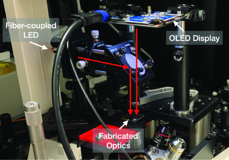
The experimental setup in Fig. 15, incorporates two illumination sources. For holographic imaging and the acquisition of the PSF, we utilize a fiber-coupled LED collimated to pass through a pinhole and then reflected by a mirror onto the fabricated optics. In MDL imaging, the fiber-coupled LED beam path is removed, and an OLED display serves as the object with dimensions of . The exposure times for capturing holographic and MDL images are and , respectively. These extended durations are attributable to low illumination power and camera quantum efficiency. We also note the presence of dead pixels on the camera (CMOS, FLIR GS3-U3-32S4M-C), manifesting as random bright spots on the captured images, further compromising image quality.