Localized polariton states in a photonic crystal intercalated by a transition metal dichalcogenide monolayer
Abstract
Beyond the extensively studied microcavity polaritons, which are coupled modes of semiconductor excitons and microcavity photons, nearly 2D semiconductors placed in a suitable environment can support spatially localized exciton-polariton modes. We demonstrate theoretically that two distinct types of such modes can exist in a photonic crystal with an embedded transition metal dichalcogenide (TMD) monolayer and derive an equation that determines their dispersion relations. The localized modes of two types occur in the zeroth- and first-order stop-bands of the crystal, respectively, and have substantially different properties. The latter type of the localized modes, which appear inside the light cone, can be described as a result of coupling of the TMD exciton and an optical Tamm state of the TMD-intercalated photonic crystal. We suggest an experiment for detecting these modes and simulate it numerically.
Keywords Transition metal dichalcogenide Surface polariton Localized mode
1 Introduction
Since the discovery of two-dimensional (2D) one-atomically thick material graphene in 2004 [1], in the area of electronics it was great demand for the similar materials, but with bandgaps in their electronic spectrum. After several years, several 2D semiconductors were found, such as the transition metal dichalcogenide (TMD) family [2, 3] and phosphorene [4]. In particular, TMDs possess bandgaps of width corresponding to the optical range of wavelengths and they behave as 2D semiconductors. The 2D nature of the TMDs leads to reduced dielectric screening and, consequently, strong Coulomb interaction between electrons and holes, which results in the formation of tightly bound excitons [5]. The excitonic luminescence of these materials is of practical interest and can be enhanced and even the lasing regime can be achieved by incorporating the 2D layer into an appropriate photonic structure [6, 7, 8].
Generally, the optical spectra of TMDs are characterized by the presence of two excitonic transitions, referred to as type A and type B [9]. If TMD layer is embedded into a microcavity (MC), these excitons can effectively couple to MC photons, forming MC exciton-polaritons (EPs) [10, 11, 12, 13, 14, 15, 16]. This exciton-light coupling can be described by the 2D optical conductivity of a TMD layer,
| (1) |
which takes into account the aforementioned excitonic transitions [14]. Its real part exhibits sharp peaks at the excitonic transition frequencies, and () and in Eq. (1) stands for longitudinal-transverse splitting of exciton A (B). Also, are damping parameters and the quantum of conductivity. The imaginary part of the conductivity changes sign in the vicinity of the excitonic transition frequencies [see Fig. 1(a)]. As a result, the TMD is characterized by a negative imaginary part of the conductivity in two frequency ranges, and (white regions in Fig. 1), while is positive for and (grey regions in Fig. 1). Here .
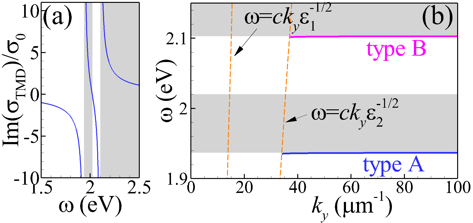
If TMD is cladded by two semi-infinite dielectric media with dielectric constants and , it is able to sustain surface EPs with a dispersion relation, , determined by the equation [14]
| (2) |
where and are out-of-plane and in-plane components of the wave vector, respectively, in the medium with dielectric constant , , and is the velocity of light in vacuum. Neglecting damping, and are purely imaginary for surface EPs, in contrast with the MC polaritons. As an example, the dispersion of surface EPs in a single layer of is depicted in Fig. 1(b). There are two such modes [type A and type B, depicted in Fig. 1(b) by solid blue and pink lines, correspondingly], which exist in the frequency ranges where imaginary part of TMD conductivity is negative (white domains in Fig. 1), as it happens for s-polarized plasmon-polaritons in graphene [17]. Notice that both A and B-type surface EP modes occur outside of the light cone, their dispersion curves bifurcate from the less steep light line, , and asymptotically approach the exciton transition frequencies, and , at large values of . Alike other evanescent waves, surface EPs cannot be excited directly by external propagating electromagnetic (EM) waves.
As mentioned above, the efficiency of the exciton-light coupling can be enhanced considerably if the TMD layer is placed in an optical resonance system, such as Fabry-Perot [11, 14], micropillar [10, 18] or Tamm-plasmon [12, 13] microcavity, on top of a specially prepared metasurface [15, 8] or just near a plasmonic surface [19]. In this way, the strong coupling regime can be achieved, which offers a range of potential applications (see references in the recent papers [8, 18]). The presence of a MC confining the light allows for the existence of the "bulk"-type MC polaritons with real , [20], which coexist with the surface EPs [14].
However, it may be not a MC but rather a heterostructure formed by two finite PCs (or Bragg reflectors, BR, in other words) where the latter type of modes exist. The existence of lossless electromagnetic (EM) interface modes at the boundary of such a heterostructure was demonstrated in Ref. [21], where they were named optical Tamm states; later the term passed to designate mostly localized (in one direction) EM modes formed in the gap between a BR and a metal surface, coupled to metal plasmons [22, 23, 24]. In this paper we demonstrate that a TMD monolayer embedded in a photonic crystal (PC) is able to sustain localized EP eigenstates, similar to other types of "defects" in PCs, which break the translational symmetry along the PC axis [25, 26, 27, 28, 29, 30]. These states are characterized by a well-defined real in-plane component of the -vector, i.e. they correspond to evanescent waves coupled to the TMD excitons. Such modes can be excited directly by external light if the number of periods in the PC is not too large. Moreover, using oblique incidence of light and measuring absorbance, one can probe the dispersion relation of these modes as demonstrated by our numerical simulation.
2 Electromagnetic eigenmodes
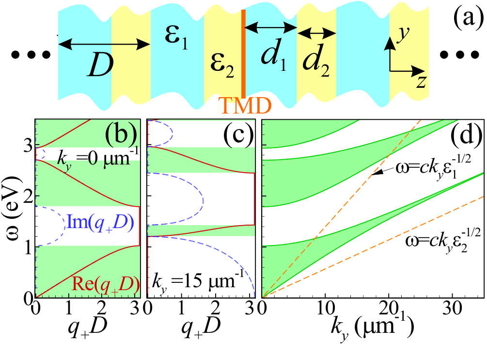
Let us consider a photonic crystal with a period , composed of two alternating dielectric layers [along -axis, see Fig. 2(a)], a layer with the dielectric constant and thickness (which occupies spatial domains ) and a layer with dielectric constant and thickness [arranged at spatial domains ]. Here stands for the PC cell’s number. We also suppose that the TMD layer is placed at the boundary between two dielectrics (plane ). If the EM field is uniform in -direction (), Maxwell’s equations for a TE-polarized wave (containing components , and ) read:
| (3) | |||
| (4) |
Here the spatial and temporal dependence of the EM field of the form is assumed. Notice that the composite superscript in Eqs. (3)–(4) is prescribed to the EM field components defined in the -th unit cell of the PC, in its part filled with the dielectric . After solving Maxwell’s equations in each slab and applying boundary conditions (see Supplemental Document for details), it is possible to relate the tangential components of the field across the PC period via the unit cell transfer matrix , i.e.,
| (9) |
The dispersion relation of electromagnetic waves in a perfect infinite PC can be obtained by applying the Bloch theorem. It can be represented in terms of eigenvalues, , and eigenvectors, , of the matrix (see Eq. (S2) of Supplemental Document). Namely, the following equation holds:
| (10) |
The eigenvalues, and , determine the dispersion relations for forward- and backward-propagating waves, respectively. Moreover, as the matrix is unimodular, the pair of eigenvalues possess the property , which implies the relation .
The Bloch wavevector can be either real or imaginary (if damping is neglected), which depends on whether the chosen pair of and belongs to the allowed or forbidden (also called stop-band) part of the PC’s spectrum. Namely, inside the allowed bands [green-shadowed domains in Figs. 2(b) and 2(c)], the Bloch wavevector of forward-propagating wave is purely real and positive, i.e., , . In contrast, inside the stop-bands [white domains in Figs. 2(b) and 2(c)], the Bloch wavevector can be treated as a complex value with the real part and a positive imaginary part . The latter implies the evanescent character of forward-propagating wave inside the stop-band and its decrease in the positive direction of -axis. Accordingly, for a backward-propagating wave inside the stop-band, i.e. its amplitude decreases in the negative direction of -axis.
Let us now turn to a PC intercalated by a TMD layer. The fields in each part of it, at planes with standing for an integer, either positive or negative, can be represented as follows (see Eq. (S3) of Supplemental Document):
Such a representation avoids the appearance of waves exponentially growing towards . Substituting these equations into boundary conditions across the TMD layer,
| (17) |
where
is the boundary condition matrix, it is possible to obtain the following (implicit) dispersion relation
| (19) |
for the localized eigenstate supported by TMD embedded into the PC (compare to Eq. (2)).
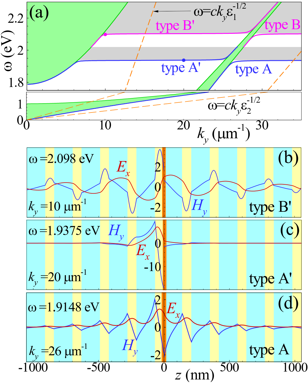
The spectrum of the perfectly periodic PC [see Fig. 2(d)] contains a low-frequency stop-band, which vanishes at (we shall call it “zeroth-order”), and higher order stop-bands whose width remains finite at . This fact is crucial for the existence of two different types of localized eigenstates supported by the inserted TMD layer, whose spectra are shown in Fig. 3(a). For the particular parameters of Fig. 3(a), the spectrum contains four distinct modes: (i) two (type A and type B) in the zeroth stop-band, and (ii) two (type A’ and type B’) within the first stop-band. The properties of the A and B modes are similar to those of the surface EPs supported by TMD cladded by two semi-infinite dielectrics, described by Eq. (2) and briefly discussed in the Introduction [see Fig. 1(b)]. Yet, there is one distinctive feature: in the PC, the A and B modes bifurcate from the edge of the first allowed band and can exist on the left of the less steep light line, .
The modes inside the first stop-band, named A’ and B’, have remarkably different properties. They do not approach asymptotically the exciton transition frequencies but rather cross them. Moreover, for large they occur in the frequency ranges where the imaginary part of TMD’s conductivity is positive (shadowed in Fig. 3(a)). In the frequency range far from and , is small and, as a result, the localized eigenstate appears close to the edge of the allowed band of the PC. At the same time, the spatial profile is rather weakly localized in the vicinity of the TMD layer (actually, the same happens to the "usual" surface EPs; examples are shown in Fig. 3(b) and 3(d) for the type B’ and type A modes, respectively). In contrast, for the frequencies near and , the absolute value of TMD’s conductivity is high. As a consequence, the localized eigenstate lies deeply inside the stop-band and its spatial profile is strongly localized [see Fig. 3(c)].
The A’ and B’ modes, lying within the gap of the PC crystal spectrum, possess another interesting property. Their dispersion curves lie (partially) on the left of the steepest of the two light lines of the dielectrics constituting the PC. Both facts are characteristic of the lossless optical Tamm states (OTS), first described for a heterostructure of two semi-infinite PCs [21]. If the two halves of the structure were identical, there would be no OTS unless the full translation symmetry is broken in some other way like introducing the TMD layer. It also leads to the coupling between the optical mode and the exciton and their anti-crossing as described for a conventional quantum well [31] and also for 2D semiconductors in a structure where one of the BRs was replaced by a metallic mirror [13]. The "primed" modes of Fig. 3 are weakly localized OTS-type modes with real Bloch wavevector and the frequency in the vicinity of the PC band edge. They become increasingly excitonic in nature as increases. We shall demonstrate it further in the next section.
3 Diffraction of light on a TMD-intercalated PC
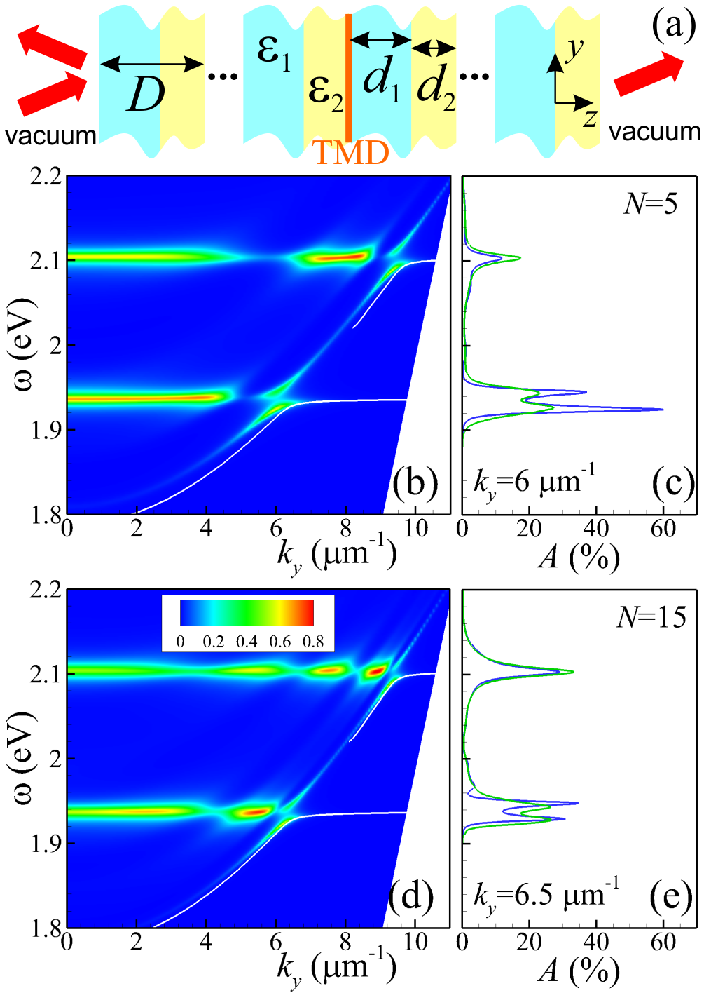
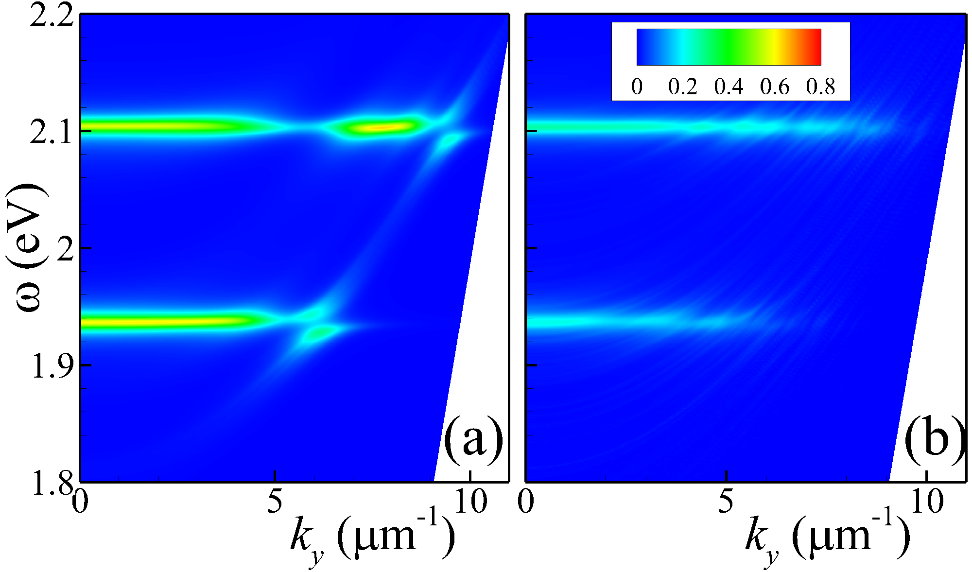
As discussed above, the localized eigenstates A’ and B’ lie on the left of the line and even the vacuum light line in some frequency range. It means that these modes can be coupled to external propagating EM waves, i.e. excited directly by light without using a prism or a grating. Let us consider a PC with a finite (and relatively small) number of periods, hosting the TMD layer. An example of such a structure is shown in Fig. 4(a) where the TMD layer is embedded into a truncated PC containing elementary cells intercalated with a TMD layer ( cells before and cells after the TMD layer). Light with frequency falls on the surface of the truncated PC at an angle of incidence , which determines the transverse wavevector component .
The amplitudes of the incident, , reflected, , and transmitted, , waves in such a truncated PC with the TMD layer inside can be related via the transfer-matrix of the whole structure, (see Supplemental Document for details), namely:
| (24) |
From this equation, the amplitudes of the reflected and transmitted waves can be expressed through the matrix elements of as follows:
| (25) |
The absorbance () of the structure can be calculated as the difference between the Poynting vectors’ -components corresponding to the incident, reflected and transmitted waves,
| (26) |
and is depicted in Figs. 4(b) and 4(c). In these plots, the maximal absorption points on the plane reveal the characteristic anti-crossings between the horizontal lines representing the A and B excitons and the OTS dispersion curve (accompanying the edge of the PC stop-band). They coincide with the dispersion curves of the A’ and B’ modes shown by white lines. The small discrepancy between them can be accounted for the photonic crystal truncation (compare Figs. 4(c) and 4(b), calculated for different ). The intensity of the excitonic absorption on the left of the avoided crossing point is modulated also due to the small number of periods in the PCs.
The localized eigenstates are clearly observed in the absorption spectra and can be probed by means of angle-resolved spectroscopy [13, 31] if the frequency and transverse wavevector matching conditions are fulfilled. When the incident light couples to the A’ or B’ eigenmodes, the incident energy is transferred into the latter and finally dissipated through the exciton in the TMD layer.
How robust are the reported phenomena against the factors that differ real-world things from theoretical models, such as e.g. fluctuations of the PC-constituting dielectric layers? We addressed this question by calculating the absorbance of TMD-intercalated PCs with Gaussian-distributed random thicknesses of the layers, and , with mean values and as for the perfect structure and standard deviations and (see Sec. 2A of Supplemental Document for details). These results are shown in Figs. 4(c) and 4(e), demonstrating that the absorbance of the disordered structure (green lines) is decreased compared to the truncated perfect PC (blue lines), for the A’ mode. At the same time, the modes’ anti-crossing is still visible for =2.5%. In the Supplemental Document, we present maps similar to panels (b) and (d) of Fig. 4, calculated for stronger disorder (=10%), which show that the avoided crossing cannot be resolved anymore. We also notice that it cannot be resolved for the B’ mode already with small fluctuations of layers’ thicknesses. Somewhat unexpectedly, the intensity of this mode is enhanced by the disorder.
4 Conclusions
We predicted theoretically the existence of two types of localized exciton-polariton eigenstates in 1D photonic crystal with embedded TMD layer. If the excitonic transition frequencies of the TMD layer lie within the first stop-band of the PC for zero transverse wavevector, the spectrum of localized EP states consists of: (i) two (A and B) modes in the zeroth-order stop-band, and (ii) two (A’ and B’) in the first stop-band. The properties of the modes (i) are similar to those of the surface EPs supported by a single TMD cladded by two semi-infinite dielectrics, while modes (ii) are related to the optical Tamm states [21, 22, 31], although the analogy is only partial in both cases.
The A’ and B’ modes result from the coupling of the TMD exciton to the Tamm-type state of light in the photonic crystal with the translational symmetry broken by the inserted TMD layer. Coupling of such a photonic state localized by two reflectors to elementary excitations in a 2D material has recently been described for the case of graphene plasmons [32]. The Tamm-type modes predicted here can be effectively coupled to propagating light waves falling directly on the surface of the PC with a relatively small number of unit cells. In the presented simulated example [Fig. 4(c)] we demonstrated the feasibility of excitation of such localized eigenstate in an experimentally attainable structure with the dielectric constants and , corresponding to a SiO2/Si3N4 BR used in Ref. [33] (these and other inexpensive dielectrics are commonly used for making reasonable Bragg reflectors [34]). Methods similar to the suggested experiment were already used [24, 31, 33] for demonstration of optical Tamm states, even though one of the BRs was replaced by another type of mirror, such as a metal or an organic dye film. Our simulations for the structure with natural disorder (fluctuations of layers’ thicknesses) demonstrate that the characteristic avoided crossing can be observed for the A’ mode if the relative dispersion of the thicknesses is below 5%. Therefore, we hope that this article may stimulate experiments aimed at observing this new type of localized exciton-polaritons.
Acknowledgements
Y.V.B., N.M.R.P., and M.I.V. acknowledge support from the European Commission through the project “Graphene-Driven Revolutions in ICT and Beyond”- Core 3 (Ref. No. 881603) and the Portuguese Foundation for Science and Technology (FCT) in the framework of the Strategic Funding UIDB/04650/2020. Authors also acknowledge FEDER and FCT for support through projects POCI-01-0145-FEDER-028114 and PTDC/FIS-MAC/28887/2017. The authors declare no conflicts of interest.
References
- Novoselov et al. [2004] K S Novoselov, A. K. Geim, S V Morozov, D Jiang, Y Zhang, S V Dubonos, I V Grigorieva, and A A Firsov. Electric Field Effect in Atomically Thin Carbon Films. Science, 306(5696):666–669, oct 2004. ISSN 1095-9203. doi:10.1126/science.1102896. URL http://arxiv.org/abs/cond-mat/0410550http://www.sciencemag.org/content/306/5696/666.abstract.
- Mak et al. [2010] Kin Fai Mak, Changgu Lee, James Hone, Jie Shan, and Tony F. Heinz. Atomically Thin MoS2: A New Direct-Gap Semiconductor. Physical Review Letters, 105(13):136805, sep 2010. ISSN 0031-9007. doi:10.1103/PhysRevLett.105.136805. URL https://link.aps.org/doi/10.1103/PhysRevLett.105.136805.
- Splendiani et al. [2010] Andrea Splendiani, Liang Sun, Yuanbo Zhang, Tianshu Li, Jonghwan Kim, Chi Yung Chim, Giulia Galli, and Feng Wang. Emerging photoluminescence in monolayer MoS2. Nano Letters, 10(4):1271–1275, 2010. ISSN 15306984. doi:10.1021/nl903868w.
- Arra et al. [2019] Srilatha Arra, Rohit Babar, and Mukul Kabir. Exciton in phosphorene: Strain, impurity, thickness, and heterostructure. Phys. Rev. B, 99:045432, Jan 2019. doi:10.1103/PhysRevB.99.045432. URL https://link.aps.org/doi/10.1103/PhysRevB.99.045432.
- He et al. [2014] Keliang He, Nardeep Kumar, Liang Zhao, Zefang Wang, Kin Fai Mak, Hui Zhao, and Jie Shan. Tightly Bound Excitons in Monolayer WSe2. Physical Review Letters, 113(2):026803, jul 2014. ISSN 0031-9007. doi:10.1103/PhysRevLett.113.026803. URL https://link.aps.org/doi/10.1103/PhysRevLett.113.026803.
- Ye et al. [2015] Yu Ye, Zi Jing Wong, Xiufang Lu, Hanyu Zhu, Xianhui Chen, Yuan Wang, and Xiang Zhang. Monolayer excitonic laser. Nature Photonics, 9:733, 2015.
- Liu et al. [2017] Jiang-Tao Liu, Hong Tong, Zhen-Hua Wu, Jin-Bao Huang, and Yun-Song Zhou. Greatly enhanced light emission of MoS2 using photonic crystal heterojunction. Scientific Reports, 7(1):16391, nov 2017. doi:10.1038/s41598-017-16502-2.
- Chen et al. [2020] Yueyang Chen, Shengnan Miao, Tianmeng Wang, Ding Zhong, Abhi Saxena, Colin Chow, James Whitehead, Dario Gerace, Xiaodong Xu, Su-Fei Shi, and Arka Majumdar. Metasurface integrated monolayer exciton polariton. Nano Letters, 20(7):5292–5300, 2020. doi:10.1021/acs.nanolett.0c01624. URL https://doi.org/10.1021/acs.nanolett.0c01624.
- Wang et al. [2018] Gang Wang, Alexey Chernikov, Mikhail M. Glazov, Tony F. Heinz, Xavier Marie, Thierry Amand, and Bernhard Urbaszek. Colloquium: Excitons in atomically thin transition metal dichalcogenides. Rev. Mod. Phys., 90:021001, 2018.
- Liu et al. [2015] Xiaoze Liu, Tal Galfsky, Zheng Sun, Fengnian Xia, Erh-chen Lin, Yi-Hsien Lee, Stéphane Kéna-Cohen, and Vinod M. Menon. Strong light-matter coupling in two-dimensional atomic crystals. Nature Photonics, 9(1):30–34, jan 2015. ISSN 1749-4885. doi:10.1038/nphoton.2014.304. URL http://dx.doi.org/10.1038/nphoton.2014.304http://www.nature.com/articles/nphoton.2014.304.
- Dufferwiel et al. [2015] S. Dufferwiel, S. Schwarz, F. Withers, A. A. P. Trichet, F. Li, M. Sich, O. Del Pozo-Zamudio, C. Clark, A. Nalitov, D. D. Solnyshkov, G. Malpuech, K. S. Novoselov, J. M. Smith, M. S. Skolnick, D. N. Krizhanovskii, and A. I. Tartakovskii. Exciton-polaritons in van der Waals heterostructures embedded in tunable microcavities. Nature Communications, 6(1):8579, dec 2015. ISSN 2041-1723. doi:10.1038/ncomms9579. URL http://www.nature.com/articles/ncomms9579.
- Flatten et al. [2016] L. C. Flatten, Z. He, D. M. Coles, A. A. P. Trichet, A. W. Powell, R. A. Taylor, J. H. Warner, and J. M. Smith. Room-temperature exciton-polaritons with two-dimensional ws2. Scientific Reports, 6:33134, 2016. doi:10.1038/srep33134. URL https://doi.org/10.1038/srep33134.
- Lundt et al. [2016] Nils Lundt, Sebastian Klembt, Evgeniia Cherotchenko, Simon Betzold, Oliver Iff, Anton V. Nalitov, Martin Klaas, Christof P. Dietrich, Alexey V. Kavokin, Sven Höfling, and Christian Schneider. Room-temperature tamm-plasmon exciton-polaritons with a wse2 monolayer. Nature Communications, 7:13328, 2016.
- Vasilevskiy et al. [2015] Mikhail I. Vasilevskiy, Darío G. Santiago-Pérez, Carlos Trallero-Giner, Nuno M. R. Peres, and Alexey Kavokin. Exciton polaritons in two-dimensional dichalcogenide layers placed in a planar microcavity: Tunable interaction between two Bose-Einstein condensates. Physical Review B, 92(24):245435, dec 2015. ISSN 1098-0121. doi:10.1103/PhysRevB.92.245435. URL https://link.aps.org/doi/10.1103/PhysRevB.92.245435.
- Zhang et al. [2018] Long Zhang, Rahul Gogna, Will Burg, Emanuel Tutuc, and Hui Deng. Photonic-crystal exciton-polaritons in monolayer semiconductors. Nature Communications, 9:713, 2018. doi:10.1038/s41467-018-03188-x. URL https://doi.org/10.1038/s41467-018-03188-x.
- Hu et al. [2019] F. Hu, Y. Luan, J. Speltz, D. Zhong, C. H. Liu, J. Yan, D. G. Mandrus, X. Xu, and Z. Fei. Imaging propagative exciton polaritons in atomically thin WSe2 waveguides. Physical Review B, 100(12):121301, sep 2019. ISSN 2469-9950. doi:10.1103/PhysRevB.100.121301. URL https://link.aps.org/doi/10.1103/PhysRevB.100.121301.
- Mikhailov and Ziegler [2007] Sergey A. Mikhailov and Klaus Ziegler. New Electromagnetic Mode in Graphene. Physical Review Letters, 99(1):016803, jul 2007. ISSN 0031-9007. doi:10.1103/PhysRevLett.99.016803. URL http://link.aps.org/doi/10.1103/PhysRevLett.99.016803https://link.aps.org/doi/10.1103/PhysRevLett.99.016803.
- Gomes et al. [2020] José Nuno S. Gomes, Carlos Trallero-Giner, Nuno M. R. Peres, and Mikhail I. Vasilevskiy. Exciton–polaritons of a 2d semiconductor layer in a cylindrical microcavity. Journal of Applied Physics, 127(13):133101, 2020. doi:10.1063/1.5143244.
- Gonçalves et al. [2018] P. A. D. Gonçalves, L. P. Bertelsen, Sanshui Xiao, and N. Asger Mortensen. Plasmon-exciton polaritons in two-dimensional semiconductor/metal interfaces. Physical Review B, 97(4):041402, jan 2018. ISSN 2469-9950. doi:10.1103/PhysRevB.97.041402. URL https://link.aps.org/doi/10.1103/PhysRevB.97.041402.
- Kavokin et al. [2008] A. V. Kavokin, J. J. Baumberg, G. Malpuech, and F. P. Laussy. Microcavities. Oxford University Press, Oxford, UK, 2008.
- Kavokin et al. [2005] A. V. Kavokin, I. A. Shelykh, and G. Malpuech. Lossless interface modes at the boundary between two periodic dielectric structures. Phys. Rev. B, 72:233102, Dec 2005. doi:10.1103/PhysRevB.72.233102. URL https://link.aps.org/doi/10.1103/PhysRevB.72.233102.
- Kaliteevski et al. [2007] M. Kaliteevski, I. Iorsh, S. Brand, R. A. Abram, J. M. Chamberlain, A. V. Kavokin, and I. A. Shelykh. Tamm plasmon-polaritons: Possible electromagnetic states at the interface of a metal and a dielectric bragg mirror. Phys. Rev. B, 76:165415, 2007. doi:10.1103/PhysRevB.76.165415. URL https://link.aps.org/doi/10.1103/PhysRevB.76.165415.
- Gazzano et al. [2012] O. Gazzano, S. Michaelis de Vasconcellos, K. Gauthron, C. Symonds, P. Voisin, J. Bellessa, A. Lemaître, and P. Senellart. Single photon source using confined tamm plasmon modes. Applied Physics Letters, 100(23):232111, 2012. doi:10.1063/1.4726117. URL https://doi.org/10.1063/1.4726117.
- Sasin et al. [2010] M. E. Sasin, R. P. Seisyan, M. A. Kaliteevski, S. Brand, R. A. Abram, J. M. Chamberlain, I. V. Iorsh, I. A. Shelykh, A. Y. Egorov, A. P. Vasil’ev, V. S. Mikhrin, and A. V. Kavokin. Tamm plasmon-polaritons: First experimental observation. Superlattices and Microstructures, 47:44–49, 2010. doi:10.1016/j.spmi.2009.09.003.
- Yablonovitch et al. [1991] E. Yablonovitch, T. J. Gmitter, R. D. Meade, A. M. Rappe, K. D. Brommer, and J. D. Joannopoulos. Donor and acceptor modes in photonic band structure. Physical Review Letters, 67(24):3380–3383, dec 1991. ISSN 0031-9007. doi:10.1103/PhysRevLett.67.3380. URL http://link.aps.org/doi/10.1103/PhysRevLett.67.3380%****␣tmd_phot_crys_arxiv.bbl␣Line␣250␣****https://link.aps.org/doi/10.1103/PhysRevLett.67.3380.
- Villeneuve et al. [1996] Pierre R. Villeneuve, Shanhui Fan, and J. D. Joannopoulos. Microcavities in photonic crystals: Mode symmetry, tunability, and coupling efficiency. Physical Review B, 54(11):7837–7842, 1996. ISSN 0163-1829. doi:10.1103/PhysRevB.54.7837. URL http://link.aps.org/doi/10.1103/PhysRevB.54.7837.
- Notomi et al. [2001] M Notomi, K Yamada, A Shinya, J. Takahashi, C Takahashi, and I Yokohama. Extremely Large Group-Velocity Dispersion of Line-Defect Waveguides in Photonic Crystal Slabs. Physical Review Letters, 87(25):253902, nov 2001. ISSN 0031-9007. doi:10.1103/PhysRevLett.87.253902. URL https://link.aps.org/doi/10.1103/PhysRevLett.87.253902.
- Kuramochi et al. [2006] Eiichi Kuramochi, Masaya Notomi, Satoshi Mitsugi, Akihiko Shinya, Takasumi Tanabe, and Toshifumi Watanabe. Ultrahigh- Q photonic crystal nanocavities realized by the local width modulation of a line defect. Applied Physics Letters, 88(4):041112, 2006. ISSN 00036951. doi:10.1063/1.2167801.
- Noda et al. [2000] Susumu Noda, Alongkarn Chutinan, and Masahiro Imada. Trapping and emission of photons by a single defect in a photonic bandgap structure. Nature, 407(6804):608–610, oct 2000. ISSN 00280836. doi:10.1038/35036532. URL http://www.ncbi.nlm.nih.gov/pubmed/11034204http://www.nature.com/doifinder/10.1038/35036532.
- Valligatla et al. [2015] Sreeramulu Valligatla, Alessandro Chiasera, Stefano Varas, Pratyusha Das, B. N. Shivakiran Bhaktha, Anna Łukowiak, Francesco Scotognella, D. Narayana Rao, Roberta Ramponi, Giancarlo C. Righini, and Maurizio Ferrari. Optical field enhanced nonlinear absorption and optical limiting properties of 1-D dielectric photonic crystal with ZnO defect. Optical Materials, 50:229–233, 2015. ISSN 09253467. doi:10.1016/j.optmat.2015.10.032. URL http://dx.doi.org/10.1016/j.optmat.2015.10.032.
- Symonds et al. [2009] C. Symonds, A. Lemaître, E. Homeyer, J. C. Plenet, and J. Bellessa. Emission of tamm plasmon/exciton polaritons. Applied Physics Letters, 95:151114, 2009.
- Silva and Vasilevskiy [2019] J. M. S. S. Silva and M. I. Vasilevskiy. Far-infrared tamm polaritons in a microcavity with incorporated graphene sheet. Opt. Mater. Express, 9(1):244–255, Jan 2019. doi:10.1364/OME.9.000244. URL http://www.osapublishing.org/ome/abstract.cfm?URI=ome-9-1-244.
- Núnez-Sánchez et al. [2016] S. Núnez-Sánchez, M. Lopez-Garcia, M. M. Murshidy, A. G. Abdel-Hady, M. Serry, A. M. Adawi, J. G. Rarity, R. Oulton, and W. L. Barnes. Excitonic optical tamm states: A step toward a full molecular-dielectric photonic integration. ACS Photonics, 3:743 – 748, 2016.
- Yepuri et al. [2020] Venkatesh Yepuri, R. S. Dubey, and Brijesh Kumar. Rapid and economic fabrication approach of dielectric reflectors for energy harvesting applications. Scientific Reports, 10:15930, 2020. doi:10.1038/s41598-020-73052-w. URL https://doi.org/10.1038/s41598-020-73052-w.
5 Localized polariton states in a photonic crystal intercalated by a transition metal dichalcogenide monolayer: supplemental document
5.1 Transfer matrix formalism for a perfect PC
The solutions of the Maxwell’s equations in each slab can be expressed via transfer-matrices,
| (29) |
as
for spatial domains and , respectively. The tangential components of the field across the PC’s period can be related via the product of the transfer-matrices, , Eq. (5) of the main text, which expresses the continuity of the tangential components of the field across the dielectrics’ boundaries.
Applying the Bloch theorem,
we obtain:
| (34) |
where is the 22 unity matrix and stands for the Bloch wavevector.
The dispersion relation of electromagnetic waves inside the PC, as well as the general solution of Eq. (34), can be represented in terms of eigenvalues, , and eigenvectors, , of the matrix . This relation, coming from the compatibility condition of Eq. (34), can be expressed as Eq.(6) of the main text. Notice that the matrix is unimodular, since so are the matrices .
Let us notice that it is possible to obtain a general expression for the EM field components at a distance from the plane equal to an integer number of periods as a superposition of forward- and backward-propagating waves, using the Bloch theorem and the eigenvectors,
| (39) |
where are the amplitudes of the respective waves. This relation is used in the main text.
5.2 Transmission of an EM wave through a truncated photonic crystal
5.2.1 Truncated perfect PC
To calculate the absorbance of a finite PC (consisting of unit cells) with an embedded TMD layer in the middle, shown in Fig. 4(a) of the main text, we apply sequentially Eqs. (5) and (7) of the main text and obtain the following relation between the fields at PC’s boundaries:
| (44) |
Outside of the truncated PC (in the regions with ) the solutions of Maxwell’s equations [(3) and (4) of the main text] can be represented in the matrix form as
| (49) | |||
| (54) |
Here the superscripts and () correspond to the electromagnetic fields in the spatial domain and , respectively; , , and stand for the amplitudes of the electric field’s -component of the incident, reflected, and transmitted waves, respectively, is -component of the wavevector in vacuum, and
| (57) |
is the field matrix. In Eqs. (49)–(54), the incident and transmitted waves are assumed to be forward-propagating, while the reflected wave is backward-propagating. Using the condition of continuity of the tangential components at boundaries , it is possible to obtain a relation between the amplitudes of the incident, transmitted, and reflected waves from Eqs. (44), (49), and (54), which yields the absorbance, Eq. (11) of the main text, where
| (58) |
is the transfer-matrix of the whole structure.
5.2.2 Impact of disorder
Let us now consider the wave transmission through a truncated PC where the thicknesses of the layers are random values. We shall assume that the probability density of the thickness () follows a Gaussian distribution of the form
| (59) |
where and stand for the mean value and the standard deviation, respectively. In order to calculate the -th realization of the absorbance, , random numbers, , obeying the distribution (59) were generated (), which were used to obtain the -th realization of the transfer-matrix of the whole structure:
| (60) |
This matrix (60) was inserted into Eq. (11) of the main text,
| (61) |
The average absorbance, , of the disordered structure was calculated as
| (62) |
where is the number of absorbance realizations.
The results are shown in Fig. 5 for two magnitudes of disorder. As seen from the figure, the mode anti-crossing is still visible for =2.5%, although the PC band edge is less sharp than in the case of truncated perfect PC [see Fig. 4(b) in the main text] owing the presence of disorder. At the same time, the anti-crossing disappears completely in the case of strong disorder, =10% [Fig. 5(b)].