Anisotropy and effective medium approach in the optical response of 2D material heterostructures
Abstract
2D materials offer a large variety of optical properties, from transparency to plasmonic excitation. They can be structured and combined to form heterostructures that expand the realm of possibility to manipulate light interactions at the nanoscale. Appropriate and numerically efficient models accounting for the high intrinsic anisotropy of 2D materials and heterostructures are needed. In this article, we retrieve the relevant intrinsic parameters that describe the optical response of a homogeneous 2D material from a microscopic approach. Well-known effective models for vertical heterostructure (stacking of different layers) are retrieved. We found that the effective optical response model of horizontal heterostructures (alternating nano-ribbons) depends of the thickness. In the thin layer model, well adapted for 2D materials, a counter-intuitive in-plane isotropic behavior is predicted. We confront the effective model formulation with exact reference calculations such as ab-initio calculations for graphene, hexagonal boron nitride (hBN), as well as corrugated graphene with larger thickness but also with classical electrodynamics calculations that exactly account for the lateral structuration.
I Introduction
The extraordinary optical and electromagnetic (EM) properties of two-dimensional (2D) materials have been broadly investigated from visible light to microwaves [1, 2, 3, 4], leading to developments in various domains such as photovoltaics [5, 6], biosensors [7, 8], superabsorbers [9, 10] and transparent conducting films [11, 5]. The description of the EM response of a single layer has been debated recently [12, 13, 14, 15, 16, 17, 18, 19, 20, 21] based on a thin film model which assigns an effective permittivity to a layer with a given thickness, or on a 2D model which sets a surface susceptibility or conductivity at the interface between two media [17, 16, 19].
It is clear that anisotropy is essential in the description of 2D materials. As an example, recent ellipsometry results on MoS2 and graphene have shown that the out-of-plane response plays a crucial role in their optical response [15, 19]. In particular, the comparison between the thin film and surface susceptibility models required this out-of-plane response to be carefully handled as the materials are not periodic in that direction [17, 21].
The stacking of 2D layers modifies their electronic properties as shown for the stacking order of multilayer graphene [22, 23, 24, 25] or for the transition from direct to indirect band gap for TMDs [26, 27]. These effects mainly occur close to the Fermi level and affect less the EM response in the visible or U.V. range. The stacking also results in long-range (electrostatic) interactions that modify the optical response in the absence of change in the electronic structure of the system [12, 21]. This long-range interaction should also be accounted for to retrieve the single-layer optical response from quantum simulation based on supercell techniques (periodic repetition of the single-layer separated with vacuum) [12].
The high number of possible heterostructures and their atomic complexity, as well as their intrinsic anisotropy, demand a robust but computationally tractable approach. Vertical heterostructures, the stacking of identical or different 2D layers, have been widely investigated in the last decade [28, 29, 9, 30, 31, 32, 33, 34, 35, 36], in particular with an effective medium approach [28, 37, 17]. However, the thickness range of validity for a thin film or surface susceptibility effective models has not been explored. On the other hand, horizontal heterostructures of single-layer materials have been less studied [38, 31, 35, 39] and the effective models have not been confronted to exact methods that account for the structuring.
In this paper, first, we investigate the validity of the effective model for vertical 2D heterostructures with a graphene-hBN bilayer and we explore the limits of this approach with respect to the number of layers. Second, turning to horizontal heterostructure, we show that the optical response of 2D materials nanoribbons are correctly described with a different effective model than thick ribbons and nanorods [35, 40]. In particular, we show that 2D materials horizontal heterostructures optically behave like a uniform uniaxial material, isotropic in the plane.
In section II, starting from a microscopic framework, we define surface susceptibilities of 2D materials which are independent of the thickness, both for in-plane and out-of-plane polarisation, retrieving in a microscopic approach, that includes among others smooth transitions between layers, the results obtained from a macroscopic point of view in [21]. On this basis, the effective models for vertical and horizontal heterostructures are retrieved. The reference numerical methods, with which effective model will be compared, are described in section III. First-principle quantum approach (time-dependent density functional theory - TDDFT) has been performed when the size of the system permits, e.g. for vertical heterostructure, and classical electrodynamics approach that exactly accounts for the structuring (Rigorous coupled wave analysis (RCWA)) has been used for horizontal heterostructure. In section IV we apply the effective models on various heterostructures and we compare the results with reference simulations. Graphene multilayers and a graphene-hBN bilayer are investigated for vertical heterostructures while graphene nanoribbons and graphene-hBN hetero-nanoribbons are studied for horizontal heterostructures.
II Effective Medium theory for 2D materials and heterostructures
In this section, macroscopic response functions are related to microscopic response functions and effective models are deduced for heterostructures.
II.1 The irreducible and external susceptibilities
The time dependencies of the potentials are supposed to be harmonic, i.e. . Below, this factor is not shown for the sake of conciseness. is a periodic potential with a uniform amplitude applied on a material at a microscopic (atomic) scale,
| (1) |
The induced and total potentials and can be written as follows:
| (2) | |||||
| (3) |
where the spatial variation of the functions and are related to the local fields (LF) and have the same spatial periodicity as the unit cell of the material. We define here the irreducible susceptibility and the external susceptibility by:
| (4) | ||||
| (5) |
where the integrals span over the whole space. These susceptibilities can be calculated from the more usual irreducible and external polarizabilities [41, 42]. The macroscopic dielectric function of a material is obtained through the average of the potential over the unit cell [43, 44, 45] :
| (6) |
Taking the average of the total potential from eq. (5) using the fact that the total field is the sum of the applied and the induced fields, it comes:
| (7) | ||||
| (8) |
with the volume of the unit cell. The macroscopic external susceptibility defined by eq. (8) relates the total displacement field to the polarization field
| (9) |
This susceptibility has already been defined in [21] as the displacement susceptibility. In contrast, the macroscopic irreducible susceptibility , the usual susceptibility of electromagnetism, is defined by
| (10) |
and is obtained from eq. (8),
| (11) |
In general cannot be obtained directly by averaging eq. (4), because of the spatial variations of the total field in the unit cell, associated with the local fields effect. However, if the material is homogeneous, the LF are negligible and the total field can be replaced by its spatial average in eq. (4) [43, 46] and
| (12) | ||||
| (13) |
where is equal to that obtained using eq. (11).
II.2 Permittivity and surface susceptibilities of 2D materials
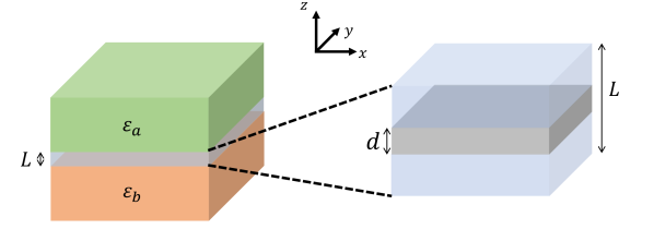
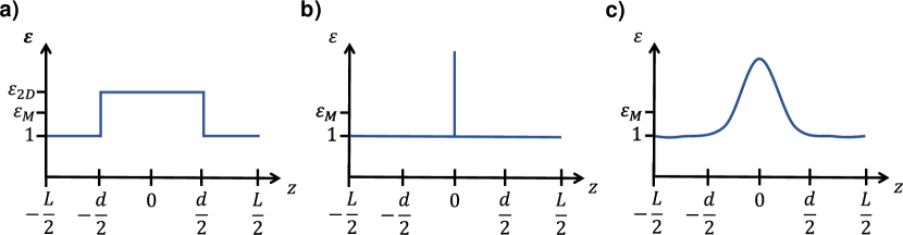
Bidimensional materials cannot be considered strictly 2D because the electronic wave function extends in the normal direction. Therefore, the microscopic dielectric function varies along this direction. In order to determine this permittivity both numerically (e.g. using TDDFT [12, 44]) and experimentally (e.g. using ellipsometry [47, 15, 19]), 2D materials can be modelled as a layer with a constant permittivity over a thickness [12, 44]. In the most general case, the layer of thickness is embedded between two media of different permittivities and as represented in fig. 1 (left). Following [21], this layer can be described as a 2D material of permittivity with thickness surrounded by vacuum (fig. 1, right). This vacuum may for example represent the vacuum layers of the supercell used in DFT, or the interlayer distance with another 2D material in the case of heterostructures. The spatial variation of the permittivity in this layered system (vacuum – 2D material – vacuum) is schematically represented in fig. 2. When , it corresponds to the thin film model. When , the 2D material is infinitely thin and the permittivity is represented using a Dirac distribution as for a finite surface polarization at the interface between two materials. These two approaches have been formally combined in [21]. Other models can be imagined such as a continuous permittivity, with a maximum value at the center of the atomic layer as represented in fig. 2c. However, we show in the following that at a macroscopic scale, all these descriptions are equivalent.
To rigorously define the surface susceptibilities of 2D materials, we use the effective model describing the three-layer system (vacuum – 2D material – vacuum) represented on the right side of fig. 1 and in fig. 2a. This effective model comes, for in-plane polarization, from the conservation over the whole system of the tangential component of the electric field, in which case we can use the parallel capacitors equation, eq. (S9). For out-of-plane polarization, it comes from the conservation of the normal component of the displacement field, in which case we can use the series capacitors equation eq. (S12) [41, 48, 49]. For in-plane polarization, it gives:
| (14) |
and for out-of-plane polarization
| (15) |
The permittivities and are the permittivities of the layer of thickness for in-plane and out-of-planes polarizations respectively.
The fact that the effective permittivity modelling is different for and directions is related to the role of the local field on the optical properties of stratified media and 2D materials. LF affects mostly fields polarized perpendicularly to the sheets, while it may be neglected for in-plane polarization [50, 12]. Since LFs are negligible for this polarization, of eq. (12) can be used to evaluate in eq. (14) and, with , we obtain
| (16) |
with the surface of the unit cell.
We can define the surface irreducible susceptibility for in-plane polarization of a 2D material as
| (17) |
such that
| (18) |
The second term of the right-hand side of eq. (16) is the average value of the microscopic susceptibility over a surface and a height . Therefore, it does not depend directly on the variation profile of the permittivity in the layer of thickness L or on the distance and the equation (18) is valid for other models such as those represented in fig. 2b and c. While the in-plane surface susceptibility is independent of the chosen thickness , as it accounts only for the response of the 2D material in the volume of thickness , we note that the effective permittivity depends on .
The same reasoning can be performed for the out-of-plane polarization. Because the LF cannot be neglected, eq. (8) is used to obtain the effective permittivity of the layer
| (19) |
As before, the second term of the right-hand side of eq. (16) is the average value of the microscopic susceptibility over a surface and a height . The surface external susceptibility for out-of-plane polarization is then
| (20) |
and the effective out-of-plane permittivity of the layer is
| (21) |
As for the in-plane response, the surface external susceptibility is independent of the thickness, but the effective permittivity depends on the thickness of the layer.
We emphasize, as stated above, that the surface susceptibilities of eqs. (17) and (20) are model-independent, in the sense that they do not depend on the exact variation profile of the permittivity (see fig. 2). They describe the average response of the 2D material at this interface and they are the relevant quantities to describe the optical response of 2D materials at a macroscopic scale. In particular, they are related to the surface polarization field by
| (22) |
and
| (23) |
Note that has been used to characterize the out-of-plane polarization of 2D materials [13, 17, 19, 20]. However, from eq. (11), we see that it is not an intrinsic quantity as it depends on the thickness L.
| (24) |
Moreover, when the constitutive relation is used instead of eq. (23), the obtained surface response function are found to problematically depend on the surrounding media [13, 17, 19, 20]. In the case of a 2D layer in vacuum or when the out-of-plane susceptibility is neglected, the derived optical responses are not affected. But recent ellipsometry measurements on graphene and MoS2 in the visible range [19] cannot be interpreted with a model that neglects the out-of-plane response of the 2D material, reinforcing the need to define truly intrinsic quantities for the 2D layer, independent of the external media [21].
The microscopic susceptibilities of 2D materials can be obtained numerically ab initio for a periodic system in a supercell approach [45, 46], with a vacuum layer of a few nanometers separating repeating layers to avoid short-range interactions between them. The thickness then corresponds to the height of the supercell. If, in the ab initio codes, the macroscopic permittivity is directly given as the result of the quantum calculations, the surface susceptibilities can be derived from eq. (18) and (21). The permittivities or susceptibilities can then be used in classical electrodynamics approaches, implementing each 2D material with a 2D or 3D model.
II.3 Effective model for 2D-material heterostructures
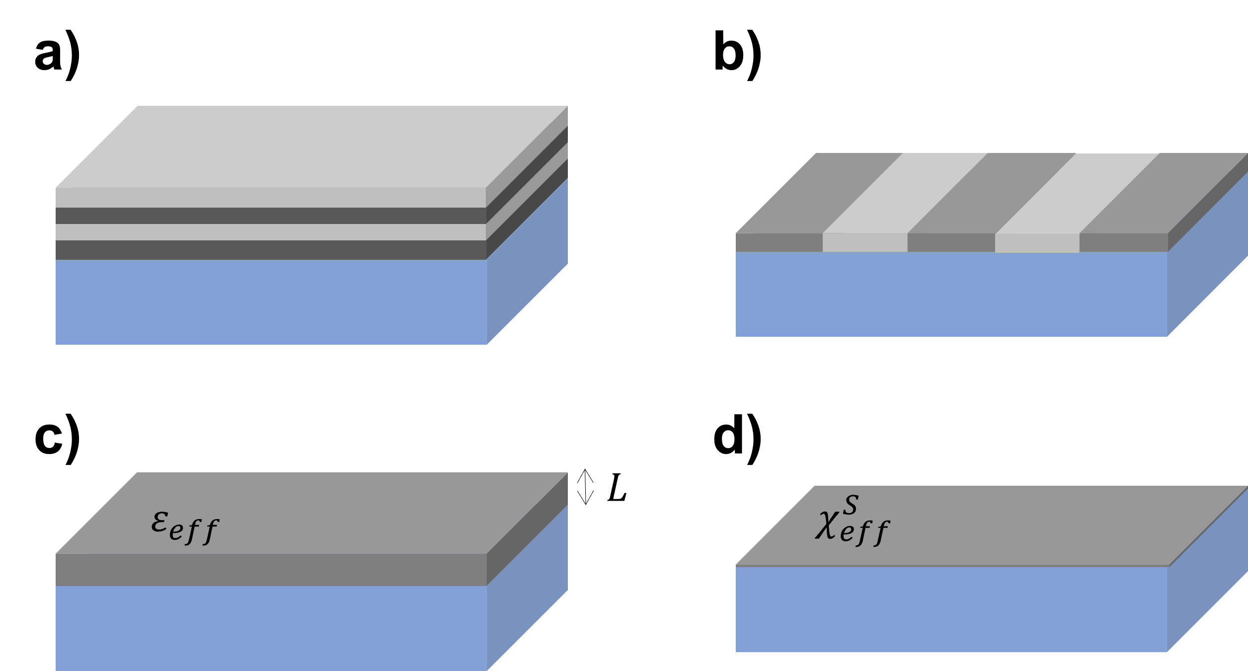
In this section, the in-plane and out-of-plane surface susceptibilities of horizontal and vertical heterostructures are related to the bulk effective permittivities of a thin film of finite thickness or to the surface susceptibilities of a surface polarization as shown in fig. 3, where (a) and (b) represent the heterostructures and (c) and (d) the effective models (3D or 2D).
II.3.1 Effective model for vertical heterostructures
A vertical heterostructure is modelled here as alternating layers of 2D materials and vacuum (fig. 3a), which can be seen as a generalisation of the approach of the previous section. The effective permittivity of a multilayer can be found using the parallel capacitors equation (eq. (S9)) [28, 37]. Moreover, the effective surface irreducible susceptibility of a purely 2D material equivalent to the multilayer can be deduced from eq. (S9) using eq. (18):
| (25) |
where the sum spans on each layer indexed . A further analysis of the validity of this approach is proposed in [21].
II.3.2 Effective model for lateral heterostructures
A horizontal heterostructure corresponds to alternating ribbons of 2D materials (fig. 3b). This kind of geometry was not considered in [21] and no model published up to now can provide the counter-intuitive results that are obtained for thin ribbons below.
Following the same approach as for vertical heterostructure, the effective susceptibilities of thick ribbons are found, reproducing well-known results [51, 35]:
| (27) |
| (28) |
where is the volume filling fraction of each type of ribbon.
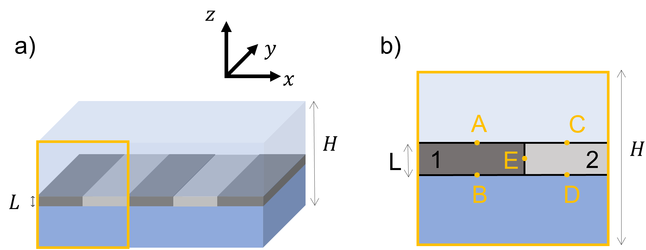
In the case of 2D materials, particular care must be taken owing to their extremely small thicknesses. We first consider the displacement field and the electric field in a unit cell composed of two distinct materials (fig. 4a, yellow rectangle). The incident medium and substrate have large thicknesses compared to the thickness of the 2D ribbon . The total thickness of the system, noted , verifies the condition .
If the electric field is polarized along the ribbon and parallel to the interface (i.e. along the -axis), it is conserved at the interfaces (namely at points , , , and depicted in fig. 4b). Therefore, as the wavelength of the field is much larger than , the electric field is uniform over the whole structure, which is the condition to apply the parallel capacitors equation eq. (S9) (see [41]). Accordingly, the effective susceptibility of the layer is
| (29) |
similarly to eq. (28) with the subscript indicating that this equation is valid for 2D materials.
When the electric field is polarized across the ribbon in the material plane (-axis), the electric field () is conserved at the interface at points , , and . At point , the displacement field normal to the surface is conserved and the electric field is discontinuous. Therefore, neither the electric field nor the displacement field are constant over the whole structure. The formal conditions to apply strictly the parallel or series capacitors equations are then not fulfilled.
Nonetheless, as the thickness of each ribbon is much smaller than its width, one can consider that the electric field does not vary between and (or between and ). Only close to the interface between the ribbons does the field vary truly. Consequently, in a first approximation, we consider the electric field constant over the two ribbons, neglecting the variation in the small volume around the interface between the two ribbons. The parallel capacitors equation eq. (S9) applies and:
| (30) |
which gives the same expression than the effective susceptibility in the polarization (if the 2D materials are isotropic in the plane). The 2D heterostructure is then isotropic in the 2D plane. This is a counter-intuitive result. This conclusion is also different from the one obtained for thick heterostructures (eq. (27)) that has been used in previous works on 2D materials [51, 35]. We will numerically analyse further these results later in the paper.
Finally, for electric fields across the 2D materials (along the -axis), the displacement field normal to the interface is conserved at the interfaces , , , but not , where the electric field parallel to the interface is conserved. As in the previous case, the displacement field can be approximated as being constant across the ribbons equation, thus (S12) leads to:
| (31) |
As for the direction, this is not the same result as for the thick ribbon effective model, which will also be numerically tested later in the paper.
This effective model for horizontal heterostructures is valid even for ribbon widths of the same order of magnitude as the wavelength. The only necessary condition is that this width needs to be much larger than the layer thickness such that the fields vary slightly in the ribbon.
As a consequence of the in-plane isotropy of the effective model, the optical response of such structured 2D materials at normal incidence does not depend on the polarization except if there are features that cannot be captured by the effective model. For instance, as surface plasmon resonances are phenomena appearing due to the structuring of the material, they cannot be described by the effective layer model. Therefore, comparing the spectra of the effective system to the proper system and inspecting the discrepancies can highlight the plasmonic resonances taking place in the ribbons.
III Numerical methods
In this section, we describe the reference numerical methods employed to illustrate the range of applicability of the surface susceptibilities and the effective models presented in section II.3. An ab initio atomistic method is used to determine the susceptibilities of 2D materials and of vertical heterostructures. The optical response is then obtained using the surface susceptibility model of a vertical heterostructure. On the other hand, a classical electrodynamic method is used to determine the absorption of horizontal heterostructures based on the susceptibilities of the individual components. In the last case, ab initio approaches are not feasible due to the large number of atoms in the unit cell but the horizontal structuring of the materials is fully accounted for, as well as the anisotropy. Those two methods are then complementary in order to verify the relevance of the effective models.
III.1 Time-dependent density functional theory (TDDFT)
The surface susceptibility of graphene, hBN and a bilayer graphene-hBN has been calculated using the GPAW implementation of TDDFT [52], within the random-phase approximation. Highly corrugated graphene with a thickness larger than a single layer of flat graphene was also investigated for comparison. The height of the unit cell of graphene and hBN is nm. For the bilayer, the graphene and hBN layers were separated by nm of vacuum, which corresponds to the interlayer distance in graphene and is close to the average interlayer distance of graphene-hBN heterostructures accounting for van der Waals corrections [53]. In this case, the total height of the cell is nm. The ground states of graphene, hBN, and the bilayer were calculated using a GGA-PBE functional [54], a k-point grid of and an energy cut-off of eV. For the TDDFT calculation, a cut-off energy of 250 eV was used. Corrugated graphene is modelled using a unit cell containing 50 atoms forming a hill of height nm in a cell of height nm as described in [55]. Its ground state is calculated using the LDA, a k-point grid and a cut-off energy of 400 eV. The cut-off energy for the TDDFT calculation is 20 eV. The GW and BSE calculations are not performed due to computational limitations, which could result in inaccurate optical spectra [56]. However, as we focus here on the effect of the anisotropy on the optical response of heterostructures, we ensure that the same level of approximation is considered when comparing systems. The link between microscopic and macroscopic response functions and effective quantities remains valid for all level of approximations.
III.2 Rigorous coupled wave analysis
A homemade code based on the rigorous coupled wave analysis (RCWA) method [57] was used. The RCWA method solves Maxwell equations for a series of layers of finite thicknesses with lateral structuring, as horizontal heterostructure. The method was adapted to account for the intrinsic anisotropy of materials in order to accurately model 2D materials [41]. The RCWA approach was used for modelling thin films and ribbons, with the dielectric functions obtained by TDDFT.
The thicknesses of the layers representing the 2D materials (structured or not) were arbitrarily fixed to nm for monolayer, or nm for bilayers. As long as these thicknesses are coherent with the thicknesses used to obtained the effective permittivity the results are independent of this choice [17].
IV Results and discussions
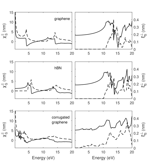
The surface susceptibilities of graphene and hBN are shown on fig. 5. It was first verified that and are independent of the supercell thickness (not shown). For the in-plane susceptibility (fig. 5, left panels) we observe the and the plasmons around respectively and eV, as expected without the GW and BSE correction [58]. The GW correction tends to blueshift the plasmon energy and the BSE one has the inverse effect. Together they produce a global blueshift of less than eV [59, 60, 61, 18]. The imaginary part of the out-of-plane susceptibility , responsible for the absorption, is exactly zero below eV, fig. 5, right panels. For corrugated graphene, the out-of-plane susceptibility is not negligible below eV, due to the atomic structure extending in the normal direction. This highlights the role of the valence bounds in the normal direction to the out-of-plane response of 2D materials.
The absorption spectra of the systems described by an effective surface polarization were obtained following the method published in our previous papers [17, 21]. It was adapted to incorporate the surface external susceptibility for the out-of-plane polarization [21]. The absorption spectra of the thin films and the ribbons were obtained using the RCWA method.
For all the following absorption calculations of 2D materials, the incident medium is air () and the refractive index of the substrate is . The angle of incidence is fixed to 70° in TM polarization to probe the effects of the anisotropy.
IV.1 Vertical heterostructures
We consider two types of vertical heterostructures. First, a system with identical layers (graphene) to analyse the limits of the 2D model compared to the thin film model. These structures may be synthesized experimentally up to a few layers using the transfer techniques on CVD-grown graphene for example [47]. Secondly, we test the validity of the effective model for vertical heterostructure (section II.3.1) on a graphene-hBN bilayer, whose optical properties have already been reported for in-plane polarizations [60, 32, 33].
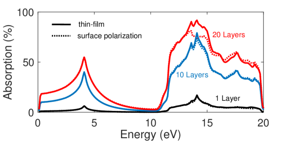
In fig. 6 the absorption of a single sheet of graphene (black), a multilayer of 10 sheets (blue) and a multilayer of 20 sheets of graphene (red) are calculated using the thin film model (solid lines) and the surface polarization model (dotted lines), showing the robustness of the strictly 2D model, even for 10 layers. For 20 layers, the discrepancies between the models become significant at high energy, in particular around the plasmon. In this case, the wavelength of the electromagnetic wave inside the layer is no longer larger than the thickness , and the phase shift cannot be neglected, which was an assumption for the 2D model. However, this result shows that the 2D model is not restricted to single-layered 2D materials and that few-layered 2D materials and heterostructures can also be modelled as surface polarization. The maximum number of layers is determined by the small-phase shift conditions and thus does not depend only on the thickness of the 2D material but also on its permittivity.
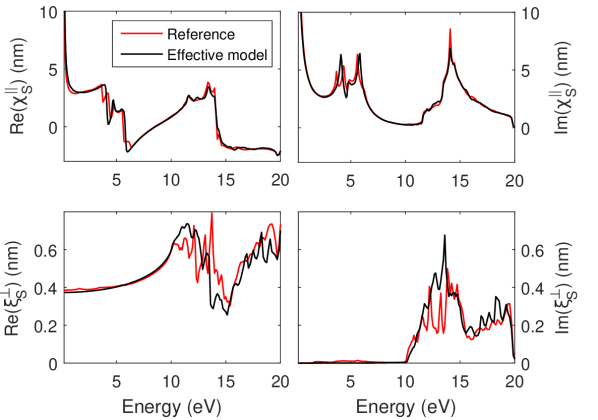
In fig. 7, the TDDFT surface susceptibilities (the reference) of a graphene-hBN bilayer are compared to the effective susceptibilities of eq. (25) and (26), with the single layers susceptibilities also obtained by TDDFT. The effective model replicates well except around eV which suggests a coupling between the -plasmons in each 2D material. For , the effective model fails to reproduce the TDDFT result above eV, though the global trend is conserved. This is due to long range electronic interactions that are significant even with large vacuum layers for out-of-plane polarization, as highlighted in [12].
IV.2 Horizontal heterostructure
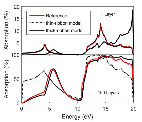
The first structure that we consider in this section is made of a 2D pattern alternating between graphene nanoribbons ( nm wide) and vacuum ( nm), leading to a filling factor of . To assess the domain of validity of the thin-ribbon (eqs. (29)-(31)) and thick-ribbon models (eqs. (27) and (28)), we compare a single-layer ribbon to a stack of ribbons, with a total thickness of nm.
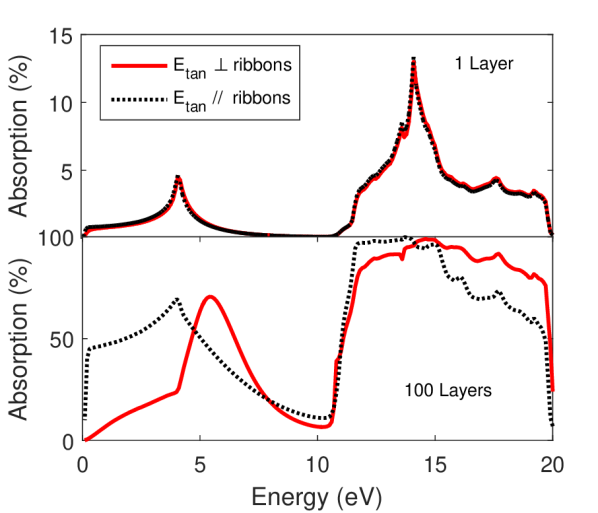
Using the RCWA method, the absorption of the graphene nanoribbons is obtained for two polarizations of the light with an incident angle of °, namely for the component of the electric field in the surface plane either parallel or perpendicular to the ribbons (fig. 8). To the best of our knowledge, this is the first investigation of 2D materials nanoribbons fully accounting for the intrinsic anisotropy of the 2D material. While for a large thickness (100 layers), the absorption depends on the polarisation, the aligned 2D nanoribbons have an isotropic response. To confirm this result, we also have considered an incident light with a different azimuthal angle, for which the tangential component of the electric field is neither parallel nor perpendicular to the ribbons. No modification of the polarization of the transmitted light has been observed, confirming the isotropy of the system. The uniaxial response of the thin horizontal heterostructure that our effective medium model has evidenced is then confirmed by the RCWA calculation, which fully describes the horizontal structure of the system.
For thick layers, the effective model (section II.3) predicts that this uniaxial character disappears and, consequently, when is perpendicular to the ribbon, the thick and thin ribbon effective models should differ. In fig. 9, the reference RCWA simulations are compared to the thin-ribbon and the thick-ribbon effective approaches for a single layer of graphene (top) and for a multilayer of 100 sheets of graphene (bottom). The thin-ribbon model reproduces perfectly the reference results for ribbons of a single sheet of 2D materials while the thick-ribbon model reproduces better the results for the large multilayer. Inversely the thick-ribbon model, which has sometimes been used for 2D materials, gives inaccurate results for single-layer 2D materials [51, 35].
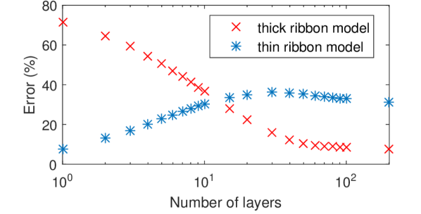
To better understand the transition between the two models, fig. 10 displays the relative error between each effective model and the reference (here the RCWA results) in function of the number of layers. This error is calculated as the normalized area between the curves of absorption :
| (32) |
with the incident energy. It confirms that, as shown before, the thin ribbon model is accurate for very few layers but the thick ribbon model works better for several tens of layers. In between, for 3 to 30 layers, the error is above 15% for both models and a full description of the system is necessary. As mentioned in section II.3, this result is also valid for larger ribbons, as the effective model only depends on the filling factor, as was verified numerically up to a width of nm (not shown).
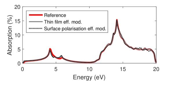
We now investigate a lateral repetition of graphene and hBN nanoribbons with of nm and nm width, respectively. These nanoribbons, have already been produced using CVD and etching device [62, 63], and may sustain plasmons [64, 39], which could be detected by comparison between the results of the effective model and the RCWA calculation. In fig. 11, the three models are compared: the reference model, the effective thin-film model and the effective surface polarization model. The three models agree almost perfectly, except at two specific energies. Around eV, the two effective models fail to reproduce the details of the RCWA results because of the plasmonic resonance that cannot be captured by effective models. This discrepancy was not observed in the graphene-air system which suggests that this plasmon originates from a coupling between the -plasmon of graphene and that of hBN, similarly to the case of vertical heterostructures. At high energy, above eV, the RCWA and the effective thin film model results are similar but the surface polarization model slightly differs. In this range, the wavelength is so small that the small phase shift approximation is not valid anymore, invalidating the strictly 2D model.
V Conclusions
We have proposed an original approach to develop effective models for vertical and horizontal heterostructures of 2D materials, based on the formal link between the microscopic and macroscopic description of the response functions of the materials. The importance of using two different surface susceptibilities, the irreducible susceptibility and the external susceptibility , defined independently from an arbitrary thickness of the layer, has been highlighted. In particular, it makes it possible to avoid the embarrassing definition of a surface response function that depends on the dielectric properties of the surrounding media.
It is only recently that experimental optical characterisation highlighted the role of out-of-plane susceptibility () for a coherent interpretation of the measurements [19]. It will become even more important with the rapid development of the study of heterostructures. This anisotropy could be taken into account together with the structuration of the material, as in the RCWA methods or in an effective medium approach. In some cases, the out-of-plane response can be neglected as for example, at normal incidence. Also, below eV, the imaginary part of is negligible for graphene and hBN while the real part is constant. As most of the optical features (absorption, plasmonic excitations,…) depend mainly on the imaginary part of , the optical spectra are weakly dependent on the out-of-plane response. This justifies a posteriori the use of models without out-of-plane responses in many previous research [10, 47, 65, 66].
For vertical heterostructures, we recovered the well-described effective medium model and expressed it in terms of the susceptibilities. With this effective approach, we reproduce quantitatively calculations from TDDFT although special care must be taken for plasmonic resonance and long-range interactions for out-of-plane polarization. We also demonstrated that the vertical heterostructure effective approach is robust up to tens of layers of graphene (more generally as far as the phase shift of the EM fields is negligible in the heterostructure).
The counter-intuitive uniaxial response of thin alternating nano-ribbons (horizontal heterostructures) is an unexpected outcome of the effective medium approach based on the surface susceptibilities. We successfully confront these predictions with RCWA numerical investigations and illustrate the transition towards an anisotropic behavior as the thickness increases (thick-layer model). This led to the description of an effective model for ribbons of 2D materials different from the effective model for thick ribbons or nanorods. In practice, the validity of the thin-layer model is already questioned for three-layer systems. In both cases, interface excitations, such as surface plasmons, cannot be captured by effective model approaches. As the RCWA method for horizontal heterostructure is numerically very efficient, a full description of the heterostructure rather than an effective medium approach is recommended to avoid questioning the limit of validity. However, the accurate description of systems composed of different 2D materials by a simple homogeneous thin film or surface current presents the obvious advantage of its simplicity and allows to analyse experimental data without numerical effort.
Acknowledgements.
This research used resources of the “Plateforme Technologique de Calcul Intensif (PTCI)” (http://www.ptci.unamur.be) located at the University of Namur, Belgium, which is supported by the FNRS-FRFC, the Walloon Region, and the University of Namur (Conventions No. 2.5020.11, GEQ U.G006.15, 1610468, RW/GEQ2016 et U.G011.22). The PTCI is a member of the “Consortium des Équipements de Calcul Intensif (CÉCI)”.References
- Rouhi et al. [2012] N. Rouhi, S. Capdevila, D. Jain, K. Zand, Y. Y. Wang, E. Brown, L. Jofre, and P. Burke, Terahertz graphene optics, Nano Res. 5, 667 (2012).
- Grigorenko et al. [2012] A. N. Grigorenko, M. Polini, and K. S. Novoselov, Graphene plasmonics, Nat. Photonics 6, 749 (2012).
- Bozzi et al. [2015] M. Bozzi, L. Pierantoni, and S. Bellucci, Applications of Graphene at Microwave Frequencies, Radioengineering 24, 661 (2015).
- Low and Avouris [2014] T. Low and P. Avouris, Graphene Plasmonics for Terahertz to Mid-Infrared Applications, ACS Nano 8, 1086 (2014), arXiv:1403.2799 .
- Park et al. [2012] H. Park, P. R. Brown, V. Bulović, and J. Kong, Graphene As Transparent Conducting Electrodes in Organic Photovoltaics: Studies in Graphene Morphology, Hole Transporting Layers, and Counter Electrodes, Nano Lett. 12, 133 (2012).
- Das et al. [2019] S. Das, D. Pandey, J. Thomas, and T. Roy, The Role of Graphene and Other 2D Materials in Solar Photovoltaics, Adv. Mater. 31, 1 (2019).
- Justino et al. [2017] C. I. Justino, A. R. Gomes, A. C. Freitas, A. C. Duarte, and T. A. Rocha-Santos, Graphene based sensors and biosensors, TrAC Trends Anal. Chem. 91, 53 (2017).
- Chattopadhyay et al. [2015] S. Chattopadhyay, M.-S. Li, P. Kumar Roy, and C. T. Wu, Non-enzymatic glucose sensing by enhanced Raman spectroscopy on flexible ‘as-grown’ CVD graphene, Analyst 140, 3935 (2015), arXiv:arXiv:1310.8002v1 .
- Batrakov et al. [2015] K. Batrakov, P. Kuzhir, S. Maksimenko, A. Paddubskaya, S. Voronovich, P. Lambin, T. Kaplas, and Y. Svirko, Flexible transparent graphene/polymer multilayers for efficient electromagnetic field absorption, Sci. Rep. 4, 7191 (2015).
- Lobet et al. [2016] M. Lobet, B. Majerus, L. Henrard, and P. Lambin, Perfect electromagnetic absorption using graphene and epsilon-near-zero metamaterials, Phys. Rev. B 93, 235424 (2016).
- Kasry et al. [2010] A. Kasry, M. A. Kuroda, G. J. Martyna, G. S. Tulevski, and A. A. Bol, Chemical Doping of Large-Area Stacked Graphene Films for Use as Transparent, Conducting Electrodes, ACS Nano 4, 3839 (2010).
- Tancogne-Dejean et al. [2015] N. Tancogne-Dejean, C. Giorgetti, and V. Véniard, Optical properties of surfaces with supercell ab initio calculations: Local-field effects, Phys. Rev. B - Condens. Matter Mater. Phys. 92, 1 (2015).
- Matthes et al. [2016] L. Matthes, O. Pulci, and F. Bechstedt, Influence of out-of-plane response on optical properties of two-dimensional materials: First principles approach, Phys. Rev. B 94, 205408 (2016).
- Merano [2016] M. Merano, Fresnel coefficients of a two-dimensional atomic crystal, Phys. Rev. A 93, 013832 (2016).
- Jayaswal et al. [2018] G. Jayaswal, Z. Dai, X. Zhang, M. Bagnarol, A. Martucci, and M. Merano, Measurement of the surface susceptibility and the surface conductivity of atomically thin MoS 2 by spectroscopic ellipsometry, Opt. Lett. 43, 703 (2018).
- Li and Heinz [2018] Y. Li and T. F. Heinz, Two-dimensional models for the optical response of thin films, 2D Mater. 5, 10.1088/2053-1583/aab0cf (2018).
- Majérus et al. [2018a] B. Majérus, E. Dremetsika, M. Lobet, L. Henrard, and P. Kockaert, Electrodynamics of two-dimensional materials: Role of anisotropy, Phys. Rev. B 98, 125419 (2018a).
- Guilhon et al. [2019] I. Guilhon, M. Marques, L. K. Teles, M. Palummo, O. Pulci, S. Botti, and F. Bechstedt, Out-of-plane excitons in two-dimensional crystals, Phys. Rev. B 99, 161201 (2019).
- Xu et al. [2021] Z. Xu, D. Ferraro, A. Zaltron, N. Galvanetto, A. Martucci, L. Sun, P. Yang, Y. Zhang, Y. Wang, Z. Liu, J. D. Elliott, M. Marsili, L. Dell’Anna, P. Umari, and M. Merano, Optical detection of the susceptibility tensor in two-dimensional crystals, Commun. Phys. 4, 215 (2021).
- Dell’Anna et al. [2022] L. Dell’Anna, Y. He, and M. Merano, Reflection, transmission, and surface susceptibility tensor of two-dimensional materials, Phys. Rev. A 105, 053515 (2022).
- Majérus et al. [2023] B. Majérus, L. Henrard, and P. Kockaert, Optical modeling of single and multilayer two-dimensional materials and heterostructures, Phys. Rev. B 107, 45429 (2023).
- Latil and Henrard [2006] S. Latil and L. Henrard, Charge Carriers in Few-Layer Graphene Films, Phys. Rev. Lett. 97, 036803 (2006).
- Cao et al. [2018] Y. Cao, V. Fatemi, S. Fang, K. Watanabe, T. Taniguchi, E. Kaxiras, and P. Jarillo-Herrero, Unconventional superconductivity in magic-angle graphene superlattices, Nature 556, 43 (2018).
- Yelgel [2016] C. Yelgel, Electronic Structure of ABC-stacked Multilayer Graphene and Trigonal Warping:A First Principles Calculation, J. Phys. Conf. Ser. 707, 12022 (2016).
- Hagymási et al. [2022] I. Hagymási, M. S. M. Isa, Z. Tajkov, K. Márity, L. Oroszlány, J. Koltai, A. Alassaf, P. Kun, K. Kandrai, A. Pálinkás, P. Vancsó, L. Tapasztó, and P. Nemes-Incze, Observation of competing, correlated ground states in the flat band of rhombohedral graphite, Sci. Adv. 8, eabo6879 (2022).
- Mann et al. [2014] J. Mann, Q. Ma, P. M. Odenthal, M. Isarraraz, D. Le, E. Preciado, D. Barroso, K. Yamaguchi, G. Von Son Palacio, A. Nguyen, T. Tran, M. Wurch, A. Nguyen, V. Klee, S. Bobek, D. Sun, T. F. Heinz, T. S. Rahman, R. Kawakami, and L. Bartels, 2-Dimensional transition metal dichalcogenides with tunable direct band gaps: MoS2(1-x)Se2x monolayers, Adv. Mater. 26, 1399 (2014).
- Kadantsev and Hawrylak [2012] E. S. Kadantsev and P. Hawrylak, Electronic structure of a single MoS 2 monolayer, Solid State Commun. 152, 909 (2012).
- Poddubny et al. [2013] A. Poddubny, I. Iorsh, P. Belov, and Y. Kivshar, Hyperbolic metamaterials, Nat. Photonics 7, 948 (2013).
- Bludov et al. [2013] Y. V. Bludov, N. M. R. Peres, and M. I. Vasilevskiy, Unusual reflection of electromagnetic radiation from a stack of graphene layers at oblique incidence, J. Opt. 15, 114004 (2013).
- Novoselov et al. [2016] K. S. Novoselov, A. Mishchenko, A. Carvalho, and A. H. Castro Neto, 2D materials and van der Waals heterostructures, Science (80-. ). 353, 10.1126/science.aac9439 (2016).
- Li et al. [2017] F. Li, W. Wei, P. Zhao, B. Huang, and Y. Dai, Electronic and Optical Properties of Pristine and Vertical and Lateral Heterostructures of Janus MoSSe and WSSe, J. Phys. Chem. Lett. 8, 5959 (2017).
- Wang et al. [2017] J. Wang, F. Ma, W. Liang, R. Wang, and M. Sun, Optical, photonic and optoelectronic properties of graphene, h-NB and their hybrid materials, Nanophotonics 6, 943 (2017).
- Farmani et al. [2017] A. Farmani, M. Yavarian, A. Alighanbari, M. Miri, and M. H. Sheikhi, Tunable graphene plasmonic Y-branch switch in the terahertz region using hexagonal boron nitride with electric and magnetic biasing, Appl. Opt. 56, 8931 (2017).
- Ren et al. [2019] K. Ren, M. Sun, Y. Luo, S. Wang, Y. Xu, J. Yu, and W. Tang, Electronic and optical properties of van der Waals vertical heterostructures based on two-dimensional transition metal dichalcogenides: First-principles calculations, Phys. Lett. Sect. A Gen. At. Solid State Phys. 383, 1487 (2019).
- Li et al. [2020] P. Li, G. Hu, I. Dolado, M. Tymchenko, C.-W. Qiu, F. J. Alfaro-Mozaz, F. Casanova, L. E. Hueso, S. Liu, J. H. Edgar, S. Vélez, A. Alu, and R. Hillenbrand, Collective near-field coupling and nonlocal phenomena in infrared-phononic metasurfaces for nano-light canalization, Nat. Commun. 11, 3663 (2020).
- Zhang et al. [2021] Q. Zhang, G. Hu, W. Ma, P. Li, A. Krasnok, R. Hillenbrand, A. Alù, and C. W. Qiu, Interface nano-optics with van der Waals polaritons, Nature 597, 187 (2021).
- Chebykin et al. [2012] A. V. Chebykin, A. A. Orlov, C. R. Simovski, Y. S. Kivshar, and P. A. Belov, Nonlocal effective parameters of multilayered metal-dielectric metamaterials, Phys. Rev. B - Condens. Matter Mater. Phys. 86, 1 (2012).
- Christensen et al. [2012] J. Christensen, A. Manjavacas, S. Thongrattanasiri, F. H. L. Koppens, and F. J. García De Abajo, Graphene plasmon waveguiding and hybridization in individual and paired nanoribbons, ACS Nano 6, 431 (2012).
- Das et al. [2018] T. Das, S. Chakrabarty, Y. Kawazoe, and G. P. Das, Tuning the electronic and magnetic properties of graphene/ h -BN hetero nanoribbon: A first-principles investigation, AIP Adv. 8, 10.1063/1.5030374 (2018).
- Correas-Serrano et al. [2015] D. Correas-Serrano, J. S. Gomez-Diaz, M. Tymchenko, and A. Alù, Nonlocal response of hyperbolic metasurfaces, Opt. Express 23, 29434 (2015).
- [41] See Supplemental Material at [URL will be inserted by publisher] for details.
- Bernadotte et al. [2013] S. Bernadotte, F. Evers, and C. R. Jacob, Plasmons in molecules, J. Phys. Chem. C 117, 1863 (2013).
- Wiser [1963] N. Wiser, Dielectric Constant with Local Field Effects Included, Phys. Rev. 129, 62 (1963).
- Hüser et al. [2013] F. Hüser, T. Olsen, and K. S. Thygesen, How dielectric screening in two-dimensional crystals affects the convergence of excited-state calculations: Monolayer MoS2, Phys. Rev. B - Condens. Matter Mater. Phys. 88, 1 (2013).
- Hybertsen and Louie [1987] M. S. Hybertsen and S. G. Louie, Ab initio static dielectric matrices from the density-functional approach. I. Formulation and application to semiconductors and insulators, Phys. Rev. B 35, 5585 (1987).
- Yan et al. [2011] J. Yan, J. J. Mortensen, K. W. Jacobsen, and K. S. Thygesen, Linear density response function in the projector augmented wave method: Applications to solids, surfaces, and interfaces, Phys. Rev. B 83, 245122 (2011).
- Majérus et al. [2018b] B. Majérus, M. Cormann, N. Reckinger, M. Paillet, L. Henrard, P. Lambin, and M. Lobet, Modified Brewster angle on conducting 2D materials, 2D Mater. 5, 025007 (2018b).
- Bechstedt and Enderlein [1986] F. Bechstedt and R. Enderlein, Inverse dielectric function of a superlattice including local field effects and spatial dispersion, Superlattices Microstruct. 2, 543 (1986).
- Mohammadi et al. [2005] A. Mohammadi, H. Nadgaran, and M. Agio, Contour-path effective permittivities for the two-dimensional finite-difference time-domain method, Opt. Express 13, 10367 (2005).
- Marinopoulos et al. [2002] A. G. Marinopoulos, L. Reining, V. Olevano, A. Rubio, T. Pichler, X. Liu, M. Knupfer, and J. Fink, Anisotropy and Interplane Interactions in the Dielectric Response of Graphite, Phys. Rev. Lett. 89, 076402 (2002).
- Liu et al. [2008] Y. Liu, G. Bartal, and X. Zhang, All-angle negative refraction and imaging in a bulk medium made of metallic nanowires in the visible region, Opt. Express 16, 15439 (2008).
- Enkovaara et al. [2010] J. Enkovaara, C. Rostgaard, J. J. Mortensen, J. Chen, M. Dułak, L. Ferrighi, J. Gavnholt, C. Glinsvad, V. Haikola, H. A. Hansen, H. H. Kristoffersen, M. Kuisma, A. H. Larsen, L. Lehtovaara, M. Ljungberg, O. Lopez-Acevedo, P. G. Moses, J. Ojanen, T. Olsen, V. Petzold, N. A. Romero, J. Stausholm-Møller, M. Strange, G. A. Tritsaris, M. Vanin, M. Walter, B. Hammer, H. Häkkinen, G. K. H. Madsen, R. M. Nieminen, J. K. Nørskov, M. Puska, T. T. Rantala, J. Schiøtz, K. S. Thygesen, and K. W. Jacobsen, Electronic structure calculations with GPAW: a real-space implementation of the projector augmented-wave method, J. Phys. Condens. Matter 22, 253202 (2010).
- Sevilla and Putungan [2021] J. R. M. Sevilla and D. B. Putungan, Graphene-hexagonal boron nitride van der Waals heterostructures: an examination of the effects of different van der Waals corrections, Mater. Res. Express 8, 085601 (2021).
- Payne et al. [1992] M. C. Payne, M. P. Teter, D. C. Allan, T. A. Arias, and J. D. Joannopoulos, Iterative minimization techniques for ab initio total-energy calculations: molecular dynamics and conjugate gradients, Rev. Mod. Phys. 64, 1045 (1992).
- Dobrik et al. [2022] G. Dobrik, P. Nemes-Incze, B. Majérus, P. Süle, P. Vancsó, G. Piszter, M. Menyhárd, B. Kalas, P. Petrik, L. Henrard, and L. Tapasztó, Large-area nanoengineering of graphene corrugations for visible-frequency graphene plasmons, Nat. Nanotechnol. 17, 61 (2022).
- Onida et al. [2002] G. Onida, L. Reining, and A. Rubio, Electronic excitations: density-functional versus many-body Green’s-function approaches, Rev. Mod. Phys. 74, 601 (2002).
- Moharam and Gaylord [1981] M. G. Moharam and T. K. Gaylord, Rigorous coupled-wave analysis of planar-grating diffraction, J. Opt. Soc. Am. 71, 811 (1981).
- Marinopoulos et al. [2004] A. G. Marinopoulos, L. Reining, A. Rubio, and V. Olevano, Ab initio study of the optical absorption and wave-vector-dependent dielectric response of graphite, Phys. Rev. B 69, 245419 (2004).
- Trevisanutto et al. [2008] P. E. Trevisanutto, C. Giorgetti, L. Reining, M. Ladisa, and V. Olevano, Ab Initio GW many-body effects in graphene, Phys. Rev. Lett. 101, 1 (2008).
- Chen and Wang [2011] Z. Chen and X.-Q. Wang, Stacking-dependent optical spectra and many-electron effects in bilayer graphene, Phys. Rev. B 83, 081405 (2011).
- Mak et al. [2014] K. F. Mak, F. H. da Jornada, K. He, J. Deslippe, N. Petrone, J. Hone, J. Shan, S. G. Louie, and T. F. Heinz, Tuning Many-Body Interactions in Graphene: The Effects of Doping on Excitons and Carrier Lifetimes, Phys. Rev. Lett. 112, 207401 (2014).
- Levendorf et al. [2012] M. P. Levendorf, C.-J. Kim, L. Brown, P. Y. Huang, R. W. Havener, D. A. Muller, and J. Park, Graphene and boron nitride lateral heterostructures for atomically thin circuitry, Nature 488, 627 (2012).
- Liu et al. [2013] Z. Liu, L. Ma, G. Shi, W. Zhou, Y. Gong, S. Lei, X. Yang, J. Zhang, J. Yu, K. P. Hackenberg, A. Babakhani, J.-c. Idrobo, R. Vajtai, J. Lou, and P. M. Ajayan, In-plane heterostructures of graphene and hexagonal boron nitride with controlled domain sizes, Nat. Nanotechnol. 8, 119 (2013).
- De Angelis et al. [2016] C. De Angelis, A. Locatelli, A. Mutti, and A. Aceves, Coupling dynamics of 1D surface plasmon polaritons in hybrid graphene systems, Opt. Lett. 41, 480 (2016).
- Madani and Roshan Entezar [2013] A. Madani and S. Roshan Entezar, Optical properties of one-dimensional photonic crystals containing graphene sheets, Phys. B Condens. Matter 431, 1 (2013).
- Zhu et al. [2019] J. Zhu, C. Li, J. Y. Ou, and Q. H. Liu, Perfect light absorption in graphene by two unpatterned dielectric layers and potential applications, Carbon N. Y. 142, 430 (2019).