Electronic and optical properties of core-shell InAlN nanorods: a comparative study via LDA, LDA-1/2, mBJ and methods
Abstract
Currently, self-induced InAlN core-shell nanorods enjoy an advanced stage of accumulation of experimental data from their growth and characterization as well as a comprehensive understanding of their formation mechanism by the ab initio modeling based on Synthetic Growth Concept. However, their electronic and optical properties, on which most of their foreseen applications are expected to depend, have not been investigated comprehensively. is currently regarded as a gold-standard methodology with quasi-particle corrections to calculate electronic properties of materials in general. It is also the starting point for higher-order methods that study excitonic effects, such as those based on the Bethe-Salpeter equation. One major drawback of , however, is its computational cost, much higher than density-functional theory (DFT). Therefore, in many applications, it is highly desirable to answer the question of how well approaches based on DFT, such as e. g. LDA, LDA-1/2, and mBJ, can approximately reproduce results with respect to the electronic and optical properties. Thus, the purpose of the present paper is to investigate how the DFT-based methodologies LDA, LDA-1/2, and mBJ can be used as tools to approximate in studies of the electronic and optical properties of scaled down models of core-shell InAlN nanorods. For these systems, we observed that band gaps, density of states, dielectric functions, refractive indexes, absorption and reflectance coefficients are reasonably well described by LDA-1/2 and mBJ when compared to , however, at a much more favorable computational cost.
I Introduction
Wurtzite InAlN semiconductor alloys have a direct band gap that span a wide spectrum range from 0.65 eV (InN) to 6.25 eV (AlN). Taniyasu, Kasu, and Makimoto (2006); Wu et al. (2002); Hsiao et al. (2007) Therefore, many optoelectronic devices can possibly be fabricated from InAlN alloys, which are applicable in a wide wavelength range covering deep-ultraviolet (DUV) to near infrared (NIR), such as light-emitting diodes, laser diodes, solar cells, and photodetectors.Baten et al. (2021); Alias et al. (2018); Huang et al. (2019); Li et al. (2017); Filho et al. (2023) However, InAlN thin film often contains large number of structural defects and compositional inhomogeneity owing to a wide-range composition immiscibility of the InxAl1-xN (), low dissociation temperature of InN ( °C), and mismatches in lattice and coefficient of thermal expansion to common substrates.Nanishi, Saito, and Yamaguchi (2003); Ferhat and Bechstedt (2002); Palisaitis et al. (2017) Alternatively, InAlN grown in the form of low-dimensional nanostructures can provide an opportunity to overcome the effects of lattice mismatch like threading dislocations formation and substrate-film strain.
In the context of the InAlN low-dimensional nanostructures, self-induced core-shell InAlN nanorods (NRs) have been successfully synthesized by reactive magnetron sputter epitaxy (MSE) while their formation mechanism was elucidated by modeling the relevant precursor prevalence and their corresponding energetics using the DFT-based synthetic growth concept (SGC).Filho et al. (2023) SGC is an extensive approach designed for modeling of nanostructures with complex morphology and accounting for the role of the precursors in their formation when employing a wide spectrum of vapor-phase deposition techniques.Goyenola et al. (2012); Gueorguiev et al. (2011, 2006); Goyenola et al. (2011)
Very high-crystal-quality nanomaterials can be grown on various substrates, including metals, metal nitrides, oxides and Si,Kamimura et al. (2007); Prabaswara et al. (2020); Serban et al. (2017) which opens the possibility of integration with mature device-fabrication technology for integrated circuit industry. Furthermore, the form of nanostructure enables to fabricate nanodevices with high performance benefited from the reduced geometry. For instance, InAlN nanospirals with tailored chirality have been demonstrated to reflect circularly polarized light with corresponding handedness, through tuning internally compositional distribution and external geometry, which is very promising for fabricating high-performance optical elements.Hsiao et al. (2015); Kuo et al. (2018) High-sensitivity photodetectors based on InAlN nanophotonic structure is applicable from deep DUV to NIR region.Yao et al. (2017); Alias et al. (2018); Li et al. (2017) With controlling composition of InAlN with In-content , strain-less multilayer InAlN/GaN-distributed Bragg reflectors (DBRs) with high a peak reflectivity can be grown directly onto nanodevice’s structures for fabricating vertical-cavity surface-emitting lasers (VCSELs).Ristić et al. (2005); Takeuchi et al. (2018)
To aid the development of nanodevices based on core-shell InAlN NRs, it is crucial to have a theoretical tool to test different design scenarios and to help the interpretation of the electronic properties of as-synthesized core-shell InAlN NRs. Reliable simulation of their optical properties provides a strategic tool for tuning the core-shell InAlN NRs to potential electronic and optoelectronic applications. In this sense, it is desirable a methodology that accurately describes the excitations of such nanostructures across a wide energy range, especially around the bandgap-energy region. The solution to this problem is given by the approximation within many-body perturbation theory, which is considered the state of the art in ab initio calculations of single-particle excitations.Aryasetiawan and Gunnarsson (1998); Onida, Reining, and Rubio (2002); Bechstedt (2015); Golze, Dvorak, and Rinke (2019); Reining (2018) It can provide accurate quasi-particle corrections to (generalized) Kohn-Sham eigenvalues, yielding electronic structures in excellent agreement with experiments and with higher-order methods.Nabok, Gulans, and Draxl (2016); Bechstedt (2015); Govoni and Galli (2015); van Setten et al. (2015); Krause, Harding, and Klopper (2015) However, a major drawback of is its high computational cost, which can complicate its application to complex systems with hundreds or thousands of atoms.Pela, Marques, and Teles (2015)
For this purpose, it is interesting to find approaches based on DFT that can reproduce results, with reasonable accuracy, but much less computationally involved. Among the various possibilities, in this paper, we explore two: LDA-1/2 and the modified Becke-Johnson (mBJ) functional.
The LDA-1/2 approach has proven to be an efficient alternative for obtaining approximate quasi-particle corrections at low computational cost. Ferreira, Marques, and Teles (2008, 2011); Pelá et al. (2012); Pela et al. (2016); Pela, Gulans, and Draxl (2018); Matusalem et al. (2013); Pelá et al. (2011); Pela, Marques, and Teles (2015) In particular, electronic properties of systems based on III-V semiconductors are well described by LDA-1/2.Pelá et al. (2011); Pela, Marques, and Teles (2015); Filho et al. (2013); Santos et al. (2012) For this class of materials, LDA-1/2 also provides accurate one-particle energies and wavefunctions to solve the Bethe-Salpeter equation and obtain optical properties.Matusalem et al. (2020) Regarding nanowires, LDA-1/2 calculations for Si, GaN, and GaP have been shown to describe the band gap with an accuracy comparable to Ribeiro (2015); Huang et al. (2015) and in good agreement with experiments.Greil et al. (2016) These facts make LDA-1/2 an attractive ab initio framework to study core-shell InAlN NRs. To what extent this is possible, however, has not yet been addressed.
Another promising choice is the mBJ potential,Tran et al. (2019); Tran and Blaha (2009) a semilocal meta-GGA functional shown to be quite accurate for band gap calculations. It is competitive with and hybrid functionals in terms of accuracy, at much lower computational cost.Koller, Tran, and Blaha (2011); Kim et al. (2010); Tran et al. (2019); Jiang (2013); Lee et al. (2016) Interestingly, band gaps of III-V semiconductors calculated with mBJ show good agreement with experiments.Wang et al. (2013); Kim et al. (2010) Apart from band gaps, optical properties of several materials have been obtained with mBJ,Li and Singh (2017); Ibarra-Hernández et al. (2017); Rödl et al. (2019); Singh (2010); Ondračka et al. (2017); Nakano and Sakai (2018) including III-V semiconductors,Rehman et al. (2016); Nakano and Sakai (2018) and mBJ at least improves over PBE when compared with experiment.Nakano and Sakai (2018) Studies employing mBJ for nanowires have been conducted as well,Radzwan et al. (2019); Xiang and Yang (2017); Park et al. (2022); Validžić et al. (2014) some of which have reported nice agreement with measurements.Park et al. (2022); Validžić et al. (2014) It it, thus, important to verify how mBJ performs for studying core-shell InAlN NRs.
In this work, for the case of core-shell InAlN NRs, we conduct ab initio calculations to analyze how LDA-1/2 and mBJ improve over LDA and how they can approximate for the following electronic and optical properties: density of states (DOS), band gaps, dielectric function, refraction index, extinction and absorption coefficients, and the reflectivity. Nanostructures of similar structural and chemical complexity and their electronic and optical properties including in relation to electronic applications have been successfully studied previously by using both different flavors of GGA to DFT levels of theory Gueorguiev, Stafström, and Hultman (2008), and the method. de Oliveira et al. (2021) Here, to keep the computational cost moderate in the calculations, we select as prototypes NRs with diameter of 14 Å and with In compositions of , , and % within their core.
II Theoretical Framework
II.1 The LDA-1/2 method
LDA-1/2Ferreira, Marques, and Teles (2008, 2011); Mao et al. (2022) is inspired on Slater’s half-occupation scheme, which relates the ionization potential of a KS eigenstate labeled with at its eigenvalue :
| (1) |
where is the occupation of the KS state .
In LDA-1/2, instead of dealing with half-occupations, KS equations are modified as:
| (2) |
Here, we consider electrons in a solid with wavevector given by . is the corresponding KS wavefunction. The KS potential, , written as the sum of the Hartree, , and the exchange-correlation (XC), , potentials has been adjusted to include , the so-called self-energy potential.Ferreira, Marques, and Teles (2008) The XC potential employed here is LDA.Kohn and Sham (1965) For each atom in the solid, is obtained from two calculations with the isolated atom as
| (3) |
in which, we add an extra label to to denote the occupation. is a trimming function to avoid the divergence due to the tail coming from the difference of the two KS potentials in (3). Historically, has been chosen as
| (4) |
where is the cutoff radius, which is determined variationallyFerreira, Marques, and Teles (2008) and has proven to be transferable among different systems.Ferreira, Marques, and Teles (2011)
II.2 mBJ
The mBJ potential keeps the correlation potential the same as in LDA and replaces the exchange potential with:Tran and Blaha (2009); Tran et al. (2019)
| (5) |
where is the density of electrons with spin , is the corresponding kinetic-energy density, and is the Becke-Roussel potentialBecke and Roussel (1989). The factor in (5) is evaluated asTran and Blaha (2009)
| (6) |
where and bohr1/2, and is the volume of a unit cell.
II.3 approach
Taking KS eigenvalues and wavefunctions as reference, quasiparticle-corrected eigenvalues can be calculated in the approximation as:Rangel et al. (2020); Reining (2018); Golze, Dvorak, and Rinke (2019); Onida, Reining, and Rubio (2002)
| (7) |
where is the quasiparticle renormalization factor, and and are matrix elements of the self-energy () and the exchange-correlation potential:
| (8) |
| (9) |
Within the approximation, the self-energy is given, in the time domain, as a product of the imaginary number, the single particle Green’s function, , and the screened Coulomb interaction, , evaluated in the random-phase approximation.Reining (2018); Freysoldt et al. (2007)
II.4 Optical properties
Neglecting excitonic effects and considering an electric field applied along the direction, the tensorial component of the dielectric function , at a given frequency , has an imaginary part given byBassani and Pastori Parravicini (1975):
| (10) |
where is the number of k-points, and are labels for the conduction and valence states, respectively, and and are the corresponding KS wavefunctions. The transition energies, , are expressed in terms of the KS eigenvalues as:
| (11) |
If the imaginary part is known, the real part can be obtained using the Kramers-Kronig relationsYu and Cardona (2010):
| (12) |
With , it is possible to obtain other optical properties, such as the refraction index , the extinction coefficient , the optical absorption and the reflectivity Dresselhaus et al. (2018):
| (13) |
| (14) |
where is the light speed in vacuum. For simplicity, we dropped down the double indexes in Eqs. (13) and (14).
III Computational methods
In all DFT calculations, we employ the Quantum Espresso codeGiannozzi et al. (2009, 2017, 2020) with optimized norm-conserving Vanderbilt pseudopotentialsHamann (2013) and a planewave cutoff of 100 Ry. For the calculations, we make use of BerkeleyGWDeslippe et al. (2012); Hybertsen and Louie (1986), taking LDA as the starting-point. We take advantage of the static remainder approachDeslippe et al. (2013) to speed up convergence with respect to the unoccupied states. To reduce the computational cost, we use the plasmon-pole approximation.Zhang et al. (1989); Hybertsen and Louie (1986)
We start the study with bulk AlN and InN in the wurtzite phase. We employ the experimental lattice parametersVurgaftman and Meyer (2003), relaxing the ions positions with LDA. Then, the same relaxed geometry is used for all other methods. We use a k-grid of for LDA, LDA-1/2 and mBJ. For the calculations, we consider an extrapolation scheme, as described in Appendix A.1: we use k-grids of and , and vary the cutoff for the dielectric function from 30 to 60 Ry in steps of 10 Ry, and the number of KS states from 100 to 450 in steps of 50.
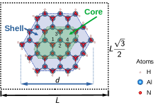
Then, we proceed to the core-shell InAlN NRs. We take as diameter Å, as illustrated in Fig. 1. Even though much larger cells may be required to study realistic NRs,Filho et al. (2023) our goal here is to evaluate the accuracy of LDA-1/2 and mBJ in approximating for these systems. Keeping the computational cost of in mind, we selected these NRs with a relatively small diameter as prototypes for our benchmark. We rationalize that with these NRs, one is still able to draw meaningful conclusions. Then further studies can then profit from our analysis and employ LDA-1/2 or mBJ to investigate NRs with more realistic sizes.
To avoid dangling bonds which lead to spurious states at the Fermi energy, we use H passivation, and, so, the chemical formula of the NR becomes InnAl38-nN38H40. We study three different In concentrations: , 2, and 4. In all cases, we consider an unrelaxed geometry with bond lengths determined from the AlN experimental lattice parameters.Vurgaftman and Meyer (2003) In Fig. 1, we also show a possible split between core and shell regions, leading to the compositions InnAl16-nN16 for the core, and Al22N22H40 for the shell. According to this choice, the cases and 4 correspond to In compositions of 12.5 and 25 % in the core. To isolate neighboring NRs, we employ a supercell with dimensions 44 Bohr 31.1 Bohr ( Å 20.2 Å).
For , we employ a k-grid of to obtain the reference density with LDA, and then to generate the reference KS wavefunctions and eigenvalues. To enable a fair comparison, the same procedure is adopted for LDA, LDA-1/2 and mBJ. For the DOS and the optical properties, we take for all methods 300, 320, and 400 KS states into account, which is sufficient to cover transitions in the energy range eV. In the calculations, we include 900, 920, 940 bands in the summation used to build the dielectric function, with a cutoff of 20 Ry. To speed up the convergence with respect to the vacuum size, we employ a Coulomb truncation for nanowires.Ismail-Beigi (2006)
IV Results
IV.1 Binaries: AlN and InN
The purely binary compositions, AlN and InN, can be seen as benchmarks in relation to the ternary InAlN compounds and their properties are of relevance to the present first-principles comparative study of the InAlN core-shell NRs study.
IV.1.1 DOS and band gaps
In Table 1, the calculated band gaps of AlN and InN are compared with the experimental ones. As usual, LDA band gaps are underestimated for both AlN and InN. With LDA-1/2, although the band gap of InN is overestimated by 0.60 eV, the band gap of AlN agrees with the experimental with an error of 0.04 eV. With mBJ, in contrast, the band gap of InN deviates from experiment by 0.22 eV, while this error is 0.55 eV for AlN. Band gaps obtained with agree with experiment with an error of 0.04 eV for AlN, and of 0.50 eV for InN. Overall, there is a similar degree of agreement with experiment for LDA-1/2, mBJ and .
| AlN | InN | |
|---|---|---|
| 6.29 | 0.28 | |
| LDA | 4.24 | |
| LDA-1/2 | 6.21 | 1.38 |
| mBJ | 5.70 | 0.56 |
| exp. | 6.25 | 0.78 |
Figure 2 depicts the DOS of AlN and InN.
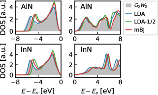
For an easier comparison of the approaches, we plot the DOS of valence and conduction bands separately, on the left and on the right, respectively, placing in each case the band edges at zero. It is apparent then that LDA and have the best agreement, confirming for AlN and InN the common belief that approximately shifts states rigidly. DOS obtained with LDA-1/2 and mBJ agree well with each other and are also very close to .
IV.1.2 Dielectric function
We present the component of dielectric function in Fig. 3.
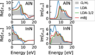
For AlN, the dielectric functions computed with LDA, LDA-1/2 and mBJ are red-shifted when compared to , with LDA showing the largest deviation, and LDA-1/2 presenting a slightly better agreement than mBJ. For InN, the negative gap obtained with LDA causes a qualitative wrong behavior of for small frequencies. LDA-1/2 and mBJ show similar results, with LDA-1/2 closer to .
IV.2 Core-shell InAlN NRs
IV.2.1 DOS
Fig. 4 displays the DOS of core-shell InAlN NRs passivated with hydrogen.
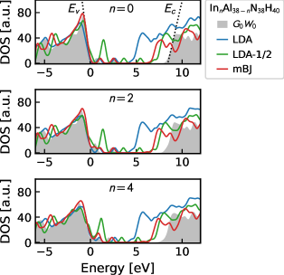
In each case, the zero energy has been defined as follows:
-
1.
projecting the DOS onto core atoms;
-
2.
identifying the valence state with the highest energy ;
-
3.
taking as reference and referring all other energies with respect to it.
The identification of is illustrated for DOS in the top panel of Fig. 4 with the dashed line on the left. Similarly, we can define by projecting the DOS onto core atoms, and taking it as the energy of the conduction band edge. This is shown for as the dashed line on the right in Fig. 4 (subplot on the top).
The isolated peaks observed for energies between 0-5 eV come from states belonging to shell atoms. The agreement between LDA, LDA-1/2, and mBJ with for valence states with is evident for the 3 NRs. For the conduction states with , LDA-1/2 and mBJ match better than LDA. It is also apparent that, the peaks in the energy range 0-5 eV are more pronounced in LDA-1/2 than in other methods.
The definition of and allows us to compute as
| (15) |
can be identified as a kind of band gap for the core region of the NR, since it is obtained from band edges of states that belong to core atoms.
Table 2 presents for each NR. The best agreement with is given by LDA-1/2, with approximately 1.2 eV smaller.
| 0 | 2 | 4 | |
|---|---|---|---|
| 8.44 | 8.38 | 8.14 | |
| LDA | 4.69 | 4.76 | 4.75 |
| LDA-1/2 | 7.26 | 7.19 | 7.00 |
| mBJ | 6.66 | 6.71 | 6.55 |
mBJ comes next, predicting 1.6-1.8 eV smaller than . LDA is the last one with 3.4-3.7 eV smaller than .
When compared to bulk AlN, the NRs are expected to have larger due to quantum confinement effects. Indeed, the passivated AlN NR has larger than bulk AlN by 2.15, 0.45, 1.05 and 0.96 and eV, when calculated with , LDA, LDA-1/2 and mBJ respectively. As estimated in Appendix B, an enlargement of 1.9-2.5 eV is expected due to quantum confinement effects. best matches this expectation, followed by LDA-1/2, mBJ and LDA.
IV.2.2 Optical properties
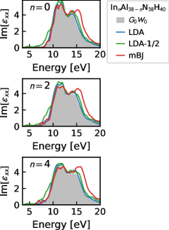
Figure 5 displays the component of the dielectric function.
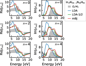
LDA-1/2 and mBJ agree well with each other and are red-shifted by 1.8 and 2.0 eV, respectively, in comparison with . For LDA, this amounts to 3.5 eV. By blue-shifting all Im, a good agreement with can be observed, as shown in Appendix C. Although these shifts do not reproduce exactly the differences in , they are comparable.
Next, we consider the contribution of In atoms present in the core region to the dielectric function of the NRs. In Fig. 5, it is evident that the presence of In introduces peaks in , which are red-shifted in respect to the main peak observed for AlN NRs without In. These peaks, highlighted with arrows in Fig. 5, become evident when we for NRs with In and by for AlN NRs (not shown here). Table 3 shows the positions of these peaks due to In.
| 2 | 4 | |
|---|---|---|
| 7.70 | 6.96 | |
| LDA | 4.64 | 4.28 |
| LDA-1/2 | 6.37 | 5.77 |
| mBJ | 5.69 | 4.97 |
Peaks within appear blue-shifted in comparison with other methods. Peaks obtained with LDA-1/2 exhibit best agreement with , with a difference of 1.2-1.3 eV. These numbers are 2.0 and 3.1-3.4 eV for mBJ and LDA, respectively. Also interesting is that the red-shift of the peaks observed by increasing to is approximately the same in (0.74 eV), LDA-1/2 (0.60 eV) and mBJ (0.72 eV).
In Fig. 6, we depict the refraction index and the extinction coefficient for the energy range of 0 to 20 eV.
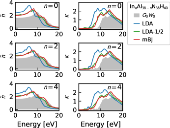
The similarity between LDA-1/2 and mBJ is apparent. Regarding the refraction index, for the energy range 10-20 eV, LDA-1/2 and mBJ show an excellent agreement with . Although this statement does not hold for the extinction coefficient, there is a notable improvement over LDA: LDA-1/2 and mBJ approximate better than LDA.
Table 4 presents the static refractive index. The best agreement with respect to is observed for mBJ (difference of 12-13%), closely followed by LDA-1/2 (14%) and, then, by LDA (26-27%).
| 0 | 2 | 4 | |
|---|---|---|---|
| 1.59 | 1.61 | 1.63 | |
| LDA | 2.38 | 2.40 | 2.43 |
| LDA-1/2 | 2.03 | 2.05 | 2.07 |
| mBJ | 1.97 | 1.99 | 2.02 |
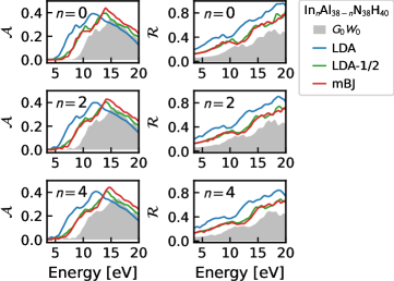
Figure 7 depicts the absorbance and the reflectance of the NRs. The curves for LDA-1/2 and mBJ are very similar, and both present a better agreement with than LDA.
V Conclusion
We have studied electronic and optical properties of core-shell InAlN NRs with LDA, LDA-1/2, mBJ and . For the properties, DOS, dielectric function, refractive index, extinction coefficient, absorption coefficient, and reflectance: results with LDA-1/2 and mBJ are similar and agree better with than those obtained with LDA. For band gaps and peaks in Im coming from In contributions, LDA-1/2 agrees better with than mBJ. Overall, LDA-1/2 and mBJ can be used as tools to replace with reasonable accuracy at much less computational cost.
The authors have no conflicts to disclose. The data that support the findings of this study are available from the corresponding author upon reasonable request.
Acknowledgements.
The authors gratefully acknowledge the computing time granted by the Resource Allocation Board and provided on the supercomputer Lise and Emmy at NHR@ZIB and NHR@Göttingen as part of the NHR infrastructure. They also acknowledge resources provided by the National Academic Infrastructure for Supercomputing in Sweden (NAISS) at the National Supercomputer Center (NSC) in Linköping (NAISS 2023/5-116 and NAISS 2023/23-161) partially funded by the Swedish Research Council through grant agreement no. 2018-05973. G. K. G., J. B., and L. H. acknowledge support by the Swedish Government Strategic Research Area in Materials Science on Advanced Functional Materials (AFM) at Linköping University (Faculty Grant SFO-Mat-LiU No. 2009-00971). C.-L.H. acknowledges support by the Swedish Research Council (Vetenskapsrådet) through grant number 2018-04198 and the Swedish Energy Agency (Energimyndigheten) through grant number 46658-1.References
- Taniyasu, Kasu, and Makimoto (2006) Y. Taniyasu, M. Kasu, and T. Makimoto, “An aluminium nitride light-emitting diode with a wavelength of 210 nanometres,” nature 441, 325–328 (2006).
- Wu et al. (2002) J. Wu, W. Walukiewicz, K. Yu, J. Ager Iii, E. Haller, H. Lu, W. J. Schaff, Y. Saito, and Y. Nanishi, “Unusual properties of the fundamental band gap of inn,” Applied Physics Letters 80, 3967–3969 (2002).
- Hsiao et al. (2007) C.-L. Hsiao, H.-C. Hsu, L.-C. Chen, C.-T. Wu, C.-W. Chen, M. Chen, L.-W. Tu, and K.-H. Chen, “Photoluminescence spectroscopy of nearly defect-free inn microcrystals exhibiting nondegenerate semiconductor behaviors,” Applied Physics Letters 91, 181912 (2007).
- Baten et al. (2021) M. Z. Baten, S. Alam, B. Sikder, and A. Aziz, “III-Nitride light-emitting devices,” Photonics 8 (2021), 10.3390/photonics8100430.
- Alias et al. (2018) M. S. Alias, M. Tangi, J. A. Holguin-Lerma, E. Stegenburgs, A. A. Alatawi, I. Ashry, R. C. Subedi, D. Priante, M. K. Shakfa, T. K. Ng, et al., “Review of nanophotonics approaches using nanostructures and nanofabrication for iii-nitrides ultraviolet-photonic devices,” Journal of Nanophotonics 12, 043508–043508 (2018).
- Huang et al. (2019) X. Huang, W. Li, H. Fu, D. Li, C. Zhang, H. Chen, Y. Fang, K. Fu, S. P. DenBaars, S. Nakamura, et al., “High-temperature polarization-free iii-nitride solar cells with self-cooling effects,” ACS Photonics 6, 2096–2103 (2019).
- Li et al. (2017) L. Li, D. Hosomi, Y. Miyachi, T. Hamada, M. Miyoshi, and T. Egawa, “High-performance ultraviolet photodetectors based on lattice-matched inaln/algan heterostructure field-effect transistors gated by transparent ito films,” Applied Physics Letters 111, 102106 (2017).
- Filho et al. (2023) M. A. M. Filho, C.-L. Hsiao, R. B. d. Santos, L. Hultman, J. Birch, and G. K. Gueorguiev, “Self-Induced Core–Shell InAlN Nanorods: Formation and Stability Unraveled by Ab Initio Simulations,” ACS Nanoscience Au 3, 84–93 (2023).
- Nanishi, Saito, and Yamaguchi (2003) Y. Nanishi, Y. Saito, and T. Yamaguchi, “Rf-molecular beam epitaxy growth and properties of inn and related alloys,” Japanese journal of applied physics 42, 2549 (2003).
- Ferhat and Bechstedt (2002) M. Ferhat and F. Bechstedt, “First-principles calculations of gap bowing in and alloys: Relation to structural and thermodynamic properties,” Phys. Rev. B 65, 075213 (2002).
- Palisaitis et al. (2017) J. Palisaitis, C.-L. Hsiao, L. Hultman, J. Birch, and P. Persson, “Direct observation of spinodal decomposition phenomena in inaln alloys during in-situ stem heating,” Scientific reports 7, 1–8 (2017).
- Goyenola et al. (2012) C. Goyenola, S. Stafstrom, L. Hultman, Gueorguiev, and G. K, “Structural patterns arising during synthetic growth of fullerene-like sulfocarbide,” The Journal of Physical Chemistry C 116, 21124–21131 (2012).
- Gueorguiev et al. (2011) G. K. Gueorguiev, Z. Czigány, A. Furlan, S. Stafström, and L. Hultman, “Intercalation of p atoms in fullerene-like cpx,” Chemical Physics Letters 501, 400–403 (2011).
- Gueorguiev et al. (2006) G. K. Gueorguiev, A. Furlan, H. Högberg, S. Stafström, and L. Hultman, “First-principles calculations on the structural evolution of solid fullerene-like cpx,” Chemical physics letters 426, 374–379 (2006).
- Goyenola et al. (2011) C. Goyenola, G. K. Gueorguiev, S. Stafström, and L. Hultman, “Fullerene-like csx: A first-principles study of synthetic growth,” Chemical Physics Letters 506, 86–91 (2011).
- Kamimura et al. (2007) J. Kamimura, T. Kouno, S. Ishizawa, A. Kikuchi, and K. Kishino, “Growth of high-In-content InAlN nanocolumns on Si (1 1 1) by RF-plasma-assisted molecular-beam epitaxy,” Journal of crystal growth 300, 160–163 (2007).
- Prabaswara et al. (2020) A. Prabaswara, J. Birch, M. Junaid, E. A. Serban, L. Hultman, and C.-L. Hsiao, “Review of gan thin film and nanorod growth using magnetron sputter epitaxy,” Applied Sciences 10, 3050 (2020).
- Serban et al. (2017) E. A. Serban, J. Palisaitis, M. Junaid, L. Tengdelius, H. Högberg, L. Hultman, P. O. Å. Persson, J. Birch, and C.-L. Hsiao, “Magnetron sputter epitaxy of high-quality gan nanorods on functional and cost-effective templates/substrates,” Energies 10, 1322 (2017).
- Hsiao et al. (2015) C.-L. Hsiao, R. Magnusson, J. Palisaitis, P. Sandström, P. O. Persson, S. Valyukh, L. Hultman, K. Järrendahl, and J. Birch, “Curved-lattice epitaxial growth of Inx Al1–x N Nanospirals with tailored chirality,” Nano Letters 15, 294–300 (2015).
- Kuo et al. (2018) Y.-H. Kuo, R. Magnusson, E. A. Serban, P. Sandström, L. Hultman, K. Järrendahl, J. Birch, and C.-L. Hsiao, “Influence of InAlN nanospiral structures on the behavior of reflected light polarization,” Nanomaterials 8, 157 (2018).
- Yao et al. (2017) C. Yao, X. Ye, R. Sun, G. Yang, J. Wang, Y. Lu, P. Yan, and J. Cao, “AlGaN solar-blind avalanche photodiodes with AlInN/AlGaN distributed bragg reflectors,” Applied Physics A 123, 1–4 (2017).
- Ristić et al. (2005) J. Ristić, E. Calleja, A. Trampert, S. Fernández-Garrido, C. Rivera, U. Jahn, and K. H. Ploog, “Columnar nanocavities with bragg reflectors grown by molecular beam epitaxy on si(111),” Phys. Rev. Lett. 94, 146102 (2005).
- Takeuchi et al. (2018) T. Takeuchi, S. Kamiyama, M. Iwaya, and I. Akasaki, “GaN-based vertical-cavity surface-emitting lasers with AlInN/GaN distributed Bragg reflectors,” Reports on Progress in Physics 82, 012502 (2018).
- Aryasetiawan and Gunnarsson (1998) F. Aryasetiawan and O. Gunnarsson, “The GW method,” Reports on Progress in Physics 61, 237 (1998).
- Onida, Reining, and Rubio (2002) G. Onida, L. Reining, and A. Rubio, “Electronic excitations: density-functional versus many-body Green’s-function approaches,” Reviews of Modern Physics 74, 601–659 (2002).
- Bechstedt (2015) F. Bechstedt, Many-Body Approach to Electronic Excitations, 1st ed. (Springer Berlin, Heidelberg, 2015).
- Golze, Dvorak, and Rinke (2019) D. Golze, M. Dvorak, and P. Rinke, “The GW Compendium: A Practical Guide to Theoretical Photoemission Spectroscopy,” Frontiers in Chemistry 7, 377 (2019).
- Reining (2018) L. Reining, “The GW approximation: content, successes and limitations,” Wiley Interdisciplinary Reviews: Computational Molecular Science 8 (2018), 10.1002/wcms.1344.
- Nabok, Gulans, and Draxl (2016) D. Nabok, A. Gulans, and C. Draxl, “Accurate all-electron $G_0W_0$ quasiparticle energies employing the full-potential augmented planewave method,” Physical Review B 94, 035118 (2016), 1605.07351 .
- Govoni and Galli (2015) M. Govoni and G. Galli, “Large scale GW calculations,” Journal of Chemical Theory and Computation 11, 2680–2696 (2015).
- van Setten et al. (2015) M. J. van Setten, F. Caruso, S. Sharifzadeh, X. Ren, M. Scheffler, F. Liu, J. Lischner, L. Lin, J. R. Deslippe, S. G. Louie, C. Yang, F. Weigend, J. B. Neaton, F. Evers, and P. Rinke, “GW100: Benchmarking G0W0 for Molecular Systems,” Journal of Chemical Theory and Computation 11, 5665–5687 (2015).
- Krause, Harding, and Klopper (2015) K. Krause, M. E. Harding, and W. Klopper, “Coupled-cluster reference values for the GW27 and GW100 test sets for the assessment of GW methods,” Molecular Physics 113, 1952–1960 (2015).
- Pela, Marques, and Teles (2015) R. R. Pela, M. Marques, and L. K. Teles, “Comparing LDA-1/2, HSE03, HSE06 and G 0 W 0 approaches for band gap calculations of alloys,” Journal of Physics: Condensed Matter 27, 505502 (2015).
- Ferreira, Marques, and Teles (2008) L. G. Ferreira, M. Marques, and L. K. Teles, “Approximation to density functional theory for the calculation of band gaps of semiconductors,” Phys. Rev. B 78, 125116 (2008).
- Ferreira, Marques, and Teles (2011) L. G. Ferreira, M. Marques, and L. K. Teles, “Slater half-occupation technique revisited: the LDA-1/2 and GGA-1/2 approaches for atomic ionization energies and band gaps in semiconductors,” AIP Advances 1, 032119 (2011).
- Pelá et al. (2012) R. R. Pelá, M. Marques, L. G. Ferreira, J. Furthmüller, and L. K. Teles, “GaMnAs: Position of Mn- d levels and majority spin band gap predicted from GGA-1/2 calculations,” Applied Physics Letters 100, 202408 (2012).
- Pela et al. (2016) R. R. Pela, U. Werner, D. Nabok, and C. Draxl, “Probing the LDA-1/2 method as a starting point for G0W0 calculations,” Physical Review B 94, 235141 (2016).
- Pela, Gulans, and Draxl (2018) R. R. Pela, A. Gulans, and C. Draxl, “The LDA-1/2 method applied to atoms and molecules,” Journal of Chemical Theory and Computation (2018), 10.1021/acs.jctc.8b00518, 1805.09705 .
- Matusalem et al. (2013) F. Matusalem, M. Ribeiro, Jr., M. Marques, R. R. Pelá, L. G. Ferreira, and L. K. Teles, “Combined lda and lda-1/2 method to obtain defect formation energies in large silicon supercells,” Phys. Rev. B 88, 224102 (2013).
- Pelá et al. (2011) R. R. Pelá, C. Caetano, M. Marques, L. G. Ferreira, J. Furthmüller, and L. K. Teles, “Accurate band gaps of AlGaN, InGaN, and AlInN alloys calculations based on LDA-1/2 approach,” Applied Physics Letters 98, 151907 (2011).
- Filho et al. (2013) O. P. S. Filho, M. Ribeiro, R. R. Pelá, L. K. Teles, L. G. Ferreira, and M. Marques, “All-out band structure and band offset ab initio predictions for AlN/GaN and AlP/GaP interfaces,” Journal of Applied Physics 114, 033709 (2013).
- Santos et al. (2012) J. P. T. Santos, M. Marques, L. G. Ferreira, R. R. Pelá, and L. K. Teles, “Digital magnetic heterostructures based on GaN using GGA-1/2 approach,” Applied Physics Letters 101, 112403 (2012).
- Matusalem et al. (2020) F. Matusalem, M. Marques, I. Guilhon, and L. K. Teles, “Efficient calculation of excitonic effects in solids including approximated quasiparticle energies,” Journal of Physics: Condensed Matter 32, 405505 (2020), 2003.11968 .
- Ribeiro (2015) M. Ribeiro, “Ab initio quasi-particle approximation bandgaps of silicon nanowires calculated at density functional theory/local density approximation computational effort,” Journal of Applied Physics 117, 234302 (2015).
- Huang et al. (2015) P. Huang, H. Zong, J.-j. Shi, M. Zhang, X.-h. Jiang, H.-x. Zhong, Y.-m. Ding, Y.-p. He, J. Lu, and X.-d. Hu, “Origin of 3.45 eV Emission Line and Yellow Luminescence Band in GaN Nanowires: Surface Microwire and Defect,” ACS Nano 9, 9276–9283 (2015).
- Greil et al. (2016) J. Greil, S. Assali, Y. Isono, A. Belabbes, F. Bechstedt, F. O. V. Mackenzie, A. Y. Silov, E. P. A. M. Bakkers, and J. E. M. Haverkort, “Optical Properties of Strained Wurtzite Gallium Phosphide Nanowires,” Nano Letters 16, 3703–3709 (2016).
- Tran et al. (2019) F. Tran, J. Doumont, L. Kalantari, A. W. Huran, M. A. L. Marques, and P. Blaha, “Semilocal exchange-correlation potentials for solid-state calculations: Current status and future directions,” Journal of Applied Physics 126, 110902 (2019), 1908.01820 .
- Tran and Blaha (2009) F. Tran and P. Blaha, “Accurate Band Gaps of Semiconductors and Insulators with a Semilocal Exchange-Correlation Potential,” Physical Review Letters 102, 226401 (2009).
- Koller, Tran, and Blaha (2011) D. Koller, F. Tran, and P. Blaha, “Merits and limits of the modified Becke-Johnson exchange potential,” Physical Review B 83 (2011), 10.1103/physrevb.83.195134.
- Kim et al. (2010) Y.-S. Kim, M. Marsman, G. Kresse, F. Tran, and P. Blaha, “Towards efficient band structure and effective mass calculations for iii-v direct band-gap semiconductors,” Phys. Rev. B 82, 205212 (2010).
- Jiang (2013) H. Jiang, “Band gaps from the tran-blaha modified becke-johnson approach: A systematic investigation,” The Journal of Chemical Physics 138, 134115 (2013).
- Lee et al. (2016) J. Lee, A. Seko, K. Shitara, K. Nakayama, and I. Tanaka, “Prediction model of band gap for inorganic compounds by combination of density functional theory calculations and machine learning techniques,” Phys. Rev. B 93, 115104 (2016).
- Wang et al. (2013) Y. Wang, H. Yin, R. Cao, F. Zahid, Y. Zhu, L. Liu, J. Wang, and H. Guo, “Electronic structure of iii-v zinc-blende semiconductors from first principles,” Phys. Rev. B 87, 235203 (2013).
- Li and Singh (2017) Y. Li and D. J. Singh, “Properties of the ferroelectric visible light absorbing semiconductors: Sn2P2S6 and Sn2P2Se6,” Physical Review Materials 1, 075402 (2017), 1711.08022 .
- Ibarra-Hernández et al. (2017) W. Ibarra-Hernández, H. Elsayed, A. H. Romero, A. Bautista-Hernández, D. Olguín, and A. Cantarero, “Electronic structure, lattice dynamics, and optical properties of a novel van der waals semiconductor heterostructure: ,” Phys. Rev. B 96, 035201 (2017).
- Rödl et al. (2019) C. Rödl, J. Furthmüller, J. R. Suckert, V. Armuzza, F. Bechstedt, and S. Botti, “Accurate electronic and optical properties of hexagonal germanium for optoelectronic applications,” Phys. Rev. Mater. 3, 034602 (2019).
- Singh (2010) D. J. Singh, “Structure and optical properties of high light output halide scintillators,” Phys. Rev. B 82, 155145 (2010).
- Ondračka et al. (2017) P. Ondračka, D. Holec, D. Nečas, E. Kedroňová, S. Elisabeth, A. Goullet, and L. Zajíčková, “Optical properties of solid solutions,” Phys. Rev. B 95, 195163 (2017).
- Nakano and Sakai (2018) K. Nakano and T. Sakai, “Assessing the performance of the Tran–Blaha modified Becke–Johnson exchange potential for optical constants of semiconductors in the ultraviolet–visible light region,” Journal of Applied Physics 123, 015104 (2018).
- Rehman et al. (2016) G. Rehman, M. Shafiq, Saifullah, R. Ahmad, S. Jalali-Asadabadi, M. Maqbool, I. Khan, H. Rahnamaye-Aliabad, and I. Ahmad, “Electronic Band Structures of the Highly Desirable III–V Semiconductors: TB-mBJ DFT Studies,” Journal of Electronic Materials 45, 3314–3323 (2016).
- Radzwan et al. (2019) A. Radzwan, R. Ahmed, A. Shaari, and A. Lawal, “Ab initio calculations of antimony sulphide nanowire,” Physica B: Condensed Matter 557, 17–22 (2019).
- Xiang and Yang (2017) L. Xiang and S. Yang, “Uniaxial strain-modulated electronic structures of cdx (x = s, se, te) from first-principles calculations: A comparison between bulk and nanowires*,” Chinese Physics B 26, 087103 (2017).
- Park et al. (2022) K. Park, D. Kim, T. T. Debela, M. Boujnah, G. M. Zewdie, J. Seo, I. S. Kwon, I. H. Kwak, M. Jung, J. Park, et al., “Polymorphic ga2s3 nanowires: phase-controlled growth and crystal structure calculations,” Nanoscale Advances 4, 3218–3225 (2022).
- Validžić et al. (2014) I. L. Validžić, M. Mitrić, N. Abazović, B. M. Jokić, A. S. Milošević, Z. S. Popović, and F. R. Vukajlović, “Structural analysis, electronic and optical properties of the synthesized sb2s3 nanowires with small band gap,” Semiconductor Science and Technology 29, 035007 (2014).
- Gueorguiev, Stafström, and Hultman (2008) G. K. Gueorguiev, S. Stafström, and L. Hultman, “Nano-wire formation by self-assembly of silicon–metal cage-like molecules,” Chemical Physics Letters 458, 170–174 (2008).
- de Oliveira et al. (2021) M. I. A. de Oliveira, R. Rivelino, F. de Brito Mota, A. Kakanakova-Georgieva, and G. K. Gueorguiev, “Optical properties of organosilicon compounds containing sigma-electron delocalization by quasiparticle self-consistent gw calculations,” Spectrochimica Acta Part A: Molecular and Biomolecular Spectroscopy 245, 118939 (2021).
- Mao et al. (2022) G.-Q. Mao, Z.-Y. Yan, K.-H. Xue, Z. Ai, S. Yang, H. Cui, J.-H. Yuan, T.-L. Ren, and X. Miao, “DFT-1/2 and shell DFT-1/2 methods: electronic structure calculation for semiconductors at LDA complexity,” Journal of Physics: Condensed Matter 34, 403001 (2022).
- Kohn and Sham (1965) W. Kohn and L. J. Sham, “Self-consistent equations including exchange and correlation effects,” Phys. Rev. 140, A1133–A1138 (1965).
- Becke and Roussel (1989) A. D. Becke and M. R. Roussel, “k.p method for strained wurtzite semiconductors,” Physical Review A 39, 3761–3767 (1989).
- Rangel et al. (2020) T. Rangel, M. D. Ben, D. Varsano, G. Antonius, F. Bruneval, F. H. d. Jornada, M. J. v. Setten, O. K. Orhan, D. D. O’Regan, A. Canning, A. Ferretti, A. Marini, G.-M. Rignanese, J. Deslippe, S. G. Louie, and J. B. Neaton, “Reproducibility in G 0 W 0 calculations for solids,” Computer Physics Communications 255, 107242 (2020), 1903.06865 .
- Freysoldt et al. (2007) C. Freysoldt, P. Eggert, P. Rinke, A. Schindlmayr, R. Godby, and M. Scheffler, “Dielectric anisotropy in the GW space–time method,” Computer Physics Communications 176, 1–13 (2007), cond-mat/0608215 .
- Bassani and Pastori Parravicini (1975) F. Bassani and G. Pastori Parravicini, Electronic states and optical transitions in solids, 1st ed. (Pergamon Press, 1975).
- Yu and Cardona (2010) P. Y. Yu and M. Cardona, Fundamentals of Semiconductors, 1st ed. (Springer Berlin, Heidelberg, 2010).
- Dresselhaus et al. (2018) M. Dresselhaus, G. Dresselhaus, S. Cronin, and A. G. S. Filho, Solid State Properties, From Bulk to Nano, 1st ed. (Springer Berlin, Heidelberg, 2018).
- Giannozzi et al. (2009) P. Giannozzi, S. Baroni, N. Bonini, M. Calandra, R. Car, C. Cavazzoni, D. Ceresoli, G. L. Chiarotti, M. Cococcioni, I. Dabo, A. D. Corso, S. de Gironcoli, S. Fabris, G. Fratesi, R. Gebauer, U. Gerstmann, C. Gougoussis, A. Kokalj, M. Lazzeri, L. Martin-Samos, N. Marzari, F. Mauri, R. Mazzarello, S. Paolini, A. Pasquarello, L. Paulatto, C. Sbraccia, S. Scandolo, G. Sclauzero, A. P. Seitsonen, A. Smogunov, P. Umari, and R. M. Wentzcovitch, “Quantum espresso: a modular and open-source software project for quantum simulations of materials,” Journal of Physics: Condensed Matter 21, 395502 (2009).
- Giannozzi et al. (2017) P. Giannozzi, O. Andreussi, T. Brumme, O. Bunau, M. B. Nardelli, M. Calandra, R. Car, C. Cavazzoni, D. Ceresoli, M. Cococcioni, N. Colonna, I. Carnimeo, A. D. Corso, S. de Gironcoli, P. Delugas, R. A. DiStasio, A. Ferretti, A. Floris, G. Fratesi, G. Fugallo, R. Gebauer, U. Gerstmann, F. Giustino, T. Gorni, J. Jia, M. Kawamura, H.-Y. Ko, A. Kokalj, E. Küçükbenli, M. Lazzeri, M. Marsili, N. Marzari, F. Mauri, N. L. Nguyen, H.-V. Nguyen, A. O. de-la Roza, L. Paulatto, S. Poncé, D. Rocca, R. Sabatini, B. Santra, M. Schlipf, A. P. Seitsonen, A. Smogunov, I. Timrov, T. Thonhauser, P. Umari, N. Vast, X. Wu, and S. Baroni, “Advanced capabilities for materials modelling with quantum espresso,” Journal of Physics: Condensed Matter 29, 465901 (2017).
- Giannozzi et al. (2020) P. Giannozzi, O. Baseggio, P. Bonf‘a, D. Brunato, R. Car, I. Carnimeo, C. Cavazzoni, S. de Gironcoli, P. Delugas, F. Ferrari Ruffino, A. Ferretti, N. Marzari, I. Timrov, A. Urru, and S. Baroni, “Quantum espresso toward the exascale,” The Journal of Chemical Physics 152, 154105 (2020).
- Hamann (2013) D. R. Hamann, “Optimized norm-conserving vanderbilt pseudopotentials,” Phys. Rev. B 88, 085117 (2013).
- Deslippe et al. (2012) J. Deslippe, G. Samsonidze, D. A. Strubbe, M. Jain, M. L. Cohen, and S. G. Louie, “BerkeleyGW: A massively parallel computer package for the calculation of the quasiparticle and optical properties of materials and nanostructures,” Computer Physics Communications 183, 1269–1289 (2012), 1111.4429 .
- Hybertsen and Louie (1986) M. S. Hybertsen and S. G. Louie, “Electron correlation in semiconductors and insulators: Band gaps and quasiparticle energies,” Phys. Rev. B 34, 5390–5413 (1986).
- Deslippe et al. (2013) J. Deslippe, G. Samsonidze, M. Jain, M. L. Cohen, and S. G. Louie, “Coulomb-hole summations and energies for calculations with limited number of empty orbitals: A modified static remainder approach,” Phys. Rev. B 87, 165124 (2013).
- Zhang et al. (1989) S. B. Zhang, D. Tománek, M. L. Cohen, S. G. Louie, and M. S. Hybertsen, “Evaluation of quasiparticle energies for semiconductors without inversion symmetry,” Phys. Rev. B 40, 3162–3168 (1989).
- Vurgaftman and Meyer (2003) I. Vurgaftman and J. R. Meyer, “Band parameters for nitrogen-containing semiconductors,” Journal of Applied Physics 94, 3675–3696 (2003).
- Ismail-Beigi (2006) S. Ismail-Beigi, “Truncation of periodic image interactions for confined systems,” Physical Review B 73, 233103 (2006), cond-mat/0603448 .
- Klimeš, Kaltak, and Kresse (2014) J. Klimeš, M. Kaltak, and G. Kresse, “Predictive GW calculations using plane waves and pseudopotentials,” Physical Review B 90, 075125 (2014).
- Robinett (1996) R. W. Robinett, “Visualizing the solutions for the circular infinite well in quantum and classical mechanics,” American Journal of Physics 64, 440–446 (1996).
- Chuang and Chang (1996) S. L. Chuang and C. S. Chang, “k.p method for strained wurtzite semiconductors,” Physical Review B 54, 2491–2504 (1996).
Appendixes
Appendix A Convergence behavior
A.1 Bulk AlN and InN
Figures 8 and 9 show, for bulk AlN and InN, the convergence behavior of the band gap. Two parameters are varied: the number of KS states () and the planewave cutoff () used to build the dielectric function.
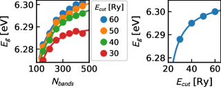
The convergence of band gap is slower than that of DFT. Having a fully converged band gap is challenging, as employing a set of fully converged parameters comes with a very high computational cost. Therefore, we follow here an extrapolation procedure to evaluate the band gap, adopting the expressionKlimeš, Kaltak, and Kresse (2014); Nabok, Gulans, and Draxl (2016); Pela et al. (2016):
| (16) |
where , and are fit coefficients, and is the convergence parameter being tested, which can be or . Assuming that the extrapolation with respect to , and the k-grid can be carried out separately, the extrapolated band gap can be evaluated as
| (17) |
where is the band gap for a reference calculation employing , , and . We adopt for AlN: , Ry; and for InN: , Ry; and, in both cases, as .
Then and are obtained as
| (18) |
| (19) |
and the contribution of the k-grid to the extrapolation is approximated asKlimeš, Kaltak, and Kresse (2014); Nabok, Gulans, and Draxl (2016); Pela et al. (2016):
| (20) |
where is employed as .
Table 5 collects the relevant data regarding the extrapolation of the band gap.
| AlN | 6.28 | 0.03 | 0.01 | -0.03 | 6.29 |
| InN | 0.09 | 0.02 | 0.03 | 0.14 | 0.28 |
A.2 Nanorods
A.2.1 Vacuum
In Eq. (10), stands for the volume of the sample. However, in most of ab initio codes, including Quantum Espresso, is treated as the unit cell volume. For systems with vacuum in the unit cell, such as the NRs studied here, the dielectric function must be corrected by a factor equal to the ratio between the volumes of the cell and the sample. In terms of the geometry shown in Fig. 1, we have for the NRs
| (21) |
where and are the cross-sections of the unit cell and the NR, respectively.
Denoting as the dielectric function without the correction and , the corrected one, then according to Eqs. (10) and (12), it follows that:
| (22) |
| (23) |
Figure 10 depicts the convergence behavior of the dielectric function with respect to cell dimension .
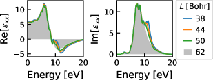
These calculations refer to the AlN NR and have been carried out with LDA, and a similar trend has been observed for the other cases. Fig. 10 shows that the size Bohr, adopted for the NRs calculations reported in the present work, is sufficient to guarantee satisfactory convergence within the energy range of eV.
A.2.2 Band gap
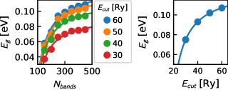
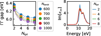
Here, we discuss the precision level expected for our calculations concerning the NRs. As for bulk AlN and InN, we check convergence with respect to , and the k-grid . For the sake of computational cost, we restrict the analysis to the band gap and the dielectric function of AlN.
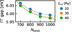
Figure 11 depicts on the left side the impact of and on the band gap. Since we adopted and , we estimate, by making the extrapolation procedure as described in Appendix A.1, a correction of eV and eV.
On the right side of Fig. 11, we present the imaginary part of dielectric function. Even though the band gap has a more pronounced dependence on , the dielectric function exhibits good convergence already for .
Figure 12 displays the influence of and on the band gap. Following the extrapolation procedure, we evaluate a correction of eV for the adopted Ry. Overall, by adding up , and , we expect that band gaps are overestimated by about 0.2 eV.
Appendix B Quantum confinement and band gap
The expected band gap enlargement due to quantum confinement effects can be estimated by considering a particle of mass confined inside a circular quantum well of radius . Following Ref. Robinett, 1996, we have, in atomic units:
| (24) |
where is the first zero of , Bessel’s function of order zero. To estimate for the case of the NRs, we approximate by the reduced mass of the electron and the heavy hole, . Taking the suggested values in Ref. Vurgaftman and Meyer, 2003: , in atomic units. is obtained from the Pikus-Bir parameters given in Ref. Vurgaftman and Meyer, 2003 asChuang and Chang (1996)
| (25) |
which gives , in atomic units. Therefore .
Lastly, we consider a range for between the radius of the inscribed and the circumscribed circles in the NRs. Taking into account the NR diameter of Å, this implies that lies between and Å. Applying Eq. (24) gives the range of - eV for .
Appendix C Shift in the dielectric function
Figure 13 shows, for the NRs, of the different DFT approaches blue-shifted by to better match . To plot these curves, we shift the vertical transitions in Eq. (10), so that the shifted dielectric function at a given frequency relates to the original by:
| (26) |
It is observed that, setting to 3.5, 1.8 and 2.0 eV for LDA, LDA-1/2 and mBJ, respectively, leads to an excellent agreement with obtained with .