Real-time feedback protocols for optimizing fault-tolerant two-qubit gate fidelities in a silicon spin system
Abstract
Recently, several groups have demonstrated two-qubit gate fidelities in semiconductor spin qubit systems above 99%. Achieving this regime of fault-tolerant compatible high fidelities is nontrivial and requires exquisite stability and precise control over the different qubit parameters over an extended period of time. This can be done by efficiently calibrating qubit control parameters against different sources of micro- and macroscopic noise. Here, we present several single- and two-qubit parameter feedback protocols, optimised for and implemented in state-of-the-art fast FPGA hardware. Furthermore, we use wavelet-based analysis on the collected feedback data to gain insight into the different sources of noise in the system. Scalable feedback is an outstanding challenge and the presented implementation and analysis gives insight into the benefits and drawbacks of qubit parameter feedback, as feedback related overhead increases. This work demonstrates a pathway towards robust qubit parameter feedback and systematic noise analysis, crucial for mitigation strategies towards systematic high-fidelity qubit operation compatible with quantum error correction protocols.
Recent demonstrations of silicon spin qubit systems with two-qubit gate fidelities above 99% confirm the promise of the qubit platform for large-scale quantum computing [1, 2, 3, 4]. However, fault-tolerant quantum computing will require consistent high-fidelity single- and two-qubit control, both over an extended period of time, and over an extended array of devices [5, 4]. Therefore, precise qubit parameter control and a better understanding of the origin of the noise acting on the qubit system are crucial steps towards developing mitigating strategies, both in device fabrication and operation.
Parameter feedback plays a key role in the stability and performance of qubit devices in the field of quantum computing [6, 7, 4, 8, 9]. A typical feedback protocol measures the status of a system and adjusts the system’s control parameters to counteract any unwanted change. Feedback data, or control parameter correction data, is useful for several purposes. Firstly, it indicates if an experiment ran successfully, as it reflects the stability of different qubit parameters during the run time. Next, feedback can improve key characteristics of the system being studied, such as the quality factor of Rabi oscillations in the case of qubit data [6, 7]. Finally, the feedback data contains valuable information about noise signals impacting the system and their dynamics. Understanding these signals can lead to improvements in qubit control and device fabrication, but efficiently extracting information is still an outstanding challenge [10].
One promising technique for advanced noise analysis is wavelet analysis as it allows to characterise and analyse the complex dynamics of quantum systems [11, 12]. Quantum systems typically display both time dependent and independent signals. Time dependent signals can be stationary with a constant periodicity, or non-stationary, with a periodicity that changes over time. Wavelet analysis can identify non-stationary signals providing insight on the duration, frequency and occurrence time(s) of an event, making it more powerful and better suited for qubit feedback data than a standard Fourier analysis [13, 14, 15].
In this Letter, we present fast feedback protocols for several single- and two-qubit parameters for spin qubits in a silicon quantum dot system. The feedback protocols are optimised for fast FPGA based hardware and are executed in real-time. We then demonstrate how wavelet transformations on the feedback protocol data can help identify different noise characteristics in the qubit system, and give additional insight compared to the well-established Fourier transform.
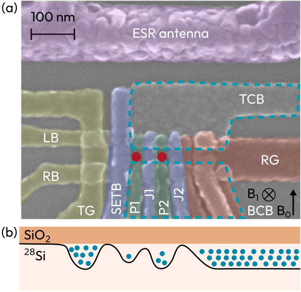
Figure 1(a) shows a scanning electron microscope image of a device nominally identical to the one used in the experiment, accompanied by a schematic cross-section in Figure 1(b). The device accumulates electrons at the interface between the SiO2 dielectric and isotopically enriched 28Si substrate (800 ppm) using gate electrodes fabricated in an Al/AlOx gate stack [7]. We operate the device with a fixed number of electrons in the so-called ‘isolation’ mode [16]. The left and right dots are formed under plunger gates P1 and P2 containing one electron and three electrons, respectively, written as (1,3) [16, 17]. Top and bottom confinement barrier gates, TCB and BCB, respectively, surround the dots laterally. Exchange interaction between the quantum dot sites is activated by applying a voltage to the interstitial J1 gate. An in-plane applied static magnetic field of 0.7 T splits the spin up and down states of the unpaired electrons, forming the two qubit states. Spin readout is performed using a Pauli spin blockade-based parity readout at the (1,3)-(0,4) charge configuration[17]. We perform single-qubit gates by applying microwave (mw) pulses to an on-chip electron spin resonance (ESR) antenna. These pulses generate bursts of an alternating magnetic field perpendicular to . The spin state rotates when the mw pulse frequency matches the qubit Larmor frequency [18, 19]. An arbitrary wave generator (AWG) generates gate voltage pulses for qubit initialisation and readout, and controls the IQ modulation of a microwave vector source carrier frequency. The IQ modulation controls microwave pulse time, frequency, amplitude, and phase for individual qubit manipulation. The used FPGA hardware allows for real-time parameter changes, enabling fast feedback protocols.
| Qubit parameter | Control parameter | Feedback protocol | |||||
|---|---|---|---|---|---|---|---|
| Rabi frequency Qi | mw amplitude Qi | \qw | |||||
| Larmor frequency Qi | IF frequency Qi | \qw | |||||
| Exchange level | J gate voltage | \Qcircuit@C=1em @R= 0.7em \lstick\ketQ_1 | \gateX | \multigate1CZ^n | \gate±Y | \multigate1PSB | \qw |
| \qw | |||||||
| Phase Q1 | IF phase Q1 | \Qcircuit@C=1em @R= 0.7em \lstick\ketQ_1 | \gateX | \multigate1CZ^n | \gate±Y | \multigate1PSB | \qw |
| \qw | |||||||
| Phase Q2 | IF phase Q2 | \Qcircuit@C=1em @R= 0.7em \lstick\ketQ_1 | \qw | \multigate1CZ^n | \qw | \multigate1PSB | \qw |
| \qw | |||||||
| Readout point | Detuning voltage | Charge anticrossing sweep | |||||
We analyse experimental qubit parameter drift data obtained from the feedback protocols summarised in Table 1. We use small quantum circuits optimised for efficient execution on FPGA hardware to track and correct individual qubit parameters. First, we execute the circuit and measure the spin probabilities to capture the parameter deviation from its ideal value using a small number of shots (typically shots). Next, we update the control parameter with a correction proportional to the deviation. We refer to the control parameter corrections as the feedback data from now on. Each feedback data set is normalised with its initial value. We collect feedback data during 542 minutes by applying all feedback protocols sequentially, while keeping qubits idling between feedback protocol runs. Each feedback protocol is executed every 0.6 seconds. Figure 2 shows an overview of the collected data over this approximately 10 hour experiment. Feedback protocols focus on the following parameters: (1,3)-(0,4) charge transition detuning point, Q1,2 Larmor and Rabi frequencies, exchange-gate voltage level, and Q1,2 qubit phases for implementation of the two-qubit controlled Z (CZ) gate [20, 4]. We will discuss details on each protocol next.
Initialisation, readout, and qubit control voltage operation points can shift under influence of charge noise, impacting operation fidelities [4]. The detuning feedback protocol measures the position of the (1,3)-(0,4) inter-dot charge transition and applies a correction to the detuning, , to all voltage points such that their position relative to the anti-crossing stays constant. We determine the (1,3)-(0,4) inter-dot charge transition position by sweeping over a range encompassing the charge transition and simultaneously integrate the charge sensor current. We chose an initial value for the integrated sensor current such that the charge transition is positioned in the middle of the chosen detuning voltage sweep window. A movement of the charge transition along the detuning axis is captured by a change in the integrated charge sensor current. Finally, the charge transition movement is cancelled by applying a detuning voltage correction proportional to the difference of the initial and measured sensor current value. The detuning feedback data is shown in Fig. 2(a).
The Larmor frequency feedback protocol is based on a modified Ramsey sequence. First, we apply an gate to the target qubit and leave it idling for a time ns. Next, a gate projects the qubit state on the -axis, as shown in Table 1. In the ideal case of no frequency detuning, the two projections both return spin flip probabilities of 0.5. Finally, we update the target qubit intermediate frequency (IF) stored in the FPGA unit using a proportional correction. This feedback data is plotted in Fig. 2(b,f).
Qubit Rabi frequencies are stabilised by correcting the mw burst amplitude using the FPGA output and IQ control. Correcting mw burst time is another option, but it is limited in the time domain by the FPGA waveform resolution of 4 ns and therefore less accurate [7]. An initial mw pulse time is calibrated for the target qubit by measuring a standard Rabi chevron and fitting the centre frequency. Next, the protocol measures spin flip proportions after applying and gates on the target qubit, where is an odd integer. In the ideal case both sequences give 0.5 spin flip proportions. The under or over rotation is corrected by adjusting the target qubit IQ output power proportional to the measured outcome difference. The protocol circuit is shown in Table 1 and the Rabi frequency feedback data is plotted in Fig. 2(d,h).
Exchange interaction is controlled by pulsing the voltage on the J-gate [4]. To achieve a constant exchange interaction during the two-qubit gate we apply a correction to the J-gate pulse voltage. Initially, the J-gate pulse duration and voltage level is calibrated such that it performs a controlled-Z (CZ) gate [20, 4]. The feedback protocol then involves initialising Q1 along the -axis and Q2 on the axis, repeated pulsing of the J-gate for the pre-calibrated CZ-gate time, typically ns, for times, and finally projecting the target state onto the -axes for measurement. The circuit is shown in Table 1. An ideal case results in flip probabilities of 0.5 and the difference between the two projections reflect under- or over-rotation in the CZ gate. An offset voltage to the J-level pulse, proportional to the measured difference, correct for the under- or over-rotation. The J-gate voltage level feedback data is shown in Fig. 2(e).
Feedback for the individual qubit 1(2) mw phases starts by initialising qubit 1(2) on the -axis and qubit 2(1) on the axis. Next, we apply an exchange interaction pulse for a pre-calibrated CZ-gate time ns, and finally project the qubit 1(2) state onto the -axes for measurement, shown in Table 1. An ideal case results in spin flip probabilities of 0.5. Finally, the difference between the two projections is used for a proportional correction to the qubit 1(2) mw phase. This feedback data is plotted in Fig. 2(c,g).
While feedback data is often secondary output of an experiment, it holds information about the fluctuations of qubit parameters and the specifics of the feedback implementation [6]. Wavelet analysis allows us to analyse a data set for signals of certain periodicity, referred to as the wavelet width or resolution , occurring at certain time(s) in the experiment, referred to as time translations or . This is achieved by performing the continuous wavelet transformation, described by the equation
| (1) |
where are the wavelet width and time translation coefficients, the chosen wavelet function, and time. The results of the transformation can be visualised in two dimensions, shown in Fig. 2. This method is particularly useful for detecting signals that exhibit non-stationary properties, such as changes in frequency or amplitude over time [12, 21]. A useful property of wavelet analysis is the wavelet variance spectrum, defined as the variance squared for each in , which can be used to describe the spectral information about a data set, similar to that of the PSD in Fourier analysis.
Fig. 2 shows the gathered feedback data, (blue and red colour map), and the PSD and wavelet spectrum (blue and red line plots, respectively) for all feedback protocols shown in Tab. 1. The wavelet spectrum is defined as , where is the variance of the wavelet transformation at each [11]. The figure shows the wavelet spectrum normalised to the sum of the spectrum. The wavelet spectrum and the PSD are qualitatively similar across most of the spectrum, however, small variations can be observed in the spectra as the cone of influence [11] (where boundary effects compromise the wavelet transformation) starts to significantly affect the wavelet transformation at lower values of (below 1/s). Further analysis of the data is performed in Ref. [12]. In this Letter, we focus on the insights derived from the Haar wavelet transformation [22].
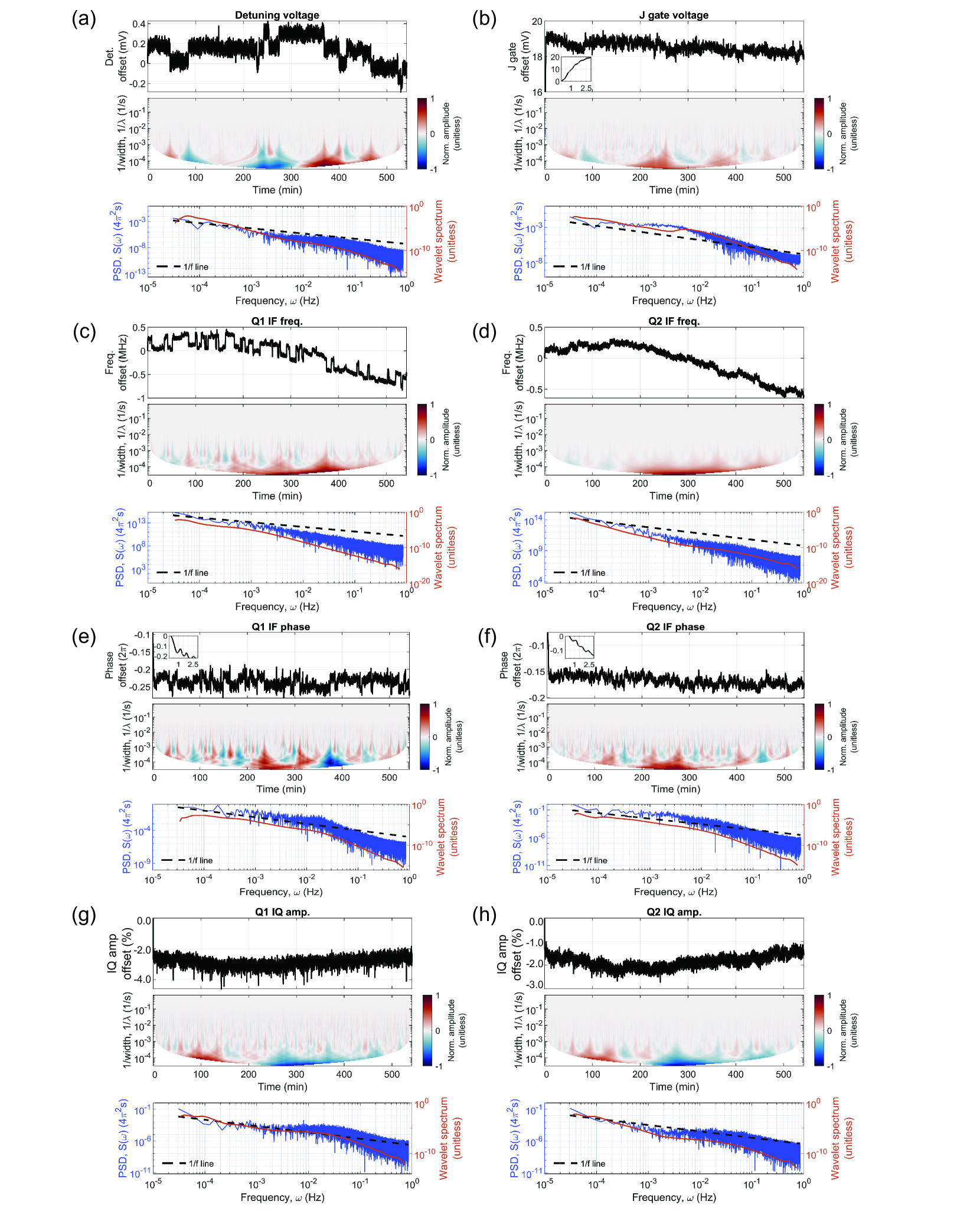
In this section we focus on the different features present in the data sets, and how they appear in the wavelet transformation. The feedback data in Fig. 2 shows several features which we categorise as: 1) discrete jumps, 2) slow drifts of low amplitude, and 3) small time-scale jumps.
The raw data shown in Fig 2(a), (b) and (c) features discrete jumps. The detuning voltage, Fig 2(a), shows a negative and positive shift at times 50 min and 90 min, respectively. To interpret these jumps in we recall that the wavelet transformation multiplies a Haar wavelet with the data at a particular and , Eq. 1. If the wavelet shape matches a feature in the data, is amplified, i.e. a good match between a data feature and the wavelet is shown as a high positive amplitude in . A data feature matching the inverse of the wavelet results in a high negative amplitude. The widths of the peaks at 50 min and 90 min increase as decreases until the width of the features starts overlapping. When high and low amplitude features meet they cancel to zero, shown as off-white in Fig. 2. Features with the same sign join and amplify . Examples in the detuning voltage shown in Fig 2(a) occur at 375 and 400 minutes, where two successive discrete jumps occur with the same sign, indicating that multiple two-level systems are involved. This is confirmed by the number of discrete levels seen in the detuning data which has four levels at detuning offset values of approximately 0.3 mV, 0.2 mV, 0 mV, and -0.1 mV. In comparison, data for Q1 IF frequency and IF phase feedback displayed in Fig 2(c) and (e) show fewer consecutive same-sign fluctuations, resulting in pattern of peaks with alternating sign in the wavelet transform at around 1/s.
It is thought that 1/f noise originates from ensembles of trapped two-level fluctuators, presumably in the dielectric material [23]. In this model, a single fluctuator contributes to the overall frequency spectrum following a Lorentzian distribution, manifesting itself in the Fourier PSD as a plateau followed by a 1/f2 trend starting at the fluctuator’s characteristic frequency. Fourier PSD shown in Fig. 2(c), (d) and (h) deviate from the 1/f trend and exhibit a bump at Hz, indicating a single, strongly coupled two-level fluctuator, or a more complex interplay of single and ensembles of two-level fluctuators[24]. While both the wavelet spectrum and Fourier PSD provide information on the characteristic frequency of the fluctuator, reveals more information of the dynamics of a fluctuator event in the time-domain.
Data presented in Fig 2(c) and (d) shows long timescale drifts which manifest in as high amplitude features at small values. For unidirectional drifts, has a constant sign at smaller values. An example can be seen in Fig. 2(d) where the main amplitude in remains positive below 1/s. For multi-directional drifts, such as the one seen in Fig. 2(g) and (h), shows both positive and negative amplitudes.
Persistent in all the feedback data are small amplitude, fast time-scale jumps. For example, the fast time-scale jumps in Fig. 2(a) have a standard deviation of approximately 0.05 mV, compared to the 0.2 mV standard deviation of the multi-level fluctuations discussed previously. The jumps resemble 1/f noise [25, 14] presenting itself as high frequency jumps occurring about the moving mean of the data and at smaller amplitudes than other features. The wavelet transformation shows these jumps as features at high with close to zero normalised amplitude. The PSD and wavelet spectra further confirm the presence of 1/frequency noise [24].
Another advantage of wavelets is their ability to compare signals at particular time-scales, aiding the characterisation of noise in the device. For example, similar features appear in in Fig 2(b) and (e) at 1/s and below. These insights help understanding important noise correlations within the system, a more rigorous correlation wavelet-based analysis is detailed in Ref. [12].
In conclusion, we present several FPGA-optimised feedback protocols to stabilise single- and two-qubit parameters for electron spin qubits formed in silicon quantum dots over a multi-hour timescale. We analyse the feedback data with a Haar wavelet transform, and compare the results with the Fourier PSD. Wavelet analysis shows evidence of several different noise signals, namely 1) discrete jumps, 2) slow drifts of low amplitude, and 3) small time-scale jumps. Further work will include analyses using different wavelet bases, including complex wavelets, and investigate correlations between the different qubit parameters. Such detailed breakdown of the noise signals can help to improve qubit fabrication processes and implement cost effective and scalable feedback protocols. These results demonstrate that FPGA-based qubit parameter tracking protocols and wavelet analyses are valuable tools to optimise qubit performance and characterise them against various noise sources.
Acknowledgements
We acknowledge support from the Australian Research Council (FL190100167 and CE170100012), the US Army Research Office (W911NF-23-10092), and the NSW Node of the Australian National Fabrication Facility. The views and conclusions contained in this document are those of the authors and should not be interpreted as representing the official policies, either expressed or implied, of the Army Research Office or the US Government. The US Government is authorised to reproduce and distribute reprints for Government purposes notwithstanding any copyright notation herein. A.E.S., S.S., and J.Y.H. acknowledge support from the Sydney Quantum Academy.
Data availability
The data that support the findings of this study are available from the corresponding author upon reasonable request.
Author contributions
W.H.L. and F.E.H. fabricated the devices, with A.S.D.’s supervision, on isotopically enriched 28Si wafers supplied by K.M.I.(800ppm). N.D.S., W.G., S.S., T.T., J.Y.H., and W.H.L. did the experiments, coding and initial analysis, with A.L., A.S., C.H.Y., and A.S.D.’s supervision. N.D.S. and A.E.S. did the feedback analysis. N.D.S. and A.E.S. wrote the manuscript, with the input from all authors.
References
- Noiri et al. [2022] A. Noiri, K. Takeda, T. Nakajima, T. Kobayashi, A. Sammak, G. Scappucci, and S. Tarucha, Nature Communications 2022 13:1 13, 1 (2022).
- Mills et al. [2022] A. R. Mills, C. R. Guinn, M. J. Gullans, A. J. Sigillito, M. M. Feldman, E. Nielsen, and J. R. Petta, Science Advances 8, 5130 (2022).
- Ma̧dzik et al. [2022] M. T. Ma̧dzik, S. Asaad, A. Youssry, B. Joecker, K. M. Rudinger, E. Nielsen, K. C. Young, T. J. Proctor, A. D. Baczewski, A. Laucht, V. Schmitt, F. E. Hudson, K. M. Itoh, A. M. Jakob, B. C. Johnson, D. N. Jamieson, A. S. Dzurak, C. Ferrie, R. Blume-Kohout, and A. Morello, Nature 2022 601:7893 601, 348 (2022).
- Tanttu et al. [2023] T. Tanttu, W. H. Lim, J. Y. Huang, N. D. Stuyck, W. Gilbert, R. Y. Su, M. Feng, J. D. Cifuentes, A. E. Seedhouse, S. K. Seritan, C. I. Ostrove, K. M. Rudinger, R. C. C. Leon, W. Huang, C. C. Escott, K. M. Itoh, N. V. Abrosimov, H.-J. Pohl, M. L. W. Thewalt, F. E. Hudson, R. Blume-Kohout, S. D. Bartlett, A. Morello, A. Laucht, C. H. Yang, A. Saraiva, and A. S. Dzurak, Stability of high-fidelity two-qubit operations in silicon (2023).
- Fowler et al. [2012] A. G. Fowler, M. Mariantoni, J. M. Martinis, and A. N. Cleland, Physical Review A 86, 032324 (2012).
- Vepsäläinen et al. [2022] A. Vepsäläinen, R. Winik, A. H. Karamlou, J. Braumüller, A. D. Paolo, Y. Sung, B. Kannan, M. Kjaergaard, D. K. Kim, A. J. Melville, and others, Nature communications 13, 1 (2022).
- Gilbert et al. [2023] W. Gilbert, T. Tanttu, W. H. Lim, M. Feng, J. Y. Huang, J. D. Cifuentes, S. Serrano, P. Y. Mai, R. C. C. Leon, C. C. Escott, K. M. Itoh, N. V. Abrosimov, H.-J. Pohl, M. L. W. Thewalt, F. E. Hudson, A. Morello, A. Laucht, C. H. Yang, A. Saraiva, and A. S. Dzurak, Nature Nanotechnology 18, 131 (2023).
- Blok et al. [2014] M. S. Blok, C. Bonato, M. L. Markham, D. J. Twitchen, V. V. Dobrovitski, and R. Hanson, Nature Physics 10, 189 (2014).
- Philips et al. [2022] S. G. Philips, M. T. Mądzik, S. V. Amitonov, S. L. de Snoo, M. Russ, N. Kalhor, C. Volk, W. I. Lawrie, D. Brousse, L. Tryputen, B. P. Wuetz, A. Sammak, M. Veldhorst, G. Scappucci, and L. M. Vandersypen, Nature 2022 609:7929 609, 919 (2022).
- Rojas-Arias et al. [2023] J. S. Rojas-Arias, A. Noiri, P. Stano, T. Nakajima, J. Yoneda, K. Takeda, T. Kobayashi, A. Sammak, G. Scappucci, D. Loss, and S. Tarucha, Spatial noise correlations beyond nearest-neighbor in 28si/sige spin qubits (2023).
- Percival and Walden [2000] D. B. Percival and A. T. Walden, Cambridge University Press (2000).
- Seedhouse and Dumoulin Stuyck [2023] A. E. Seedhouse and N. Dumoulin Stuyck, Manuscript in progress (2023).
- Almog et al. [2016] I. Almog, G. Loewenthal, J. Coslovsky, Y. Sagi, and N. Davidson, Physical Review A 94, 42317 (2016).
- Chan et al. [2018] K. W. Chan, W. Huang, C. H. Yang, J. C. C. Hwang, B. Hensen, T. Tanttu, F. E. Hudson, K. M. Itoh, A. Laucht, A. Morello, and A. S. Dzurak, Physical Review Applied 10, 44017 (2018).
- Guo et al. [2022] T. Guo, T. Zhang, E. Lim, M. Lopez-Benitez, F. Ma, and L. Yu, IEEE Access 10, 58869 (2022).
- Yang et al. [2020] C. H. Yang, R. C. C. Leon, J. C. C. Hwang, A. Saraiva, T. Tanttu, W. Huang, J. C. Lemyre, K. W. Chan, K. Y. Tan, F. E. Hudson, K. M. Itoh, A. Morello, M. Pioro-Ladrière, A. Laucht, and A. S. Dzurak, Nature 580, 350 (2020).
- Seedhouse et al. [2021] A. E. Seedhouse, T. Tanttu, R. C. C. Leon, R. Zhao, K. Y. Tan, B. Hensen, F. E. Hudson, K. M. Itoh, J. Yoneda, C. H. Yang, A. Morello, A. Laucht, S. N. Coppersmith, A. Saraiva, and A. S. Dzurak, PRX Quantum 2, 10303 (2021).
- Veldhorst et al. [2015] M. Veldhorst, C. H. Yang, J. C. Hwang, W. Huang, J. P. Dehollain, J. T. Muhonen, S. Simmons, A. Laucht, F. E. Hudson, K. M. Itoh, A. Morello, and A. S. Dzurak, Nature 526, 410 (2015).
- Veldhorst et al. [2017] M. Veldhorst, H. G. J. Eenink, C. H. Yang, and A. S. Dzurak, Nature Communications 8, 1 (2017).
- Vandersypen and Chuang [2004] L. M. K. Vandersypen and I. L. Chuang, Reviews of Modern Physics 76, 1037 (2004).
- Prance et al. [2015] J. R. Prance, B. J. Van Bael, C. B. Simmons, D. E. Savage, M. G. Lagally, M. Friesen, S. N. Coppersmith, and M. A. Eriksson, Nanotechnology 26, 215201 (2015).
- Haar [1911] A. Haar, Mathematische Annalen 71, 38 (1911).
- Hooge [2003] F. N. Hooge, Physica B: Condensed Matter 336, 236 (2003).
- Elsayed et al. [2022] A. Elsayed, M. Shehata, C. Godfrin, S. Kubicek, S. Massar, Y. Canvel, J. Jussot, G. Simion, M. Mongillo, D. Wan, B. Govoreanu, I. P. Radu, R. Li, P. Van Dorpe, and K. De Greve, arXiv preprint arXiv:2212.06464 (2022).
- Struck et al. [2020] T. Struck, A. Hollmann, F. Schauer, O. Fedorets, A. Schmidbauer, K. Sawano, H. Riemann, N. V. Abrosimov, Ł. Cywiński, D. Bougeard, and L. R. Schreiber, npj Quantum Information 6, 10.1038/s41534-020-0276-2 (2020).