Lateral Solid Phase Epitaxy of Yttrium Iron Garnet
Abstract
Solid phase epitaxy is a crystallization technique used to produce high quality thin films. Lateral solid phase epitaxy furthermore enables the realization of non-planar structures, which are interesting, e.g., in the field of spintronics. Here, we demonstrate lateral solid phase epitaxy of yttrium iron garnet over an artificial edge, such that the crystallization direction is perpendicular to the initial seed. We use single crystalline garnet seed substrates partially covered by a \chSiO_x film to study the lateral crystallization over the \chSiO_x mesa. The yttrium iron garnet layer retains the crystal orientation of the substrate not only when in direct contact with the substrate, but also across the edge on top of the \chSiO_x mesa. By controlling the crystallization dynamics it is possible to almost completely suppress the formation of polycrystals and to enable epitaxial growth of single crystalline yttrium iron garnet on top of mesas made from arbitrary materials. From a series of annealing experiments, we extract an activation energy of and a velocity prefactor of for the lateral epitaxial crystallization along the <> direction. Our results pave the way to engineer single crystalline non-planar yttrium iron garnet structures with controlled crystal orientation.
I Introduction
Epitaxy is one of the most commonly used techniques for obtaining single crystalline thin films. Stringfellow (1982); Evans et al. (2018) As a subset, solid phase epitaxy (SPE) describes the phase transition of an amorphous solid to its crystalline form while in contact with a crystalline seed of a similar or identical lattice parameter.Johnson et al. (2015) This causes the crystallization to start from the interface with the seed material and results in a single crystalline thin film of the same crystal orientation as the seed.Johnson et al. (2015)
A special type of SPE is lateral solid phase epitaxy (LSPE), where the crystallization direction is perpendicular to the initial seed surface normal. Ishiwara et al. (1983, 1986) Initially, lateral solid phase epitaxy was developed for the fabrication of silicon on insulator structures and has been an important technological step for the semiconductor industry. Ishiwara et al. (1983, 1986); Kusukawa et al. (1990); Hoefflinger (2011) Therefore, the SPE of silicon and germanium has been studied most comprehensively. Csepregi et al. (1976, 1977); Williams (1983); Johnson et al. (2008) Recently, the lateral crystallization of oxide thin films has gained increasing interest and has been shown for \chBa_0.6Sr_0.4TiO3,Lee and Joo (2000) \chNb:TiO2Taira et al. (2014) and \chSrTiO3. Chen et al. (2019)
In this paper we investigate the oxide compound yttrium iron garnet (\chY3Fe5O12, YIG). Its ferrimagnetic properties, Althammer et al. (2013) combined with a long spin diffusion length Kajiwara et al. (2010); Cornelissen et al. (2015) as well as an exceptionally low Gilbert damping and a low coercive field Chang et al. (2014); Hauser et al. (2016) make it a prototypical material in the field of magnetism and spintronics. Cherepanov et al. (1993)
In these areas the focus in recent years was expanded towards non-planar, three dimensional and curved magnetic structures Sanz-Hernández et al. (2017); Fernández-Pacheco et al. (2017); Heyroth et al. (2019); Lammel et al. (2022) as curvature was reported to induce novel phenomena like curvature-induced anisotropy Streubel et al. (2016) or the Dzyaloshinskii-Moriya-interaction. Dzyaloshinsky (1958) These phenomena in turn are predicted to lead to a variety of resulting effects, for example to spin-wave nonreciprocities Otálora et al. (2016); Salazar-Cardona et al. (2021) or magnetochiral effects.Dietrich et al. (2008); Sloika et al. (2014)
Realizing non-planar magnetic structures is therefore highly desirable. However, the deposition techniques commonly used for the fabrication of YIG like pulsed laser deposition and magnetron sputtering typically yield planar thin films.
In this work, we report the lateral solid phase epitaxy of YIG over an artificial mesa on top of crystalline seed substrates. From systematic annealing experiments, we extract the activation energy as well as the crystallization velocity which allow for a full description of the lateral solid phase epitaxy. Our results pave the way for experiments on more sophisticated non-planar structures of one of the prototypical magnetic materials for spintronics.
II Methods
All films discussed in this publication were deposited using radio-frequency magnetron sputtering at room temperature in an AJA International sputtering system.
For the lateral crystallization experiments, we used yttrium aluminum garnet (\chY3Al5O12, YAG, CrysTec) substrates with the <> crystal orientation being parallel to the surface normal as well as two types of gadolinium gallium garnet (\chGd3Ga5O12, GGG, SurfaceNet) substrates, where the crystal orientation along the surface normal is either <> or <>. Since GGG and YAG crystallize in the same space group Iad as YIG and their lattice parameters are comparable to those of YIG (aGGG = ,Gates-Rector and Blanton (2019a) aYAG = ,Gates-Rector and Blanton (2019b) aYIG = Gates-Rector and Blanton (2019c)) they are considered as closely lattice matched. Before the sputtering process all substrates were cleaned for five minutes in aceton and isopropanol, and one minute in deionized water in an ultrasonic bath.
To create an artificial mesa on the substrate surface, we first sputter a nominally thick \chSiO_x layer either from a \chSiO2 sinter target or by reactive sputtering from a silicon target onto one of the garnet substrates (cp. Fig. 1(a)). The \chSiO_x layer from the \chSiO_2 target (reactive Si) was deposited at a sputtering pressure of in pure argon atmosphere (argon to oxygen 13:4) at () at a rate of ().
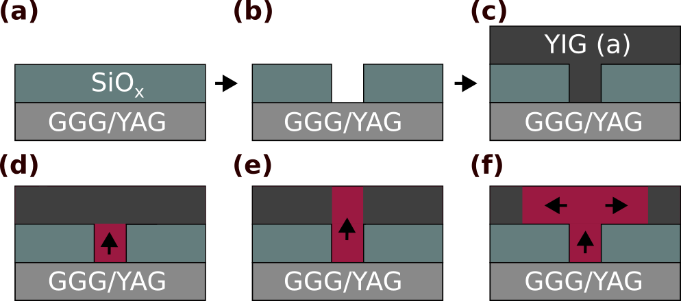
Several ways were utilized to fabricate the mesa from the \chSiO_x layer (cp. Fig. 1(b)). Some of the substrates were partially covered with Kapton tape before the \chSiO_x sputtering process, which yield the desired structure by simply removing the tape afterwards. While this path is simple, it leads to comparably rough edges. To improve the edge quality of the \chSiO_x mesa optical lithography and subsequent etching of the \chSiO_x was utilized. The form of the mesa was first defined in photoresist by a Smart Print (Smartforce Technologies) and after developing transferred into the \chSiO_x by physical etching with a \chSF6 plasma in an Oxford Instrument RIE system. To counteract any potential damage to the substrate after the etching step, it was annealed at for . We also used chemical etching of the \chSiO_x stripe in buffered \chHF.
In a subsequent fabrication step, we then deposit the YIG film on top of the predefined \chSiO_x mesas as sketched in Fig. 1(c). As we want to investigate lateral crystallization, the nominal YIG thickness was chosen to be at least twice as thick as the \chSiO_x to ensure continuity of the YIG layer across the mesa edge. YIG was sputtered from a stochiometric sinter target at argon pressure and power, at a rate of . This results in a complete coverage of the \chSiO_x mesas with YIG, where the YIG film within the predefined trench is still in contact with the lattice matched substrate (cp. Fig. 1(c)).
To induce and observe crystallization of the YIG layer, the complete stack was then annealed at temperatures between and multiple times in a tube furnace under air. The expected crystallization behavior upon annealing is shown in Fig. 1(d-f). First, YIG starts crystallizing vertically from the lattice matched substrate via solid phase epitaxy (cp. Fig. 1(d)). After reaching the top edge of the film, the epitaxial, single crystalline YIG now acts as a seed for the amorphous YIG on \chSiO_x (cp. Fig. 1(e)). Starting from the edge of the mesa a lateral crystallization front is expected to move with a constant velocity (cp. Fig. 1(f)). The evolution of crystalline YIG across the mesa was observed in an scanning electron microscope (SEM, Zeiss GeminiSEM), where the crystalline region was analyzed via electron backscatter diffraction (EBSD).
Transmission electron microscopy was conducted using a JEOL JEM F200 operated at acceleration voltage equipped with a GATAN OneView CMOS camera for fast imaging. Local EDS analysis was perfomed using a dual window-less silicon drift detector.
III Results and Discussion
The selection of the ideal annealing temperature is crucial for the observation of lateral crystallization. In our previous workSailler et al. (2023) we determined the parameters describing the vertical crystallization of YIG for different time and temperature pairs depending on the substrate. We demonstrated, that epitaxial crystallization from a lattice matched seed becomes possible at temperatures below those required for the formation of polycrystals. Vice-versa, the formation of polycrystalline YIG can be suppressed by using sufficiently low annealing temperatures. From our results we approximated, that for the formation of a fully polycrystalline film on \chSiO_x would take about . Avoiding the formation of polycrystalline grains is of great importance, as those would hinder the epitaxial crystallization. Please note that nucleation is a thermally activated process and therefore statistically also possible for lower temperatures. During our study we found that nucleation was more likely to occur if there were external nucleation sites in the form of particles on the respective sample, demonstrating the need of clean surfaces. However, the temperature for annealing has to be sufficiently high, since the crystallization rate depends exponentially on the temperature (cp. Eq. (1)). Below the crystallization via solid phase epitaxy of YIG will not occur in reasonable times (t >). Therefore, we are confined to a temperature range of about ( - ) to study the lateral crystallization of YIG.
Heyroth et al. Heyroth et al. (2019) showcased a single crystalline YIG bridge fabricated by coating a resist template with YIG deposited via pulsed laser deposition. After lift off the bridge is annealed at for . However, we do not expect their annealing process to be easily transferrable to larger, sputtered YIG structures, as we see significant formation of polycrystalline YIG above .
To mathematically describe the lateral solid phase epitaxy of YIG from a YIG seed we use a modified Arrhenius equation. Csepregi et al. (1975); Johnson et al. (2015) This description assumes a homogeneous crystallization front that moves through an amorphous material starting from a crystalline seed of the same material. At a given temperature , this crystallization front is expected to move with a constant velocity (). Here is the lateral crystallization velocity, the lateral crystallization distance and the annealing time. The crystallization velocity itself depends exponentially on the temperature as well as the activation energy and can be described by Eq. (1), Csepregi et al. (1975); Johnson et al. (2015)
| (1) |
where is the Boltzmann constant and the prefactor represents a maximal velocity.
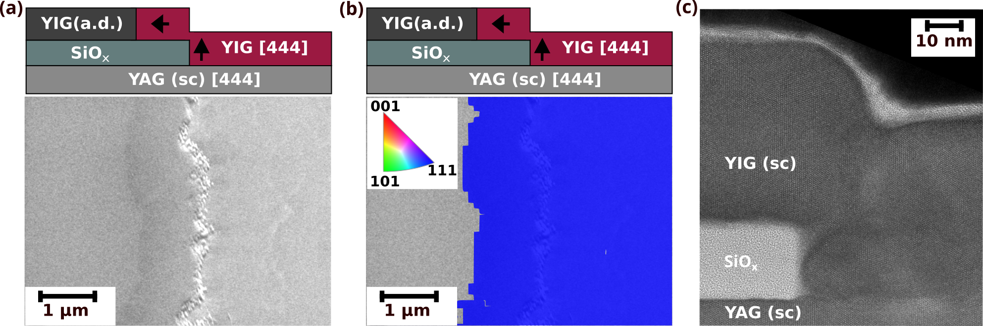
To confirm LSPE of YIG and to determine the crystallization velocities , we analyze our samples with electron back scatter diffraction (EBSD) for a sequence of annealing times. EBSD also allows us to exclude polycrystalline YIG on top of the \chSiO_x mesa. A secondary electron (SE) image taken across the edge of the mesa is depicted in Fig. 2(a). On the right, crystalline YIG is on top of the YAG substrate as depicted in the schematics above the SE image. The lateral crystallization front moves from the right across the mesa’s edge, which can be seen in the middle of the image, towards the left. The area of crystallized YIG on top of the \chSiO_x mesa can be discerned as a change in gray level which we ascribe to the height and density change upon crystallization.
To verify the formation of single crystalline YIG on YAG as well as across the mesa on \chSiO_x, the SE image is superimposed with the results from the EBSD mapping (cp. Fig. 2(b)). The monochrome color confirms a single crystalline YIG crystallizing in the same out of plane direction as the substrate. This demonstrates, that we achieved lateral solid phase epitaxy of YIG over a high mesa. Furthermore, unlike in similar studies on Si and other oxides, Ishiwara et al. (1983, 1986); Chen et al. (2019); Taira et al. (2014) we do not find any polycrystalline YIG seeds on \chSiO_x after at .
To further investigate the single crystalline nature of the laterally crystallized YIG, transmission electron microscopy (TEM) was performed. Fig. 2(c) depicts a side view of the mesa structure as illustrated schematically in Fig. 1(f) and Fig. 2(a + b). The TEM images show a sharp edge of the deposited \chSiO_x and a rounder YIG edge on top (Fig. 2(c)). The TEM image supports the results of the SEM investigation, in that the YIG layer crystallizes epitaxially from the substrate and also laterally on top of the \chSiO_x layer. However, close to the \chSiO_x edge in Fig. 2(c), some imperfections in the single crystal can be resolved in the TEM image. Additionally, a rotation of the crystal is visible, which results in a slightly tilted crystal on top of the \chSiO_x as the tilted YIG crystallizing from the bottom acts as the new seed for the lateral crystallization. This rotation is most clearly visible in samples where the direction is parallel to the surface normal and takes place exclusively in the planes perpendicular to the direction.
The distance up to which the YIG crystallizes laterally on top of the \chSiO_x can be extracted from both techniques, TEM and SEM. As the SEM allows for a fast measurement of the crystallization front, the lateral crystallization data is extracted from the SE images and EBSD data.
To determine the lateral crystallization velocities, each sample was annealed multiple times and the distance covered by the crystallization front was measured after each annealing step. At each time and temperature pair we analyze multiple images across the mesa edge and thereby obtain the respective, average crystallization distance and its standard deviation. We then determine the lateral crystallization velocity from the slope of a linear fit to the data. In addition to the rate, a temporal offset can be extracted. This offset occurs due to a delayed start of the lateral crystallization, which we assume is the time the YIG layer needs to crystallize vertically before being able to act as a seed. Furthermore, this temporal offset can stem from an initial induction period after which the velocity followed a linear rate, which has been reported for other materials. White et al. (1988)
Figure 3 shows the lateral crystallization velocity of YIG at when using <> oriented YAG and GGG as seed substrates. We extract a lateral crystallization velocity of = () for YIG on YAG and = () for YIG on GGG. On YAG the time delay before lateral crystallization is and on GGG .
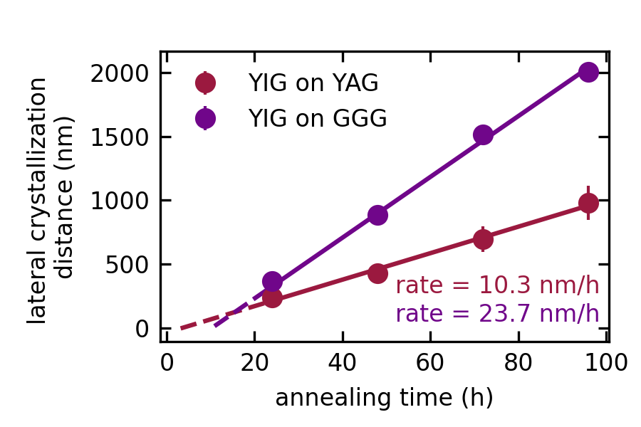
Since the lateral crystallization starts from a YIG seed for either of the substrates, one might expect the same lateral crystallization velocity. However, the different velocities suggest that the substrate indeed influences the maximal crystallization velocity. On the one hand, this behavior might originate from a different crystalline quality of the vertically crystallized YIG on the two substrates. Since GGG exhibits a lower lattice mismatch than YAG, it is expected to lead to a higher quality YIG film by epitaxy. On the other hand, the crystallization was not perfectly epitaxial near the \chSiO_x mesa (cp. Fig. 2(c)), which could influence the initial crystallization as well as the final velocity. In the course of this work we observed that the final velocity depends on surface and mesa edge quality.
To further substantiate our results, we compare our lateral crystallization velocity to the vertical crystallization velocity of YIG, which we reported in earlier work.Sailler et al. (2023) Compared to the vertical crystallization velocity of () for a YIG thin film on GGG, the lateral crystallization of YIG is five times slower on YAG and two times slower on GGG. Since the vertical crystallization of YIG on GGG was confirmed to be epitaxial, it allows for a good comparison with the LSPE of YIG. This behavior, that the lateral crystallization is slower than the vertical one, is naïvely unexpected but was also reported for silicon, where the lateral crystallization was four to eight times slower compared to the vertical direction.Ishiwara et al. (1983) In silicon this behavior was ascribed back to the formation of facets and defects in the lateral silicon.
Another reason for the slower lateral crystallization velocity could also be a dependence on the crystal direction along which the YIG crystallizes. From studies on silicon it is known, that differences in vertical crystallization velocity Csepregi et al. (1976, 1977) are transferred into the lateral crystallization. Kusukawa et al. (1990) Such a crystal orientation dependence of the crystallization velocities have also been reported for bulk YIG. Nielsen and Dearborn (1958); Erk et al. (1980); Tolksdorf and Bartels (1981)
Hence, to compare the lateral crystallization velocities extracted here with the ones from our previous work, that describe the vertical crystallization, the direction along which the crystallization takes place needs to be taken into account.111The direction of the lateral crystallization of the YIG layers from Fig. 3 can be identified to be , as it is perpendicular to and known from the substrate. There, the direction is parallel to the surface normal of the substrate, which is cut in a way to have one edge aligned parallel to the direction. The vertical crystallization on GGG took place along the direction.Sailler et al. (2023) Together with the different seed substrates, this direction dependence could play a role in the difference between the lateral crystallization velocity and the vertical one of a factor two for YIG on GGG.
In addition to the possibility of a direction dependence the lateral solid phase epitaxy of YIG is expected to exponentially depend on the temperature as described in Eq. (1).
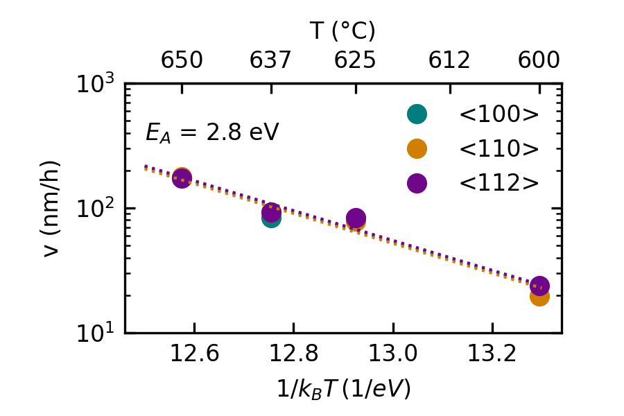
To investigate both the crystal orientation dependence and the temperature dependence, multiple samples were prepared on GGG substrates with the and directions parallel to the surface normal. These orientations allow for the investigation of the lateral crystallization velocity along the , , and directions. As YIG is a cubic system, these will be referred to as their equivalents <>, <> and <>. The crystallization along these directions was evaluated for samples annealed at different temperatures of , , and .
Although the formation of some polycrystalline grains could be seen with increasing temperature, this did not hinder the lateral crystallization up to a distance of via LSPE.
| Material | Ref | Orientation | (eV) | () |
|---|---|---|---|---|
| YIG | this work | <> | ||
| YIG | this work | <> | ||
| YIG | this work | <> | ||
| Si | CsepregiCsepregi et al. (1975) | <> | ||
| Si | CsepregiCsepregi et al. (1975) | <> | ||
| Ge | JohnsonJohnson et al. (2008) | <> | ||
| \ch SrTiO3 | WhiteWhite et al. (1988) | <> | 0.77 | |
| \ch SrTiO3 | ChenChen et al. (2017) | <> | 0.7 | |
Fig. 4 shows the results of these series over the annealing temperature. Each velocity shown in Fig. 4 is extracted from a series like the one shown in Fig. 3. From the semi-logarithmic plot, a linear dependence of the lateral crystallization velocity on the inverse temperature can be seen. As all the samples are made of the same material, i.e. YIG, we expect one single activation energy for all directions, Csepregi et al. (1975, 1977); Williams (1983); Johnson et al. (2008); Claverie et al. (2010) which we extract from the slope of a linear fit to all velocities. This results in an activation energy of = 2.8 for the lateral crystallization of YIG.
In contrast to the reports for the formation of bulk YIG,Tolksdorf and Bartels (1981) however, we find no significant difference in the maximal lateral crystallization velocity depending on crystal orientation. For the formation of bulk YIG from the liquid phase it was reported, that facets in <> and <> direction are the thermodynamically most stable, while the <> direction was described to grow fastest. Erk et al. (1980); Tolksdorf and Bartels (1981); Beregi et al. (1983) There, YIG was found to crystallize up to 10 times faster along the <> than along the <> direction, Erk et al. (1980) while the crystallization velocities along the <> and <> directions were found to behave very similarly. Tolksdorf and Bartels (1981)
For the LSPE of our sputtered thin films with an activation energy of we find prefactors of (<>) = , (<>) = and (<>) = . Tolksdorf et al. reported a very similar growth behavior of LPE grown YIG for facets along the <> and <> direction, with the <> direction being slightly faster, which we find here as well.Tolksdorf and Bartels (1981) No qualitative literature data could be found for the crystallization along the <> direction. Further studies involving a lateral growth along the faster crystallizing <> direction Erk et al. (1980); Tolksdorf and Bartels (1981) could help to verify a orientation dependence of lateral YIG growth.
Both the activation energies and the prefactors are in good agreement with the literature for solid phase epitaxy, see Tab.1. Compared to the model systems of silicon, germanium and \chSrTiO3, the activation energy for YIG is higher, while the crystallization velocities are in a similar order of magnitude as for silicon and germanium. The epitaxial crystallization process of YIG seems to be more similar to elemental Si and Ge than to the oxide \chSrTiO3.
Additionally, our activation energy of = for epitaxial YIG compares well with previously reported values. Specifically, investigations of YIG thin films on GGG revealed an activation energy of . Sailler et al. (2023) For the formation of bulk, polycrystalline YIG from oxide powders, a value of was reported. Wan Ali et al. (2016) Chen et al.Chen et al. (2017) report, that the activation energy for polycrystalline \chSrTiO3 is half of that of epitaxial \chSrTiO3, which is in good agreement with our findings for the YIG thin films. The activation energy for solid phase epitaxy of = is also roughly half of for the oxide powders and also reduced compared to the value of vertical crystallization on GGG substrates. We therefore conclude, that the lateral solid phase epitaxy of YIG is described by an activation energy of = and for the directions <>, <> and <> by the values of , and , respectively.
IV Conclusion
To assess the lateral solid phase epitaxy of YIG, we defined \chSiO_x mesa structures on top of single crystalline garnet substrates, which were subsequently covered by an amorphous YIG layer by room temperature sputtering. By carefully choosing the annealing temperature we were able to laterally crystallize up to of single crystalline YIG on top of an amorphous \chSiO_x layer. At on GGG a crystallization velocity of was found, which increased by a factor seven to at . By extracting multiple lateral crystallization velocities at different temperatures and along different crystal orientations, we confirmed an exponential dependence on temperature as expected for LSPE. The resulting crystallization parameters are summarized in Tab.1, where the crystallization velocity we derive is independent on the crystal orientation of the seed. The understanding of these dynamics allows for a controlled and precise manufacturing of single crystalline YIG thin films of micrometer length scales on arbitrary substrates and therefore pave the way for sophisticated non-planar structures.
V Acknowledgments
This work was funded by the Deutsche Forschungsgemeinschaft (DFG, German Research Foundation) – Project-ID 446571927 and via the SFB 1432 - Project-ID 425217212. We gratefully acknowledge technical support and advice by the nano.lab facility of the University Konstanz. We acknowledge the use of the facilities in the Dresden Center for Nanoanalysis (DCN) at the Technische Universität Dresden and the support of Alexander Tahn.
VI References
References
- Stringfellow (1982) G. B. Stringfellow, Rep. Prog. Phys. 45, 469 (1982).
- Evans et al. (2018) P. G. Evans, Y. Chen, J. A. Tilka, S. E. Babcock, and T. F. Kuech, Curr. opin. solid state mater. sci. 22, 229 (2018).
- Johnson et al. (2015) B. C. Johnson, J. C. McCallum, and M. J. Aziz, in Handbook of Crystal Growth (Elsevier, 2015) pp. 317–363.
- Ishiwara et al. (1983) H. Ishiwara, H. Yamamoto, S. Furukawa, M. Tamura, and T. Tokuyama, Appl. Phys. Lett. 43, 1028 (1983).
- Ishiwara et al. (1986) H. Ishiwara, M. Tanaka, and S. Furukawa, Appl. Phys. Lett. 49, 1363 (1986).
- Kusukawa et al. (1990) K. Kusukawa, M. Moniwa, M. Ohkura, and E. Takeda, Appl. Phys. Lett. 56, 560 (1990).
- Hoefflinger (2011) B. Hoefflinger, in Chips 2020, edited by B. Hoefflinger (Springer Berlin Heidelberg, Berlin, Heidelberg, 2011) pp. 161–174, series Title: The Frontiers Collection.
- Csepregi et al. (1976) L. Csepregi, J. W. Mayer, and T. W. Sigmon, Appl. Phys. Lett. 29, 92 (1976).
- Csepregi et al. (1977) L. Csepregi, R. Küllen, J. Mayer, and T. Sigmon, Solid State Commun. 21, 1019 (1977).
- Williams (1983) J. S. Williams, Nucl. Instrum. Methods Phys. Res. 209-210, 219 (1983).
- Johnson et al. (2008) B. C. Johnson, P. Gortmaker, and J. C. McCallum, Phys. Rev. B 77, 214109 (2008).
- Lee and Joo (2000) J.-S. Lee and S.-K. Joo, Jpn. J. Appl. Phys. 39, 6343 (2000).
- Taira et al. (2014) K. Taira, Y. Hirose, S. Nakao, N. Yamada, T. Kogure, T. Shibata, T. Sasaki, and T. Hasegawa, ACS Nano 8, 6145 (2014).
- Chen et al. (2019) Y. Chen, J. A. Tilka, Y. Ahn, J. Park, A. Pateras, T. Zhou, D. E. Savage, I. McNulty, M. V. Holt, D. M. Paskiewicz, D. D. Fong, T. F. Kuech, and P. G. Evans, J. Phys. Chem. C 123, 7447 (2019).
- Althammer et al. (2013) M. Althammer, S. Meyer, H. Nakayama, M. Schreier, S. Altmannshofer, M. Weiler, H. Huebl, S. Geprägs, M. Opel, R. Gross, D. Meier, C. Klewe, T. Kuschel, J.-M. Schmalhorst, G. Reiss, L. Shen, A. Gupta, Y.-T. Chen, G. E. W. Bauer, E. Saitoh, and S. T. B. Goennenwein, Phys. Rev. B 87, 224401 (2013).
- Kajiwara et al. (2010) Y. Kajiwara, K. Harii, S. Takahashi, J. Ohe, K. Uchida, M. Mizuguchi, H. Umezawa, H. Kawai, K. Ando, K. Takanashi, S. Maekawa, and E. Saitoh, Nature 464, 262 (2010).
- Cornelissen et al. (2015) L. Cornelissen, J. Liu, R. Duine, J. B. Youssef, and B. Van Wees, Nat. Phys. 11, 1022 (2015).
- Chang et al. (2014) H. Chang, P. Li, W. Zhang, T. Liu, A. Hoffmann, L. Deng, and M. Wu, IEEE Magn. Lett. 5, 1 (2014).
- Hauser et al. (2016) C. Hauser, T. Richter, N. Homonnay, C. Eisenschmidt, M. Qaid, H. Deniz, D. Hesse, M. Sawicki, S. Ebbinghaus, and G. Schmidt, Sci. Rep. 6, 20827 (2016).
- Cherepanov et al. (1993) V. Cherepanov, I. Kolokolov, and V. L’vov, Phys. Rep. 229, 81 (1993).
- Sanz-Hernández et al. (2017) D. Sanz-Hernández, R. F. Hamans, J.-W. Liao, A. Welbourne, R. Lavrijsen, and A. Fernández-Pacheco, ACS Nano 11, 11066 (2017).
- Fernández-Pacheco et al. (2017) A. Fernández-Pacheco, R. Streubel, O. Fruchart, R. Hertel, P. Fischer, and R. P. Cowburn, Nat. Commun. 8, 15756 (2017).
- Heyroth et al. (2019) F. Heyroth, C. Hauser, P. Trempler, P. Geyer, F. Syrowatka, R. Dreyer, S. G. Ebbinghaus, G. Woltersdorf, and G. Schmidt, Phys. Rev. Applied 12, 054031 (2019).
- Lammel et al. (2022) M. Lammel, D. Scheffler, D. Pohl, P. Swekis, S. Reitzig, S. Piontek, H. Reichlova, R. Schlitz, K. Geishendorf, L. Siegl, B. Rellinghaus, L. M. Eng, K. Nielsch, S. T. B. Goennenwein, and A. Thomas, Phys. Rev. Mater. 6, 044411 (2022).
- Streubel et al. (2016) R. Streubel, P. Fischer, F. Kronast, V. P. Kravchuk, D. D. Sheka, Y. Gaididei, O. G. Schmidt, and D. Makarov, J. Phys. D: Appl. Phys 49, 363001 (2016).
- Dzyaloshinsky (1958) I. Dzyaloshinsky, J. Phys. Chem. Solids 4, 241 (1958).
- Otálora et al. (2016) J. A. Otálora, M. Yan, H. Schultheiss, R. Hertel, and A. Kákay, Phys. Rev. Lett. 117, 227203 (2016).
- Salazar-Cardona et al. (2021) M. M. Salazar-Cardona, L. Körber, H. Schultheiss, K. Lenz, A. Thomas, K. Nielsch, A. Kákay, and J. A. Otálora, Appl. Phys. Lett. 118, 262411 (2021).
- Dietrich et al. (2008) C. Dietrich, R. Hertel, M. Huber, D. Weiss, R. Schäfer, and J. Zweck, Phys. Rev. B 77, 174427 (2008).
- Sloika et al. (2014) M. I. Sloika, V. P. Kravchuk, D. D. Sheka, and Y. Gaididei, Appl. Phys. Lett. 104, 252403 (2014).
- Gates-Rector and Blanton (2019a) S. Gates-Rector and T. Blanton, Powder Diffr. (PDF: 00-013-0493) 34, 352 (2019a).
- Gates-Rector and Blanton (2019b) S. Gates-Rector and T. Blanton, Powder Diffr. (PDF: 00-033-0040) 34, 352 (2019b).
- Gates-Rector and Blanton (2019c) S. Gates-Rector and T. Blanton, Powder Diffr. (PDF: 00-043-0507) 34, 352 (2019c).
- Sailler et al. (2023) S. Sailler, G. Skobjin, H. Schlörb, B. Boehm, O. Hellwig, A. Thomas, S. T. B. Goennenwein, and M. Lammel, “Crystallization Dynamics of Amorphous Yttrium Iron Garnet Thin Films,” (2023), arXiv:2308.00412 [cond-mat].
- Csepregi et al. (1975) L. Csepregi, J. Mayer, and T. Sigmon, Phys. lett., A 54, 157 (1975).
- White et al. (1988) C. White, L. Boatner, P. Sklad, C. McHargue, J. Rankin, G. Farlow, and M. Aziz, Nucl. Instrum. Methods Phys. Res. 32, 11 (1988).
- Nielsen and Dearborn (1958) J. W. Nielsen and E. F. Dearborn, J. Phys. Chem. Solids 5, 202 (1958).
- Erk et al. (1980) W. V. Erk, H. J. G. J. V. Hoek-Martens, and G. Bartels, J. Cryst. Growth 48, 621 (1980).
- Tolksdorf and Bartels (1981) W. Tolksdorf and I. Bartels, J. Cryst. Growth 54, 417 (1981).
- Note (1) The direction of the lateral crystallization of the YIG layers from Fig. 3 can be identified to be , as it is perpendicular to and known from the substrate. There, the direction is parallel to the surface normal of the substrate, which is cut in a way to have one edge aligned parallel to the direction. The vertical crystallization on GGG took place along the direction.Sailler et al. (2023).
- Chen et al. (2017) Y. Chen, M. H. Yusuf, Y. Guan, R. Jacobson, M. G. Lagally, S. E. Babcock, T. F. Kuech, and P. G. Evans, ACS Appl. Mater. Interfaces 9, 41034 (2017).
- Claverie et al. (2010) A. Claverie, S. Koffel, N. Cherkashin, G. Benassayag, and P. Scheiblin, Thin Solid Films 518, 2307 (2010).
- Beregi et al. (1983) E. Beregi, E. Sterk, F. Tanos, E. Hartmann, and J. Lábár, J. Cryst. Growth 65, 562 (1983).
- Wan Ali et al. (2016) W. F. F. Wan Ali, M. Othman, M. F. Ain, N. S. Abdullah, and Z. A. Ahmad, J. Am. Ceram. Soc. 99, 315 (2016).