Disorder and diffuse scattering in single-chirality (TaSe4)2I crystals
Abstract
The quasi-one-dimensional chiral compound (TaSe4)2I has been extensively studied as a prime example of a topological Weyl semimetal. Upon crossing its phase transition temperature CDW K, (TaSe4)2I exhibits incommensurate charge density wave (CDW) modulations described by the well-defined propagation vector (0.05, 0.05, 0.11), oblique to the TaSe4 chains. Although optical and transport properties greatly depend on chirality, there is no systematic report about chiral domain size for (TaSe4)2I. In this study, our single-crystal scattering refinements reveal a bulk iodine deficiency, and Flack parameter measurements on multiple crystals demonstrate that separate (TaSe4)2I crystals have uniform handedness, supported by direct imaging and helicity dependent THz emission spectroscopy. Our single-crystal X-ray scattering and calculated diffraction patterns identify multiple diffuse features and create a real-space picture of the temperature-dependent (TaSe4)2I crystal structure. The short-range diffuse features are present at room temperature and decrease in intensity as the CDW modulation develops. These transverse displacements, along with electron pinning from the iodine deficiency, help explain why (TaSe4)2I behaves as an electronic semiconductor at temperatures above and below CDW, despite a metallic band structure calculated from density functional theory of the ideal structure.
I Introduction
Materials with nontrivial topological band structures represent an exciting frontier for exotic physics and quantum materials applications Wieder et al. (2022). Topological insulators show strong spin-orbit coupling leading to inverted and gapped electronic bands, resulting in topologically protected metallic surface states and insulated bulk states Fu et al. (2007); Moore and Balents (2007); Qi and Zhang (2011); Kumar et al. (2021); Hasan and Kane (2010); Moore (2010); B. A. Bernevig and Hughes (2013). Some electronic structures with similar band inversion may still retain isolated band crossings; such materials are known as Weyl or Dirac semimetals Wan et al. (2011); Yan and Felser (2017); Narang et al. (2021); Kumar et al. (2021). Much attention has recently fallen on the quasi-one-dimensional chiral charge density wave (CDW) material (TaSe4)2I, a prototype Weyl semimetal. (TaSe4)2I belongs to a class of materials characterized by exotic Fermi arc topological surface states and Weyl fermions within the bulk Shi et al. (2021); Weyl (1929); Wan et al. (2011); Potter et al. (2014); Xu et al. (2015); Jia et al. (2016); Hasan et al. (2017). Weyl fermions are massless quasi-particles that manifest themselves as low-energy excitations of the Weyl semimetal; when at zero energy, these quasi-particles correspond to degenerate band crossings found near the Fermi surface where the momentum dispersion is approximately linear in all three dimensions, serving as a 3D analog to 2D materials like graphene Castro Neto et al. (2009). Known as Weyl nodes, these band crossings occur as pairs with opposite chirality, requiring either time-reversal symmetry or inversion symmetry to be broken Weng et al. (2015). Weyl node pairs, with their opposite topological charges, act as sources (monopoles) and sinks (antimonopoles) for Berry curvature B. A. Bernevig and Hughes (2013), and their separation in momentum space provides a topologically protected phase Liu and Vanderbilt (2014); Hasan et al. (2017).
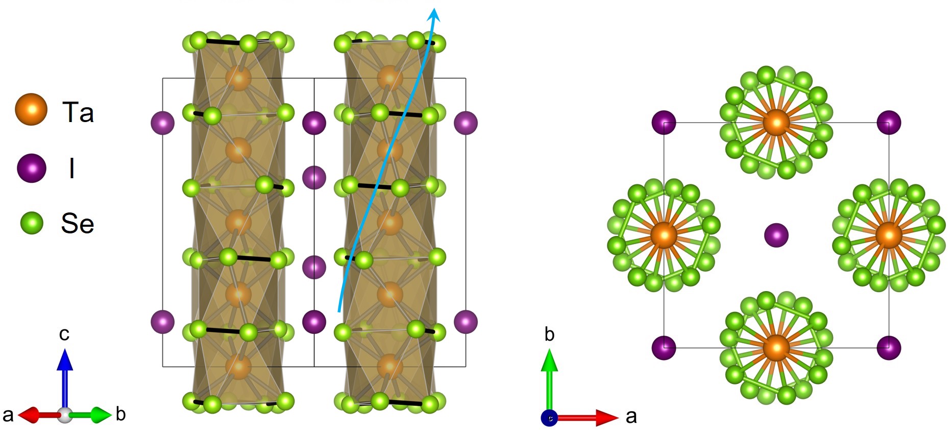
The structural properties of (TaSe4)2I were first published decades ago Gressier et al. (1982, 1984). At high temperature, chiral (TaSe4)2I crystallizes in the tetragonal space group with each body-centered unit cell consisting of two parallel TaSe4 chains, where each Ta ion is 8-coordinated by a pair of Se4 rectangles, while each rectangle contains a pair of dimers. These equally-spaced chains are separated by a row of four iodine ions as shown in Fig. 1. The orientation of Se imparts a chiral handedness. Topological semimetals lacking mirror symmetry in this manner are theorized to display many unusual optical, magnetic, and transport properties Jia et al. (2016); Zhong et al. (2016); Sanchez et al. (2019); Schröter et al. (2019) absent in centrosymmetric semimetals, such as helicity dependent currents produced through the circular photogalvanic effect (CPGE)Asnin et al. (1979); Belinicher and Sturman (1980); de Juan et al. (2017); Rees et al. (2020), a phenomenon leveraged in this paper.
(TaSe4)2I enters an incommensurate CDW state at the transition temperature CDW K, commonly detected by an anomaly in electrical resistivity.Maki et al. (1983); Wang et al. (1983) Weyl semimetals may be gapped out when Weyl nodes are spontaneously removed through pair annihilation between fermions and holes, creating a less-explored topological configuration known as an axionic insulator in tandem with a CDW Wang and Zhang (2013); Sekine and Nomura (2021). Although evidence has been proposed for this behavior in (TaSe4)2I Gooth et al. (2019), it is not entirely clear if the CDW phase is a direct result of chiral symmetry breaking in this mannerSinchenko et al. (2022). In general, the metallic state in one-dimensional systems similar to (TaSe4)2I is unstable, prone to breaking symmetry by formation of spin or charge density wave phases Grüner (2019). The (TaSe4)2I CDW phase is often described as Peierls-like in nature Voit et al. (2000). According to this picture, distortions are induced by electronic instabilities originating from Fermi surface nesting found in quasi-1D systems Monceau (2012); Tournier-Colletta et al. (2013). Previous (TaSe4)2I band structure studies also lend to this Gressier et al. (1984); Zhang et al. (2020). But detailed X-ray and neutron scattering analyses have revealed a more complicated modulation than a textbook one-dimensional Peierls instability: broken symmetry is indeed found along the chain direction as a Ta-tetramerization, but strong acoustic modulations form perpendicular to both the chain direction and the modulation wavevectors Lee et al. (1985); Lorenzo et al. (1998); Smaalen et al. (2001); Favre-Nicolin et al. (2001). Ascertaining the true structural and electronic behavior of the CDW phase is challenging due to incommensurability, but calculation of the band structure of a model (TaSe4)2I cell with Ta displacements by Tournier-Colletta, et al.Tournier-Colletta et al. (2013) confirmed the creation of a gap near , which they correlate with angle-resolved photoemission spectroscopy (ARPES) data. This was only done at 100 K, so the possible absence of a gap at high temperature was not examined. The semiconductor-like transport at high temperatures was conjectured to occur due to polaron hopping from the iodine vacancies Tournier-Colletta et al. (2013).
In the above studies, substantial work on structural characterization and transport has been performed, while the ultimate goal of helicity-dependent transport and optical excitation requires operation on a domain of (TaSe4)2I with single chirality (one enantiomer). The challenge of determining enantiopurity in a dense, opaque material can be addressed by multiple methods. Here we obtain both chirality and occupancy information from an extensive set of single-crystal X-ray refinements which reveal a consistent, intrinsic iodine deficiency within bulk (TaSe4)2I. The handedness of the refinements suggest that each (TaSe4)2I crystal tends to form with uniform handedness, which is affirmed by annular dark field scanning transmission electron microscopy (ADF-STEM) images and measurements of the circular photogalvanic effect. Synchrotron single-crystal X-ray diffraction (XRD) measurements above and below the CDW transition reveal organized diffuse scattering, often with a strong component in the -plane, confirming the strong effects between chemical disorder and the CDW transition in (TaSe4)2I. The source and nature of (TaSe4)2I diffuse scattering is investigated through scattering calculated from discrete atomic models.
II Methods
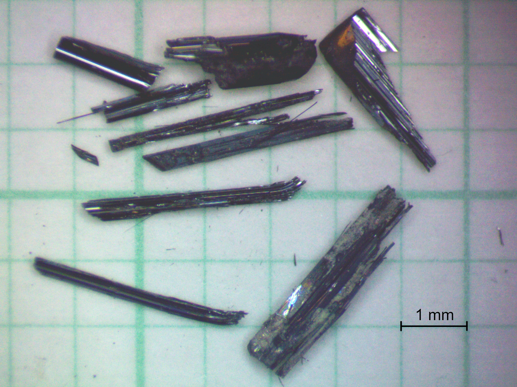
Single crystals of (TaSe4)2I were grown with a recipe similar to what was described by Maki, et al. Maki et al. (1983) Stoichiometric amounts of iodine granules (Fisher, 99.99%), selenium powder (Alfa Aesar, 99.999%), and tantalum wire (Fisher, 99.95%) were loaded and sealed in 15 mm diameter evacuated quartz tubes along with an excess of iodine to balance the loss of iodine during sample handling. A thermal gradient of 600 ∘C to 500 ∘C was applied for 10 days, producing black, thin crystals up to 12 mm in length and up to 2 mm in width, with typical dimensions being mm3. Smaller reaction tubes and tantalum powder were also used, but the crystals were not as large as those grown in the way reported above. Crystal images are shown in Fig. 2. A powder XRD fit is provided in the Supplemental Material (Fig. S3)sup .
For our diffuse scattering investigations, single-crystal reciprocal space scattering maps were obtained at the Advanced Photon Source (APS) beamline 6ID-D using a beam energy of 64.8 keV in a transmission geometry. The (TaSe4)2I sample with a diameter of about 0.3 mm was mounted on the tip of a Kapton capillary. A Pilatus 2M CdTe detector placed at a distance of 125.6 cm from the sample was used to collect energy-integrated images with higher dynamic range than our in-lab source described in the following paragraph. Sample temperatures were controlled between 30 and 300 K using a Oxford N-HeliX Cryostream. The raw images were pre-processed with a peak-finding algorithm to determine and refine the orientation matrix and then rebinned with a bin size of rlu into a reciprocal space volume rlu using the CCTW reduction workflow Krogstad et al. (2020); Jennings (2016).
To track the chirality trends of the material, additional room temperature data were collected on a Bruker D8 Venture diffractometer equipped with a Photon-II CPAD detector and Kappa goniometer. An Iµs microfocus Mo source ( = 0.71073 Å) coupled with a multi-layer mirror monochromator provided the incident beam. The sample was mounted on a 0.3 mm nylon loop with a minimal amount of Paratone-N oil. A single 180° -scan was collected for each crystal fragment with 1° frame angles. The collection, cell refinement, and integration of intensity data were carried out with the APEX3 software and SHELXL Sheldrick (2015). Multi-scan absorption corrections were performed with SADABS2.
Specimens of (TaSe4)2I were prepared for ADF-STEM using focused ion beam lift-out and milling (micrographs provided in Fig. S4 of the Supplemental Material sup ). Imaging was performed using an aberration-corrected STEM (Thermo Fisher Scientific Themis Z) operated at 300 kV, with 18 mrad convergence semiangle and 30 pA probe current. Individual frames were acquired with dwell time of 1 s and pixel size of 8.7 pm, and 10-50 frames were averaged to produce the final images.
THz emission spectroscopy was performed using a custom built time-domain THz spectroscopy setup based on a Yb:KGW amplifier laser (PHAROS, Light Conversion). The fundamental laser pulse wavelength is 1030 nm with a pulse duration of 160 fs. The fundamental beam is split into pump and probe paths using a 90:10 beamsplitter. The pump had a 1/e2 width of 1 mm on the sample at a 45° angle of incidence. The THz field radiated by the sample is collected by an off-axis parabolic mirror and focused on a CdTe (110) crystal. The electro-optical sampling probe beam is made to spatially and temporally overlap with on the CdTe crystal for electro-optic sampling. The path length of the probe is adjusted with a delay stage to control the time delay .
All lattice models and diffuse scattering were simulated using the DISCUS software suite Proffen and Neder (1997, 1999); Neder and Proffen (2008), applying both periodic displacement and density modulations. The scattering was simulated on lattices built with the standard (TaSe4)2I unit cell displayed in Fig. 1. The extent and resolution of the simulated reciprocal space was adjusted to avoid finite size effects (see Supplemental Material sup for more details). For most of our results the reciprocal volume was set to rlu with 200 points along each axis. All diffuse scattering simulations were calculated using MoK X-rays ( = 0.71073 Å) and with both atomic displacement parameters and anomalous dispersion turned off.
III Results and Discussion
III.1 Single-crystal structural refinement
Sample Handedness GooF Flack Occupancy 1 left 1.149 0.017(26) 0.886(22) 2 left 1.071 -0.012(74) 0.888(50) 3 left 1.073 0.015(24) 0.882(24) 4 left 1.235 0.021(15) 0.873(53)
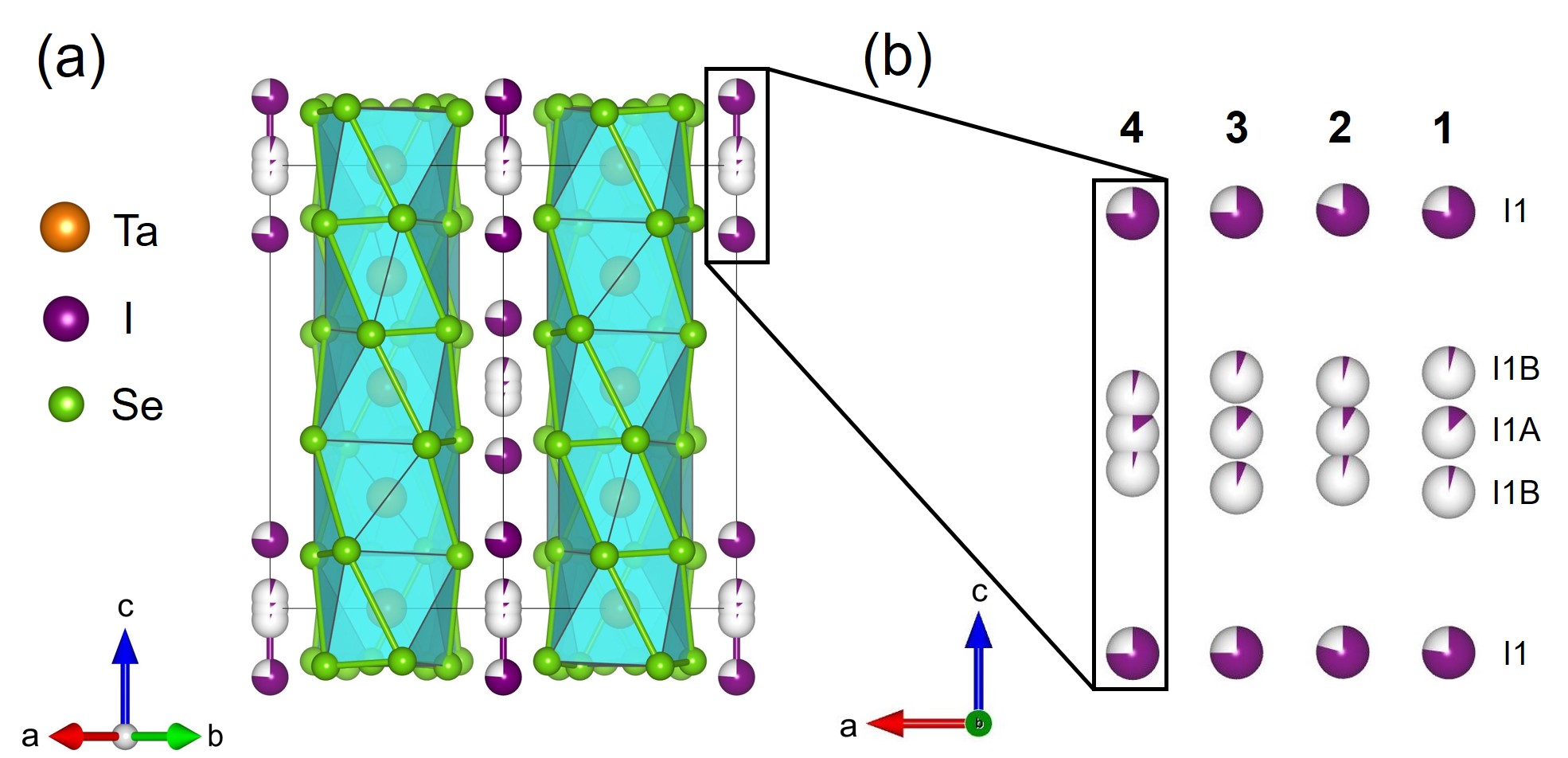
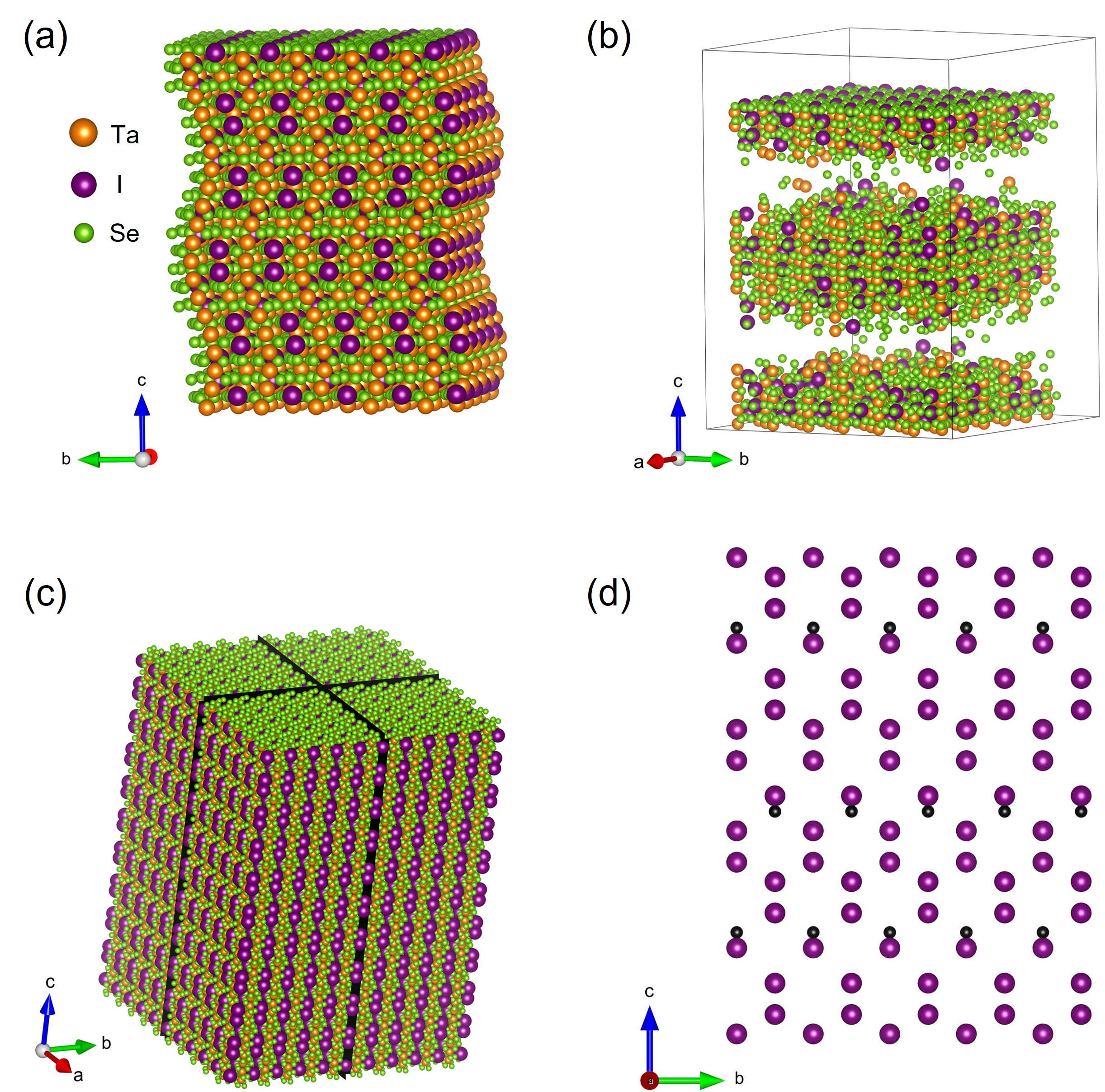
Our single-crystal XRD confirms the presence of a bulk iodine deficiency in our samples. Refinement parameters from four different full X-ray data sets are given in Table 1 (with additional detailed parameters for sample 3 found in the Supplemental Material sup , Tables S2 and S3), while Fig. 3 displays examples of the unit cells. Although the exact occupancies varied from crystal to crystal, the overall deficiency remained relatively consistent with a weighted average of approximately 0.88(2) total iodine fractional occupancy. Figure 3(a) shows the unit cell refinement from sample 4 of Table 1 with the associated occupancy information displayed as fractional atomic spheres. Figure 3(b) shows four iodine chains from each of the four crystals stacked next to one another, demonstrating the slight variation between refinements for position and fractional occupancy. Refinements 1 and 2 are separate crystals at room temperature, while refinements 3 and 4 are the same crystal examined at room temperature and = 100 K, respectively. For sample number 4, the regular iodine I1 position gives the highest occupancy of 0.756(6). The I1A site gives an occupancy of 0.14(6), and the I1B site gives an occupancy of 0.05(3). Details about the crystal refinement process are given in the Supplemental Material sup .
This iodine deficiency is likely related to the electrical resistance of (TaSe4)2I, which is well-documented in the vicinity of the CDW temperature Maki et al. (1983); Wang et al. (1983); Forró et al. (1987); Gooth et al. (2019), and later found to contain a semiconductor-semiconductor phase transition Tournier-Colletta et al. (2013); Kim et al. (2021). Below the transition temperature, the observed temperature dependence is not unexpected due to the opening of band gaps. Above the transition temperature, however, the (TaSe4)2I resistance is in stark contrast to the DFT-calculated band structure of the ideal, high-temperature structure, which places the Fermi level above the Weyl nodes, seeming to imply metallic conductivity. Previous studies stress the importance of the electron-phonon interaction in (TaSe4)2I as a basis for this resistivity behavior Crepaldi et al. (2022); Perfetti et al. (2001). Vacancies from the iodine deficiency have also been proposed to underlie this discrepancy, along with transverse displacements of Ta ions.Tournier-Colletta et al. (2013) Both could lead to the observed transport behavior. The iodine vacancies likely contribute to the high-temperature disorder that we explore in Section III.5.
With an understanding of the intensity distribution of a scattering pattern, we can determine if our material contains a chiral domain boundary. Friedel’s law dictates the existence of indistinguishable points within reciprocal space known as Friedel pairs, points with inverted phase but identical amplitudes. If a crystal has centrosymmetric symmetry the Friedel pairs will have exactly the same amplitudes. When symmetry is broken, the Bragg reflection positions are not altered. Instead, the intensities of Friedel points differ when dynamical absorption effects are considered in crystals containing species of differing atomic numbers. This distinction is utilized in the calculation of the Flack parameter Flack (1983); Flack and Bernardinelli (2008); Parsons et al. (2013); Watkin and Cooper (2020); Valentín-Pérez et al. (2022), a refinement factor used for determining chirality and given in the form
| (1) |
where is the calculated structure factor, is the structure factor for the inverted phase, is the observed structure factor, and is the Flack parameter. The Flack parameter quantifies the correctness of a refinement’s absolute structure, reported as a fraction between 0 and 1. A value of 1 indicates a structure which is fully inverted from its correct configuration (), while a value of 0 indicates the proper configuration with no inversion (). Intermediate values represent different fractions of inversion twinning. For example, a Flack parameter which converges to around 0.5 would suggest the crystal in question has a mixture of 50% left handed and 50% right handed configurations.
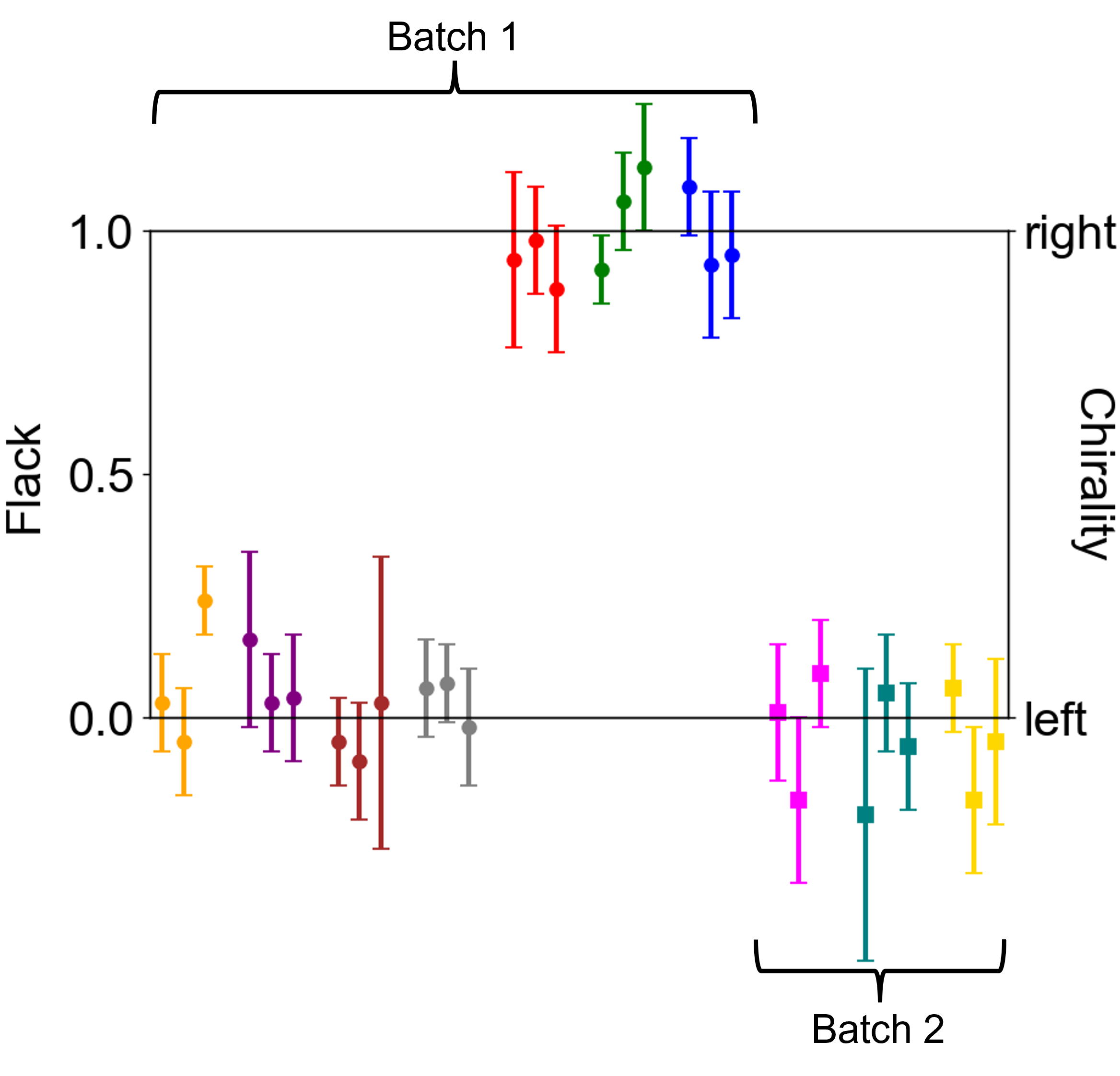
A previous study from Yi, et al.Yi et al. (2021) reported (TaSe4)2I chirality trends through the use of the Flack parameter in their Supplemental Material. Only one Flack parameter was reported with a value of 0.3(1), which may suggest inversion twinning. This value was an average value for an undisclosed number of crystals tested by the group. To build upon this work and provide a clearer picture of the (TaSe4)2I chirality trends, we present additional, more detailed studies of the size and distribution of chiral domains through structure refinements done on several locations across multiple large (millimeter-scale) crystals. A total of 10 crystals were tested from two synthesis batches. The crystals were too large to be examined in their as-grown state so the crystals were cut into several pieces. When cut, the crystals delaminate into very thin needles. Three needles from each large crystal were examined for intensity data – one from each end of the crystal and one from the middle section of the crystal for a total of 30 specimens. The resulting integrated intensities were refined against the atomic positions of a reference (TaSe4)2I crystal (sample 3 from Table 1), giving us 30 different Flack parameters. A full scattering data set was previously collected on the reference crystal, showing excellent refinement statistics (see Tables S2 and S3 in the Supplemental Material sup ) along with a Flack parameter which converges to near zero, indicating single chirality. Because the reference crystal has a known handedness, refining against this crystal will determine each crystal fragment’s handedness with respect to the handedness of the reference crystal. A similar method was used by di Gregorio, et al.di Gregorio et al. (2020) In this circumstance, a Flack parameter of 0 indicates a crystal fragment with the same handedness (left) as the reference crystal, and a value of 1 indicates a crystal with opposite handedness (right). The resulting data can be viewed in Fig. 4; additional refinement parameters can be found in Table S4 of the Supplemental Material sup . We found that handedness remained consistent within each crystal, save a few higher uncertainties in measurement; that is, all three pieces from a single crystal shared the same, uniform handedness. However, handedness was observed to vary among separate crystals.
III.2 Electron microscopy
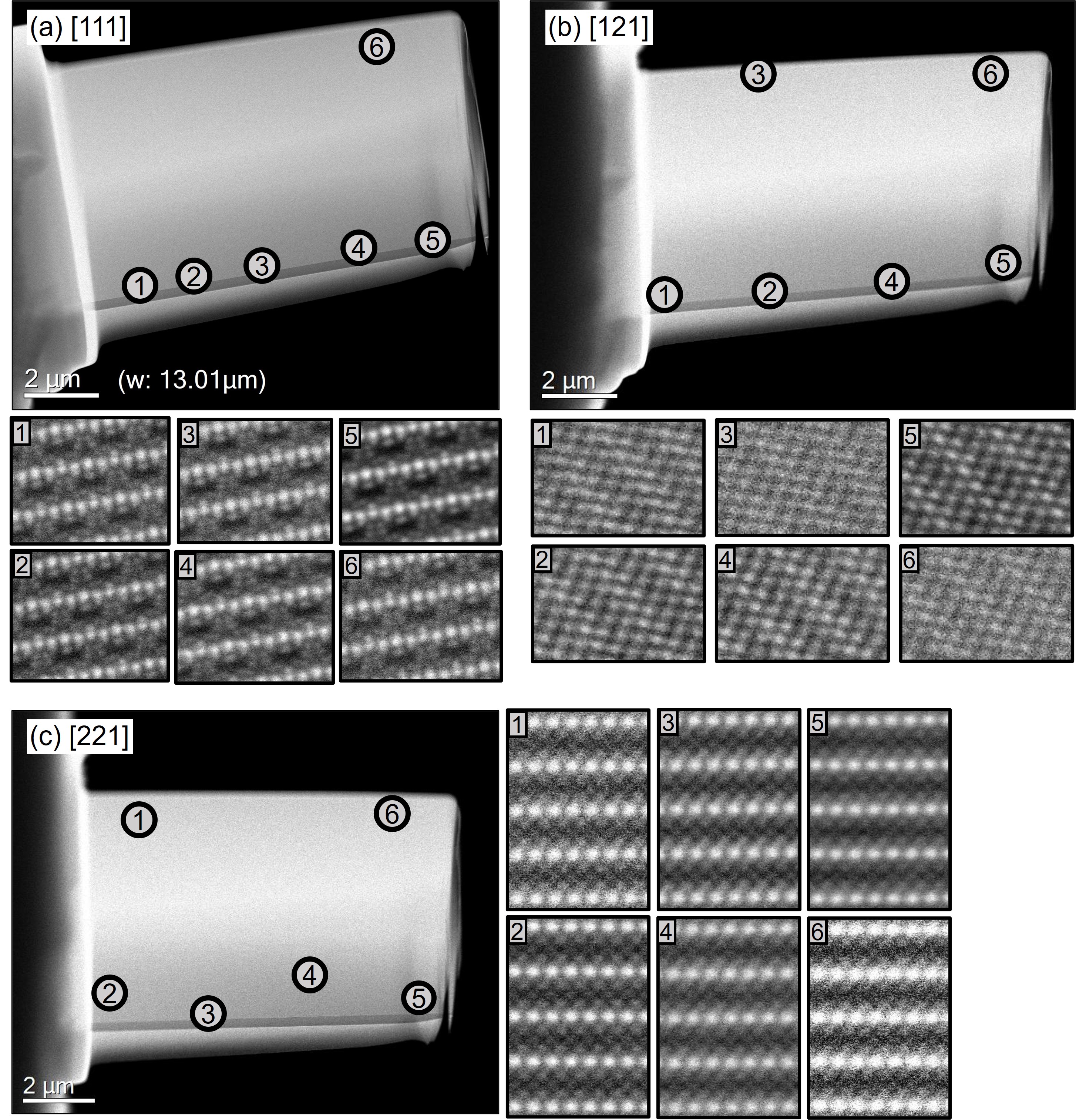
Single-crystal XRD enantiopurity is supported by ADF-STEM atomic resolution imaging of a (TaSe4)2I crystal, shown in Fig. 5. Because STEM images are two-dimensional projections, determining the chirality of a sample via STEM requires imaging from multiple zone axes Dong and Ma (2020). Therefore, ADF-STEM images were acquired of the same grain of (TaSe4)2I from the four zone axes [111], [121], [112], and [121]. Then, for each orientation the (TaSe4)2I crystal was imaged at six different locations which covered a range of roughly 10 m. Orientations were observed to vary by no more than 4° from one another. We attribute this variation to twisting caused by the sample preparation process. Otherwise, all images from their respective zone axes show resolvable, well-stacked, and non-rotated (TaSe4)2I chains. This indicates single chirality over depth (tens of nm) and breadth within the crystal tested.
III.3 Optical chiral response
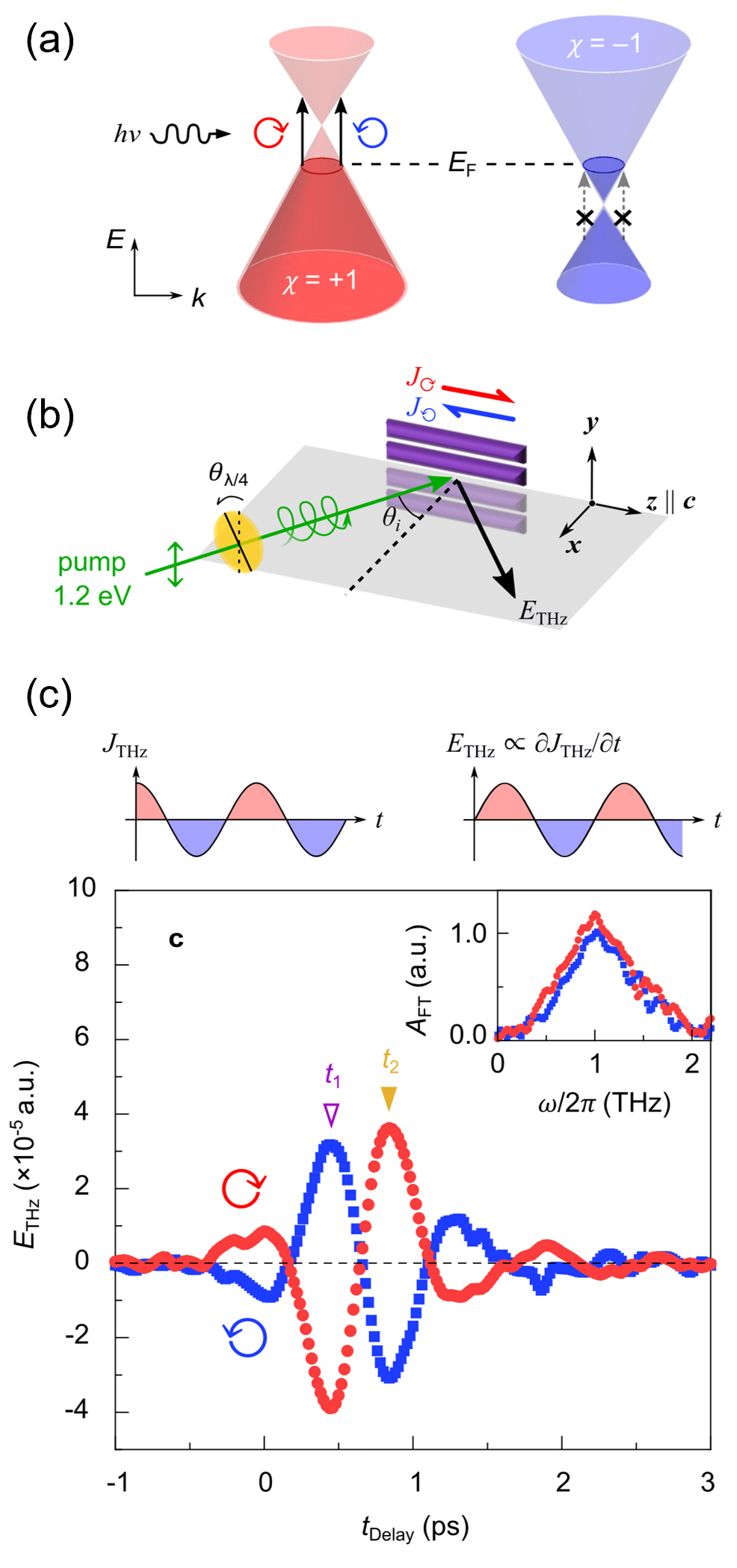
A third confirmation for the consistency of structural chirality in (TaSe4)2I is provided through measuring circular photogalvanic effects (CPGE) using THz emission spectroscopy with a circularly polarized pump Sturman and Fridkin (1992). Since (TaSe4)2I is structurally chiral but non-magnetic (preserves time-reversal symmetry), it naturally contains Kramers-Weyl fermions as illustrated in Fig. 6(a) Chang et al. (2018). In such systems, a photogalvanic current can be generated using circularly polarized light. Crucially, opposite helicities of light (right vs. left) will produce currents in opposite directions provided the sample has a constant chirality over the spot size of the light Rees et al. (2020). A contact-free method to measure CPGE is THz emission spectroscopy whereby a short duration IR pulse generates a transient current which emits THz radiation in the far-field (Fig. 6(b)). The emitted THz can be measured in the time-domain using standard electro-optic sampling (EOS) methods. The change in the phase of the emitted THz upon change in light helicity indicates non-zero CPGE. Figure 6(c) shows the THz emission signal as a function of EOS delay on (TaSe4)2I for right and left circularly polarized light. The 1.2 eV light was incident upon the sample at an incidence angle of 45° with a spot size of approximately 1 mm. As can be seen, opposite helicities of light result in opposite phases of the EOS signal indicating a circular photogalvanic effect and confirms the constant structural chirality of (TaSe4)2I over the 1 mm laser spot size.
III.4 Modeling the CDW phase
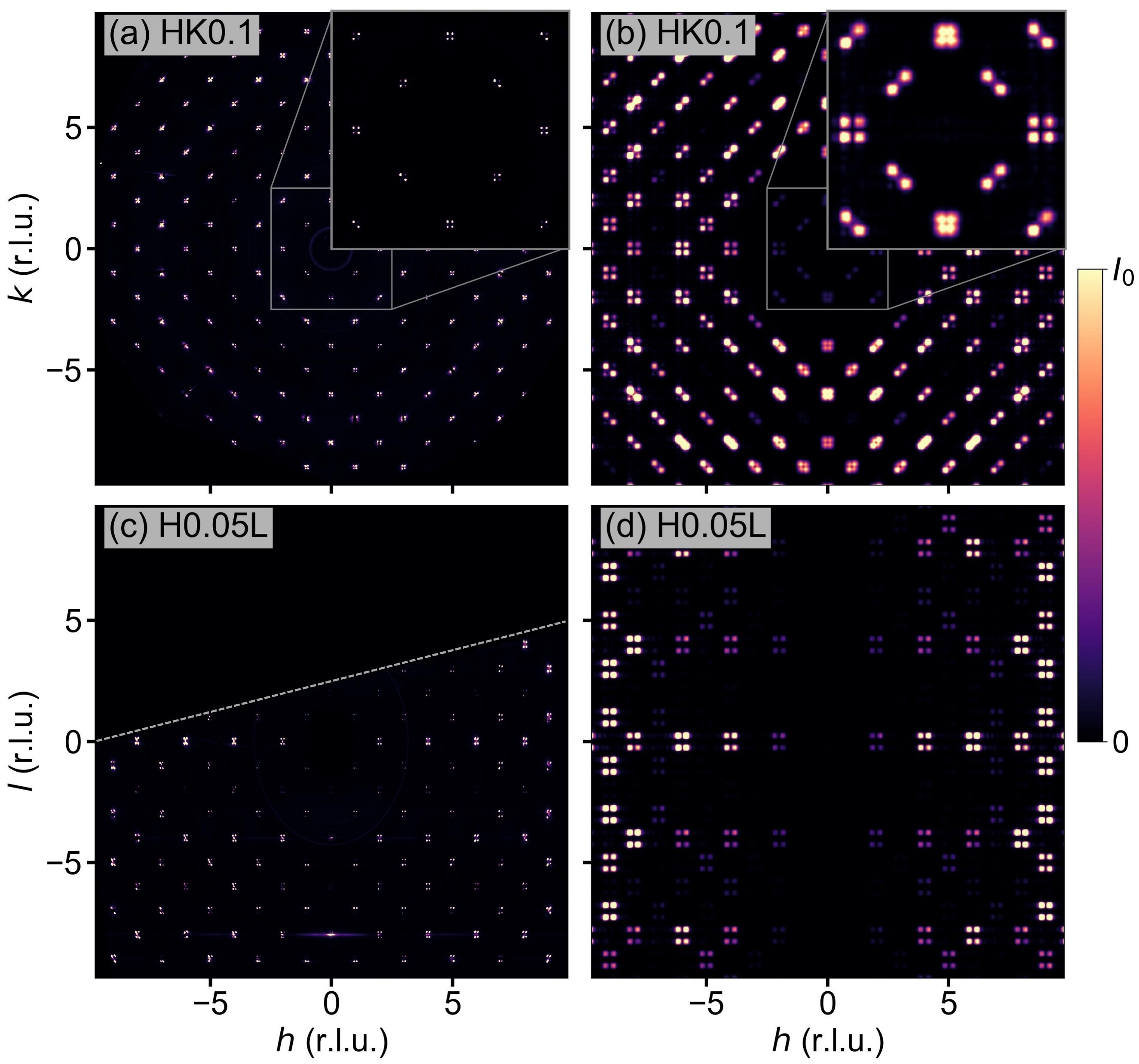
The single-crystal synchrotron XRD with high dynamic range and better q resolution shows an interesting assortment of diffuse scattering. First-order satellite peaks caused by the CDW phase are readily apparent below the transition temperature. These well-known peaks appear near the Brillouin zone centers in a tetragonal assembly defined by the eight locations ) rlu, with the main Bragg reflection set as the reference point Fujishita et al. (1985, 1984). Previous studies have found values ranging from 0.027 to 0.05 for and 0.012 to 0.151 for Fujishita et al. (1986); Shi et al. (2021); Smaalen et al. (2001); Lee et al. (1985); Yi et al. (2021); Favre-Nicolin et al. (2001). For our crystal, we report numbers of and . Lee, et al. speculates the discrepancy in the measured wavevector among studies is correlated with variations in the iodine deficiency of each (TaSe4)2I crystal Lee et al. (1985). This remains an open question, but our measurements of large deficiencies among many crystals supports the viability of a systematic path to confirming if the values vary based on iodine deficiency. Weaker second-order satellites are also found further from the main reflections in our experimental scattering at positions given by ) Lee et al. (1985); Nguyen et al. (2022). The satellites exhibit a large asymmetry in intensities, creating a striking pattern which is observed and well-discussed by Fujishita, et al. and others Fujishita et al. (1984, 1985); Monceau et al. (1986).
We seek to build a lattice model modified by static modulations which recreates these satellites through theoretical scattering calculations, requiring knowledge about the number of domains and modulation wavevectors present. A previous comprehensive study done by Van Smaalen, et al. concluded that the (TaSe4)2I CDW phase is a single-, four-domain state, described by a monoclinic supercell with space group Smaalen et al. (2001). Two parts of the modulation wavevector are identified: a stronger transverse acoustic part perpendicular to the chain direction, and a weaker tetramerization of Ta atoms along the chain direction identified as the CDW modulation itself Favre-Nicolin et al. (2001); Zhang et al. (2020). We attempt a recreation of the transverse modulation by applying four separate but equivalent displacement or density waves to all atoms in a (TaSe4)2I unit cell lattice built in DISCUS. Examples of displacement and density waves are shown in Fig. 7(a) and Fig. 7(b). To avoid interference between modulation waves leading to mixed higher-order satellites, four equal-sized domains (see Fig. 7(c)) are created and each assigned a single modulation wavevectorSmaalen et al. (2001). Due to peak broadening in the simulation, wave vector directions of (, , ) were chosen to allow more space between satellite peaks so they may remain visually resolvable from one another. We first used density wave modulations, which were applied with a removal probability varying between 0 and 100. These simulations failed to capture the second-order satellites found at ), since density waves only create a single pair of peaks around each main reflection per modulation wave. In contrast, displacement waves create infinitely many, equally spaced satellites which fall off in intensity with distance from the main reflections. Therefore, we switched to displacement waves with amplitudes of 0.13 ÅSmaalen et al. (2001).
Figure 8 shows the results of this simulation, demonstrating a model that successfully mimics the asymmetric intensity distribution of the satellites. This was best achieved by confining the displacement wave oscillations to the basal plane and orthogonal to the k-vector direction Lee et al. (1985); Lorenzo et al. (1998); Smaalen et al. (2001); Favre-Nicolin et al. (2001). Otherwise, the satellite peak positions were still correctly simulated, but with incorrect intensity distributions. Although this is not an exact representation of the CDW displacements, we have provided a minimal model that reproduces all of the essential features observed in the data, providing legitimacy for our strategy and additional support for the CDW phase modulations proposed by studies before us.
III.5 Diffuse scattering
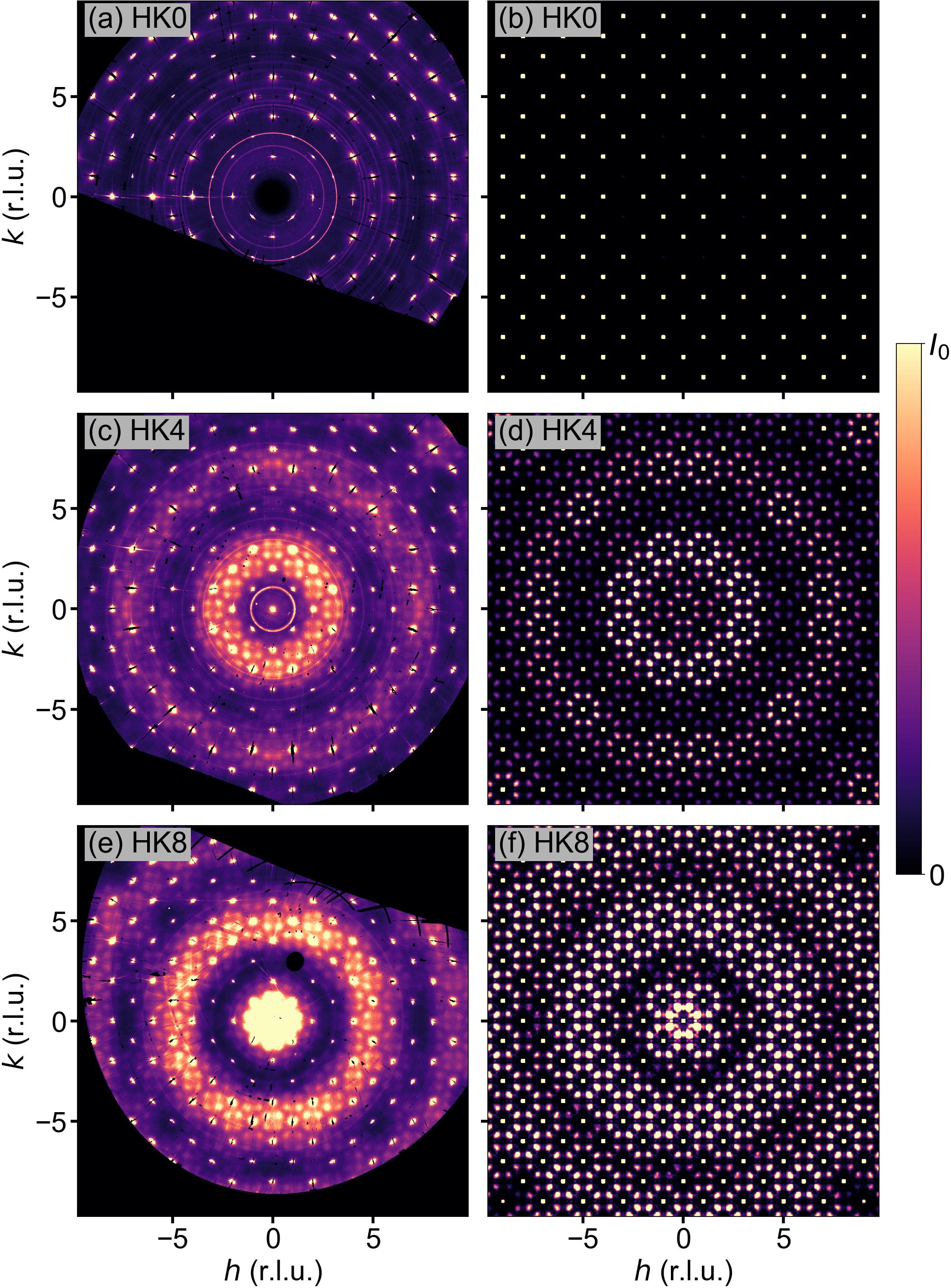
In Section III.1, we claim the possibility of local disorder above CDW contributing to the elusive (TaSe4)2I transport behavior. Here we report the observation of diffuse satellites far weaker than the CDW satellites which persist both above and below CDW, revealed by our high signal-to-noise synchrotron data. Figure 9 shows eight diffuse peaks surrounding each Bragg reflection in an octagon-like formation, and are confined within HK planes every four reciprocal lattice units along the L direction. We will refer to these as octagon satellites due to their positioning. Collectively, the octagon satellites form bright, concentric rings which alternate in pattern between each HK plane. The peaks are absent at the HK0 plane, but increase with intensity as L increases.
The methodology we used for simulating the CDW peaks can help elucidate the potential real-space source of the octagon peaks. Considering there are eight peaks around each Bragg reflection, we start again by applying four separate modulation waves to a (TaSe4)2I unit cell lattice, with each modulation assigned to its own equally sized domain. The wavevectors are set in one of four directions from and , which describe the positions of the vertices of an octagon centered on the origin.
Transverse displacement waves with amplitudes of 0.13 Å were used in our successful simulations. All atoms were set to oscillate along the direction, and the wavelength was calculated and chosen to align and overlap neighboring Bragg position satellites. Figure 9 shows the results of this simulation. Our model captures the rings of intensity collectively created by the intensity distribution of the octagon satellites. The rings alternate in position along the direction. Cross sections of the rings are visible as intense, segmented lines oriented along the H or K directions like those seen in Fig. 11. Additionally, the model correctly avoids simulating satellites at the HK0 plane. The intensity scaling among all the plots in Fig. 9 remains consistent, showing that the intensity of the octagon satellites increases as we move further from the HK0 plane along the L direction. Remarkably, modulation of the iodine positions is not necessary to obtain the experimental patterns. Any combination of modulations on the three atom types gave the correct satellite positions, but we found that modulating only the Se and Ta atoms together was needed to mimic the intensity distributions. Including the iodine ion gave redundant results, and any other modulation combination failed to simulate the distinct bright rings collectively created by the experimental satellites (Supplemental Material sup , Fig. S5).
We also considered density waves applied to all atoms with removal probabilities ranging between 0 and . The results of this simulation are shown in Fig. S6 of the Supplemental Material sup . Calculations from density waves create the correct first-order satellites, but they incorrectly simulate satellite peaks in the HK0 plane which do not increase in intensity along the L direction as seen in the experimental scattering. Transverse displacement waves capture experimental trends more closely because the satellites feature an increase with intensity along the direction of the oscillations, starting from zero intensity and proceeding to infinity as distance from the wave’s axis of propagation increases.
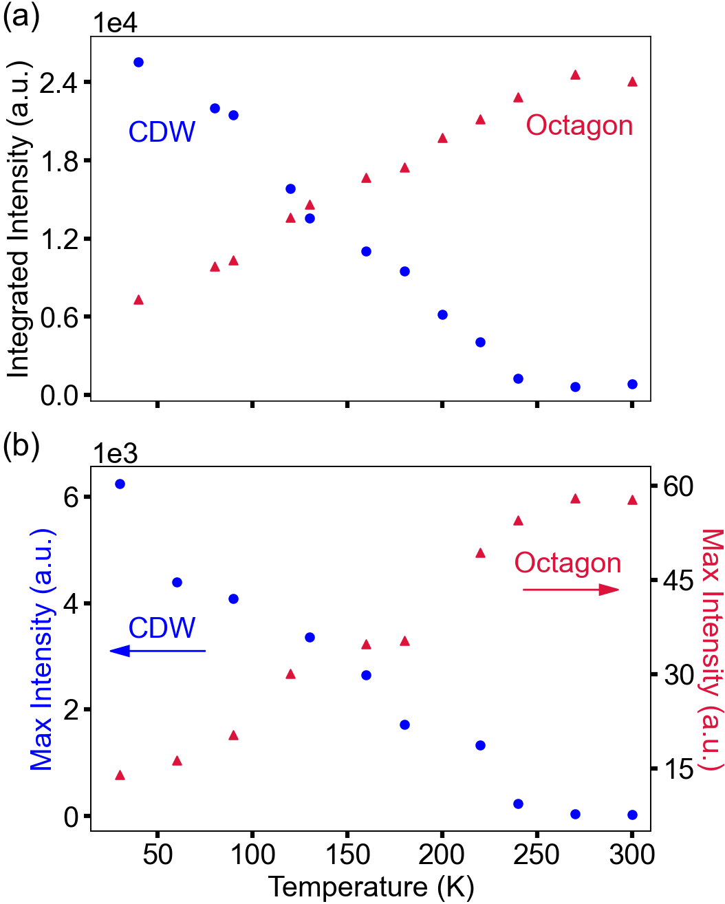
A comparison of intensities with respect to temperature between the octagon and CDW peaks can be found in Fig. 10. Make note that the octagon and CDW integrated intensities are of similar scale, but the maximum intensities differ by a couple orders of magnitude. We notice that the octagon peaks increase in intensity with temperature, and persist above the transition temperature where the CDW peaks do not. Additionally, the octagon peaks tend to subtly shift position within the HK plane and become more diffuse as temperature increases (see Fig. S7 in the Supplemental Material sup ). These features alone may suggest that the octagon peaks originate from dynamical (phonon) modulations or electronic coupling to them (polarons).Tournier-Colletta et al. (2013); Perfetti et al. (2001); Sinchenko et al. (2022) We also notice, however, that the intensities of the peaks level off above the CDW transition temperature. Perhaps the short-range, disordered modulations of the octagon peaks compete with the CDW phase modulations, an explanation for the comparable strength and inverse relationship between the integrated intensities. Further spectroscopic and high-temperature investigation is required.
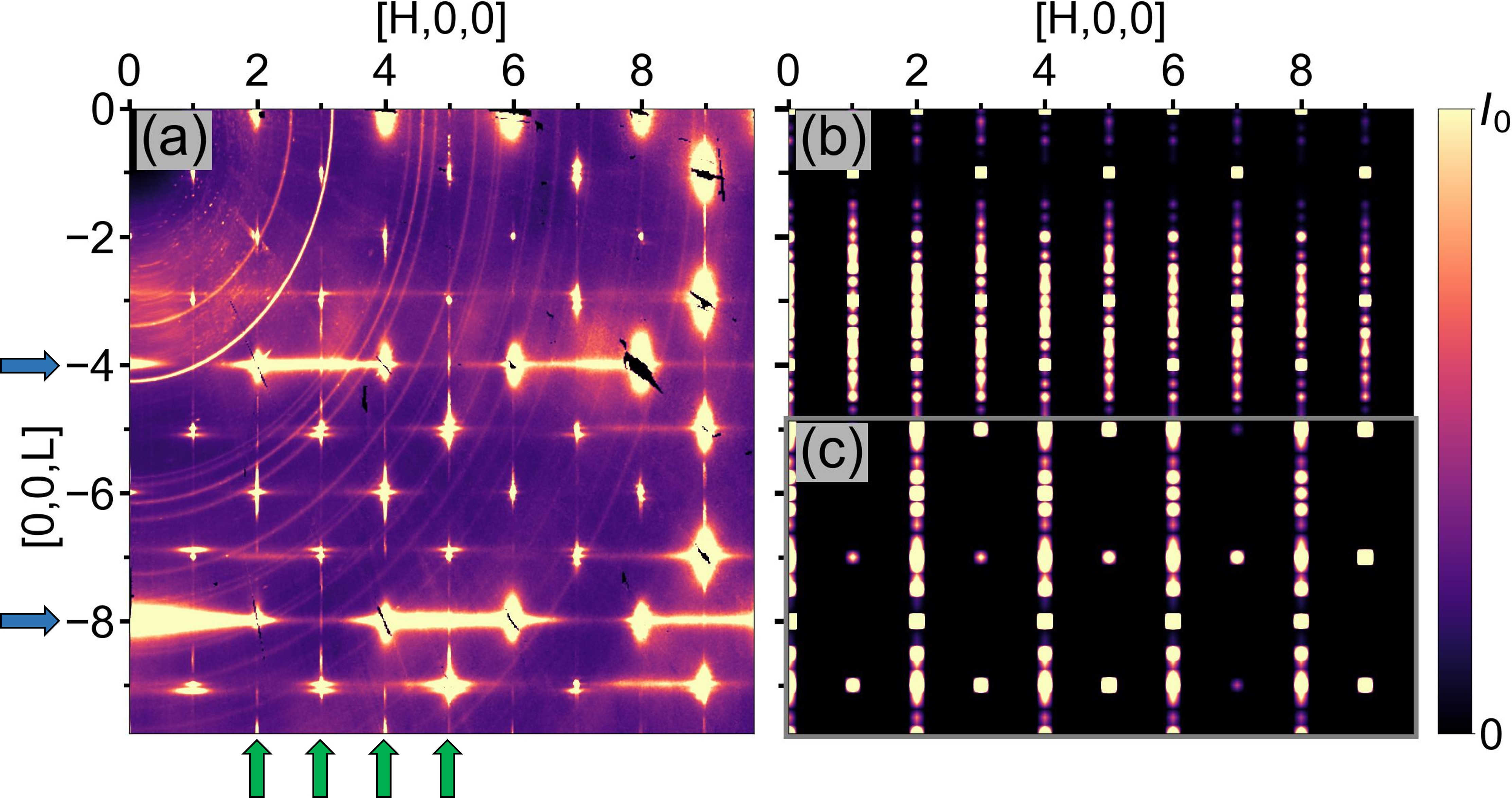
A separate feature from the displacement-driven octagon modulation is diffuse rods found running along the L direction, repeating every integer in reciprocal lattice units as demonstrated in Fig. 11(a). These diffuse features are present at all temperatures measured, from 30 K to 300 K. We can recreate similar behavior by removing or shifting entire planes of atoms along the direction (Fig. 7(d)). The entire plane must be shifted in order to preserve the ordering in directions perpendicular to the shift. This ensures we only simulate diffuse scattering along a single direction. When only iodine are removed and adjusted, diffuse rods appear in the simulated pattern every integer along H as seen in Fig. 11(b). The simulated diffraction patterns show a stronger intensity of diffuse rods along L than the experimental data, but these simulated rods are still qualitatively similar to the rods marked by the green arrows in the experimental scattering. On the other hand, when tantalum or selenium planes are removed and shifted, diffuse rods are created at every other integer value as seen in Fig. 11(c), so only half of the rods marked with green arrows are accounted for. For this simulation approach, iodine deficiency, and not Ta or Se, leads to the formation of rods at every integer H. The iodine ions are shifted into the highest occupancy positions, the I1A sites found halfway between the regular positions as seen in our refined unit cell (Fig. 3(b)). We modeled our simulation in this manner so that it resembles behavior suggested by the iodine occupancies of our crystal refinements. Missing iodine ions cause a relaxation of neighboring atoms towards the gaps, akin to a charge density wave. Unlike the regular, long-range ordering of the CDW phase modulations, the diffuse rods point to a highly disordered shift with short range ordering. Planes to remove and shift are chosen randomly in our simulation, but with a probability that ensures an iodine deficiency of about 10%, matching the single-crystal XRD refined values.
IV Conclusions
We have demonstrated the chirality trends of the one-dimensional Weyl semimetal (TaSe4)2I through single-crystal XRD refinements, ADF-STEM imaging, and helicity-dependent photocurrents. Based on XRD refinement parameters, each separately formed (TaSe4)2I crystal is likely to be enantiopure, while handedness may vary from crystal to crystal within the same synthesis batch conditions. The formation of chiral domain boundaries in (TaSe4)2I crystals grown by vapor transport is likely rare, and chirality-dependent transport and optical measurements of these materials can likely assume enantiopurity if a preliminary screening is performed via measurement of Flack parameters.
The single-crystal XRD refinements also revealed a bulk iodine deficiency in our (TaSe4)2I crystals. An average iodine fractional occupancy of 0.88(2) was observed. In general, a bulk iodine deficiency will profoundly impact the band structure of (TaSe4)2I. Defect formation and the subsequent relaxation of the (TaSe4)2I structure can lead to localized electrons, contributing to the semiconductor/insulator resistivity behavior observed in (TaSe4)2I in its high temperature phase, above the formation of a long-range CDW. As a possible footprint of this effect, diffuse scattering streaks can be modeled with concerted motion and disorder of iodine ions along the direction.
Our real-space pictures of diffuse scattering gives credence to previously hypothesized models for the (TaSe4)2I low temperature phase. The stronger modulation of the CDW phase was simulated using four separate, equal-sized domains, each with their own equivalent transverse displacement wavevector as described by Van Smaalen, et al Smaalen et al. (2001). Lower-intensity satellites confined to planes orthogonal to the direction were also observed with high signal-to-noise synchrotron data. We modeled these satellites with additional transverse displacement wavevectors, only requiring modulation of the tantalum and selenium atomic positions. Whether these satellites are the result of dynamical or static modulations is unknown at this point. The positive correlation of intensity with temperature and persistence beyond the CDW phase transition suggests these lower-intensity satellites are the result of dynamical modulations. On the other hand, the intensity trend appears to level off beyond the CDW temperature, and an inverse relationship with the CDW satellite integrated intensities would instead suggest static modulations which compete with the CDW modulations. The results of this study paint a clearer picture of the (TaSe4)2I structure at both low and high temperatures, and open the way for additional real-space studies.
Acknowledgements.
Sample synthesis, X-ray and THz analysis, and modeling were supported by the Center for Quantum Sensing and Quantum Materials, an Energy Frontier Research Center funded by the U.S. Department of Energy (DOE), Office of Science, Basic Energy Sciences (BES), under Award DE-SC002123. Synchrotron studies were performed at the Advanced Photon Source, a U.S. DOE Office of Science user facility operated for the DOE Office of Science by Argonne National Laboratory under Contract No. DE-AC02-06CH11357. Diffuse scattering modeling was performed on the High Throughput Computing Cluster of the Illinois Campus Cluster, a computing resource that is operated by the Illinois Campus Cluster Program (ICCP) in conjunction with the National Center for Supercomputing Applications (NCSA) and which is supported by funds from the University of Illinois at Urbana-Champaign. Laboratory X-ray and STEM characterization was carried out in part in the Materials Research Laboratory Central Research Facilities, University of Illinois. The STEM experiments were supported by the Air Force Office of Scientific Research under Award FA9550-20-1-0302 and by the National Science Foundation under Grant No. 1922758. We acknowledge additional support from the EPiQS program of the Gordon and Betty Moore Foundation (Grant GBMF11069 for Y.L. and F.M. and Grant GBMF4305 for P.A.). S.B. acknowledges support through the Early Postdoc.Mobility program from the Swiss National Science Foundation (Grant P2EZP2 191885).References
- Wieder et al. (2022) B. J. Wieder, B. Bradlyn, J. Cano, Z. Wang, M. G. Vergniory, L. Elcoro, A. A. Soluyanov, C. Felser, T. Neupert, N. Regnault, and B. A. Bernevig, Nature Reviews Materials 7, 196 (2022).
- Fu et al. (2007) L. Fu, C. L. Kane, and E. J. Mele, Physical Review Letters 98, 106803 (2007).
- Moore and Balents (2007) J. E. Moore and L. Balents, Physical Review B 75, 121306(R) (2007).
- Qi and Zhang (2011) X.-L. Qi and S.-C. Zhang, Reviews of Modern Physics 83, 1057 (2011).
- Kumar et al. (2021) N. Kumar, S. N. Guin, K. Manna, C. Shekhar, and C. Felser, Chemical Reviews 121, 2780 (2021).
- Hasan and Kane (2010) M. Z. Hasan and C. L. Kane, Reviews of Modern Physics 82, 3045 (2010).
- Moore (2010) J. E. Moore, Nature 464, 194 (2010).
- B. A. Bernevig and Hughes (2013) B. A. Bernevig and T. L. Hughes, Topological Insulators and Topological Superconductors (Princeton University Press, 2013).
- Wan et al. (2011) X. Wan, A. M. Turner, A. Vishwanath, and S. Y. Savrasov, Physical Review B 83, 205101 (2011).
- Yan and Felser (2017) B. Yan and C. Felser, Annual Review of Condensed Matter Physics 8, 337 (2017).
- Narang et al. (2021) P. Narang, C. A. C. Garcia, and C. Felser, Nature Materials 20, 293 (2021).
- Shi et al. (2021) W. Shi, B. J. Wieder, H. L. Meyerheim, Y. Sun, Y. Zhang, Y. Li, L. Shen, Y. Qi, L. Yang, J. Jena, P. Werner, K. Koepernik, S. Parkin, Y. Chen, C. Felser, B. A. Bernevig, and Z. Wang, Nature Physics 17, 381 (2021).
- Weyl (1929) H. Weyl, Zeitschrift für Physik 56, 330 (1929).
- Potter et al. (2014) A. C. Potter, I. Kimchi, and A. Vishwanath, Nature Communications 5, 5161 (2014).
- Xu et al. (2015) S.-Y. Xu, I. Belopolski, N. Alidoust, M. Neupane, G. Bian, C. Zhang, R. Sankar, G. Chang, Z. Yuan, C.-C. Lee, S.-M. Huang, H. Zheng, J. Ma, D. S. Sanchez, B. Wang, A. Bansil, F. Chou, P. P. Shibayev, H. Lin, S. Jia, and M. Z. Hasan, Science 349, 613 (2015).
- Jia et al. (2016) S. Jia, S.-Y. Xu, and M. Z. Hasan, Nature Materials 15, 1140 (2016).
- Hasan et al. (2017) M. Z. Hasan, S.-Y. Xu, I. Belopolski, and S.-M. Huang, Annual Review of Condensed Matter Physics 8, 289 (2017).
- Castro Neto et al. (2009) A. H. Castro Neto, F. Guinea, N. M. R. Peres, K. S. Novoselov, and A. K. Geim, Reviews of Modern Physics 81, 109 (2009).
- Weng et al. (2015) H. Weng, C. Fang, Z. Fang, B. A. Bernevig, and X. Dai, Physical Review X 5, 011029 (2015).
- Liu and Vanderbilt (2014) J. Liu and D. Vanderbilt, Physical Review B 90, 155316 (2014).
- Gressier et al. (1982) P. Gressier, L. Guemas, and A. Meerschaut, Acta Crystallographica Section B: Structural Crystallography and Crystal Chemistry 38, 2877 (1982).
- Gressier et al. (1984) P. Gressier, M. H. Whangbo, A. Meerschaut, and J. Rouxel, Inorganic Chemistry 23, 1221 (1984).
- Zhong et al. (2016) S. Zhong, J. E. Moore, and I. Souza, Physical Review Letters 116, 077201 (2016).
- Sanchez et al. (2019) D. S. Sanchez, I. Belopolski, T. A. Cochran, X. Xu, J.-X. Yin, G. Chang, W. Xie, K. Manna, V. Süß, C.-Y. Huang, N. Alidoust, D. Multer, S. S. Zhang, N. Shumiya, X. Wang, G.-Q. Wang, T.-R. Chang, C. Felser, S.-Y. Xu, S. Jia, H. Lin, and M. Z. Hasan, Nature 567, 500 (2019).
- Schröter et al. (2019) N. B. M. Schröter, D. Pei, M. G. Vergniory, Y. Sun, K. Manna, F. de Juan, J. A. Krieger, V. Süss, M. Schmidt, P. Dudin, B. Bradlyn, T. K. Kim, T. Schmitt, C. Cacho, C. Felser, V. N. Strocov, and Y. Chen, Nature Physics 15, 759 (2019).
- Asnin et al. (1979) V. M. Asnin, A. A. Bakun, A. M. Danishevskii, E. L. Ivchenko, G. E. Pikus, and A. A. Rogachev, Solid State Communications 30, 565 (1979).
- Belinicher and Sturman (1980) V. I. Belinicher and B. I. Sturman, Soviet Physics Uspekhi 23, 199 (1980).
- de Juan et al. (2017) F. de Juan, A. G. Grushin, T. Morimoto, and J. E. Moore, Nature Communications 8, 15995 (2017).
- Rees et al. (2020) D. Rees, K. Manna, B. Lu, T. Morimoto, H. Borrmann, C. Felser, J. E. Moore, D. H. Torchinsky, and J. Orenstein, Science Advances 6, eaba0509 (2020).
- Maki et al. (1983) M. Maki, M. Kaiser, A. Zettl, and G. Grüner, Solid State Communications 46, 497 (1983).
- Wang et al. (1983) Z. Z. Wang, M. C. Saint-Lager, P. Monceau, M. Renard, P. Gressier, A. Meerschaut, L. Guemas, and J. Rouxel, Solid State Communications 46, 325 (1983).
- Wang and Zhang (2013) Z. Wang and S.-C. Zhang, Physical Review B 87, 161107 (2013).
- Sekine and Nomura (2021) A. Sekine and K. Nomura, Journal of Applied Physics 129, 141101 (2021).
- Gooth et al. (2019) J. Gooth, B. Bradlyn, S. Honnali, C. Schindler, N. Kumar, J. Noky, Y. Qi, C. Shekhar, Y. Sun, Z. Wang, B. A. Bernevig, and C. Felser, Nature 575, 315 (2019).
- Sinchenko et al. (2022) A. A. Sinchenko, R. Ballou, J. E. Lorenzo, T. Grenet, and P. Monceau, Applied Physics Letters 120, 063102 (2022).
- Grüner (2019) G. Grüner, Density waves in solids (CRC Press, 2019).
- Voit et al. (2000) J. Voit, L. Perfetti, F. Zwick, H. Berger, G. Margaritondo, G. Grüner, H. Höchst, and M. Grioni, Science 290, 501 (2000).
- Monceau (2012) P. Monceau, Advances in Physics 61, 325 (2012).
- Tournier-Colletta et al. (2013) C. Tournier-Colletta, L. Moreschini, G. Autès, S. Moser, A. Crepaldi, H. Berger, A. L. Walter, K. S. Kim, A. Bostwick, P. Monceau, E. Rotenberg, O. V. Yazyev, and M. Grioni, Physical Review Letters 110, 236401 (2013).
- Zhang et al. (2020) Y. Zhang, L.-F. Lin, A. Moreo, S. Dong, and E. Dagotto, Physical Review B 101, 174106 (2020).
- Lee et al. (1985) K. B. Lee, D. Davidov, and A. J. Heeger, Solid State Communications 54, 673 (1985).
- Lorenzo et al. (1998) J. E. Lorenzo, R. Currat, P. Monceau, B. Hennion, H. Berger, and F. Levy, Journal of Physics: Condensed Matter 10, 5039 (1998).
- Smaalen et al. (2001) S. v. Smaalen, E. J. Lam, and J. Lüdecke, Journal of Physics: Condensed Matter 13, 9923 (2001).
- Favre-Nicolin et al. (2001) V. Favre-Nicolin, S. Bos, J. E. Lorenzo, J.-L. Hodeau, J.-F. Berar, P. Monceau, R. Currat, F. Levy, and H. Berger, Physical Review Letters 87, 015502 (2001).
- (45) See Supplemental Material at [URL will be inserted by publisher] for lattice modeling details, powder XRD refinements, single-crystal XRD refinement parameters, mircographs for TEM, satellite peak profiles, and additional diffuse scattering simulations.
- Krogstad et al. (2020) M. J. Krogstad, S. Rosenkranz, J. M. Wozniak, G. Jennings, J. P. C. Ruff, J. T. Vaughey, and R. Osborn, Nature Materials 19, 63 (2020).
- Jennings (2016) G. Jennings, “Cctw crystal coordinate transformation workflow,” (2016).
- Sheldrick (2015) G. M. Sheldrick, Acta Crystallographica Section C 71, 3 (2015).
- Proffen and Neder (1997) T. Proffen and R. B. Neder, Journal of Applied Crystallography 30, 171 (1997).
- Proffen and Neder (1999) T. Proffen and R. B. Neder, Journal of Applied Crystallography 32, 838 (1999).
- Neder and Proffen (2008) R. B. Neder and T. Proffen, Diffuse scattering and defect structure simulations: A cook book using the program discus (International Union of Crystallography, 2008).
- Forró et al. (1987) L. Forró, J. R. Cooper, A. Jánossy, and M. Maki, Solid State Communications 62, 715 (1987).
- Kim et al. (2021) S. Kim, R. C. McKay, N. Bielinski, C. Zhao, M.-K. Lin, J. A. Hlevyack, X. Guo, S.-K. Mo, P. Abbamonte, T.-C. Chiang, A. Schleife, D. P. Shoemaker, B. Bradlyn, and F. Mahmood, (2021), arXiv:2108.10874 [cond-mat.str-el] .
- Crepaldi et al. (2022) A. Crepaldi, M. Puppin, D. Gosálbez-Martínez, L. Moreschini, F. Cilento, H. Berger, O. V. Yazyev, M. Chergui, and M. Grioni, Journal of Physics: Materials 5, 044006 (2022).
- Perfetti et al. (2001) L. Perfetti, H. Berger, A. Reginelli, L. Degiorgi, H. Höchst, J. Voit, G. Margaritondo, and M. Grioni, Physical Review Letters 87, 216404 (2001).
- Flack (1983) H. D. Flack, Acta Crystallographica Section A: Foundations of Crystallography 39, 876 (1983).
- Flack and Bernardinelli (2008) H. D. Flack and G. Bernardinelli, Chirality 20, 681 (2008).
- Parsons et al. (2013) S. Parsons, H. D. Flack, and T. Wagner, Acta Crystallographica Section B: Structural Science, Crystal Engineering and Materials 69, 249 (2013).
- Watkin and Cooper (2020) D. J. Watkin and R. I. Cooper, Chemistry 2, 796 (2020).
- Valentín-Pérez et al. (2022) A. Valentín-Pérez, P. Rosa, E. A. Hillard, and M. Giorgi, Chirality 34, 163 (2022).
- Yi et al. (2021) H. Yi, Z. Huang, W. Shi, L. Min, R. Wu, C. M. Polley, R. Zhang, Y.-F. Zhao, L.-J. Zhou, J. Adell, X. Gui, W. Xie, M. H. W. Chan, Z. Mao, Z. Wang, W. Wu, and C.-Z. Chang, Physical Review Research 3, 013271 (2021).
- di Gregorio et al. (2020) M. C. di Gregorio, L. J. W. Shimon, V. Brumfeld, L. Houben, M. Lahav, and M. E. van der Boom, Nature Communications 11, 380 (2020).
- Dong and Ma (2020) Z. Dong and Y. Ma, Nature Communications 11, 1588 (2020).
- Sturman and Fridkin (1992) B. I. Sturman and V. M. Fridkin, The Photovoltaic and Photorefractive Effects in Noncentrosymmetric Materials (Gordon and Breach Science Publishers, New York, 1992).
- Chang et al. (2018) G. Chang, B. J. Wieder, F. Schindler, D. S. Sanchez, I. Belopolski, S.-M. Huang, B. Singh, D. Wu, T.-R. Chang, T. Neupert, S.-Y. Xu, H. Lin, and M. Z. Hasan, Nature Materials 17, 978 (2018).
- Fujishita et al. (1985) H. Fujishita, M. Sato, and S. Hoshino, Journal of Physics C: Solid State Physics 18, 1105 (1985).
- Fujishita et al. (1984) H. Fujishita, M. Sato, and S. Hoshino, Solid State Communications 49, 313 (1984).
- Fujishita et al. (1986) H. Fujishita, S. M. Shapiro, M. Sato, and S. Hoshino, Journal of Physics C: Solid State Physics 19, 3049 (1986).
- Nguyen et al. (2022) Q. L. Nguyen, R. A. Duncan, G. Orenstein, Y. Huang, V. Krapivin, G. de la Pena, C. Ornelas-Skarin, D. A. Reis, P. Abbamonte, S. Bettler, M. Chollet, M. C. Hoffmann, M. Hurley, S. Kim, P. S. Kirchmann, Y. Kubota, F. Mahmood, A. Miller, T. Osaka, K. Qu, T. Sato, D. P. Shoemaker, N. Sirica, S. Song, J. Stanton, S. W. Teitelbaum, S. E. Tilton, T. Togashi, D. Zhu, and M. Trigo, (2022), 10.48550/arXiv.2210.17483.
- Monceau et al. (1986) P. Monceau, L. Bernard, R. Currat, F. Levy, and J. Rouxel, Physica B+C Neutron Scattering, 136, 352 (1986).