fiFIfault injection \newabbreviationicICintegrated circuit \newabbreviationasicASICapplication-specific integrated circuit \newabbreviationtrcTRCtime replica circuit \newabbreviationtdcTDCtime-to-digital converter \newabbreviationmfiMFImultiple fault injection \newabbreviationpchPCHPlatform Controller Hub \newabbreviationcsmeCSMEConverged Security and Management Engine \newabbreviationfpgaFPGAfield-programmable gate array \newabbreviationdutDuTdevice under test \newabbreviationcfiCFIclock fault injection \newabbreviationvfiVFIvoltage fault injection \newabbreviationemEMelectromagnetic \newabbreviationemfiEMFIelectromagnetic FI \newabbreviationlfiLFIlaser fault injection \newabbreviationbbiBBIbody-biasing injection \newabbreviationisaISAinstruction set architecture \newabbreviationriscRISCreduced instruction set computer \newabbreviationporPoRpower-on-reset \newabbreviationslbSLBsoftware level-based \newabbreviationhlbHLBhardware level-based \newabbreviationpemPEMphoton emission microscopy \newabbreviationeofmEOFMelectro-optical frequency mapping \newabbreviationeopEOPelectro-optical probing \newabbreviationlitLITlock-in thermography \newabbreviationfaFAfailure analysis \newabbreviationirIRinfrared \newabbreviationnirNIRnear-infrared \newabbreviationsemSEMscanning electron microscope \newabbreviationllsiLLSIlaser logic state imaging \newabbreviationsocSoCsystem-on-chip \newabbreviationlsmLSMlaser scanning microscope \newabbreviationpdnPDNpower delivery network \newabbreviationpcbPCBprinted circuit board \newabbreviationscaSCAside-channel analysis \newabbreviationpufPUFphysical unclonable function \newabbreviationemscEMSCelectromagnetic side channel \newabbreviationcpuCPUcentral processing unit \newabbreviationichICHI/O Controller Hub \newabbreviationnaNAnumerical aperture \newabbreviationmcuMCUmicro-controller unit \newabbreviationffFFflip-flop \newabbreviationpsuPSUpower supply unit
Modulation to the Rescue: Identifying Sub-Circuitry in the Transistor Morass for Targeted Analysis
Abstract.
Physical attacks form one of the most severe threats against secure computing platforms. Their criticality arises from their corresponding threat model: By, e.g., passively measuring an ’s environment during a security-related operation, internal secrets may be disclosed. Furthermore, by actively disturbing the physical runtime environment of an , an adversary can cause a specific, exploitable misbehavior. The set of physical attacks consists of techniques that apply either globally or locally. When compared to global techniques, local techniques exhibit a much higher precision, hence having the potential to be used in advanced attack scenarios. However, using physical techniques with additional spatial dependency expands the parameter search space exponentially.
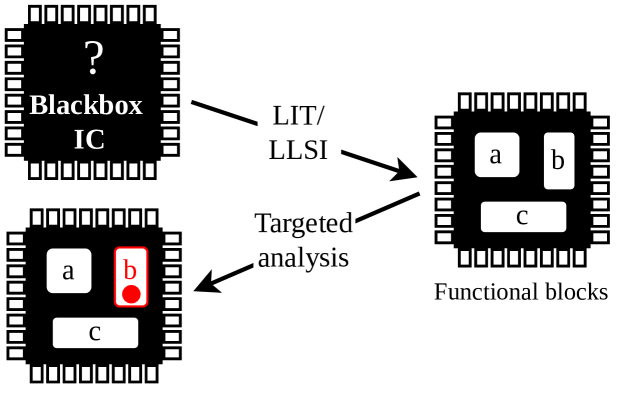
In this work, we present and compare two techniques, namely and , that can be used to discover sub-circuitry of an entirely unknown based on optical and thermal principles. We show that the time required to identify specific regions can be drastically reduced, thus lowering the complexity of physical attacks requiring positional information. Our case study on an Intel H610 Platform Controller Hub showcases that, depending on the targeted voltage rail, our technique reduces the search space by around to .
1. Introduction
Physical attacks, such as attacks or attacks, form one of the most severe threats against secure computing platforms. Their criticality lies within their corresponding threat model. By, e.g., passively measuring a processing unit’s environment during a security-critical operation, sensitive information may be leaked unintentionally, which leads to the disclosure of internal secrets (side-channel-power-analysis-of-an-aes-256-bootloader). Moreover, by actively disturbing the physical runtime environment of an , an adversary can deliberately cause specific misbehavior, which can be exploited afterward (oops-i-glitched-it-again). Hence, these powerful attacks can introduce vulnerabilities into systems where from a functional point of view, none exist.
A way to classify different physical attack scenarios is by their area of consideration. While global techniques (e.g., power analysis, voltage , or clock ) always consider the entire , local techniques affect or measure only a spatially restricted area. Local techniques, such as , , or analysis, make highly targeted attacks viable, as the considered region can be restricted to a specific target region. By exclusively covering a sub-region of interest of the , any side effects from and to surrounding components are avoided. Nonetheless, even for the class of localized techniques, there are differences to be considered: while , , and all provide means of spatial resolution, can be executed at a much finer granularity. In other words, the higher the spatial restriction is, the more precise an attack becomes. However, the gain in precision comes for the sake of complexity. As every additional parameter that has to be discovered during a physical attack increases the search space by exponential means (fill-your-boots; AMD_EM_fault), introducing locality in addition to the fault’s parameters (i.e., X-, Y-, and Z-position) results in a combinatorial explosion. If an adversary has to identify the target circuitry’s position on the entire silicon die, the resulting expansion of the search space leads to the impracticability of an otherwise feasible attack.
Due to the aforementioned expansion, a vast amount of research has been proposed to counter the expansion of search space under specific circumstances. breaking-black-box-crypto-devices-using-laser-fault-injection (breaking-black-box-crypto-devices-using-laser-fault-injection) proposed a method based on optical inspection to exclude specific regions of interest. In addition, they proposed the exploitation of side-channel information to further narrow the search space. By measuring the current while stimulating the ’s backside with a laser, On-the-complexity-reduction-of-laser-fault-injection-campaigns-using-OBIC-measurements (On-the-complexity-reduction-of-laser-fault-injection-campaigns-using-OBIC-measurements) showed for a given , that can be identified, which represent lucrative targets for in general. While previous work successfully identified areas of interest in specific circumstances, the general identification of regions on a black box silicon die still poses a hard task (AMD_EM_fault).
In this work, we propose the identification of sub-circuitry based on the modulation of specific, physically isolated voltage supplies. The modulation of a particular circuitry of interest via its voltage supply causes local physical effects, which can be measured by techniques commonly encountered in the domain. By modulating a single voltage rail while leaving the others unmodified, the external modulation manifests, e.g., in local temperature variation or a change in amplitude and phase of the reflected light when scanning over the chip with a laser.
Our contributions. We propose and as techniques for fast and targeted reverse engineering to simplify and speed up following analysis and attacks. As a case study, we evaluate our approach on a recent and highly complex technology, i.e., a manufactured by Intel along their 12th Gen. processor series. In this regard, we build a custom in order to be able to precisely control the individual power rails in an isolated manner. Based on our prototype, we show that the position of isolated functional blocks can be identified on the die. Finally, we compare and concerning their reverse engineering capabilities, resolution, and acquisition time.
2. Background
represents one of the last steps of the overall manufacturing process. After a wafer of has been manufactured by the semiconductor fabrication plant, the so-called yield determines the ratio of functional and non-functional . For a semiconductor product to be profitable and manufacturers to remain competitive, the yield must be maximized at all costs. However, the semiconductor manufacturing process of advanced is tremendously complex, i.e., not every part of the process can be controlled in its entirety. While this so-called process variation may be utilized positively to build intrinsic (physically-unclonable-functions), it also implies that a certain percentage of manufactured silicon malfunctions once the variation exceeds a given threshold.
is centered around localizing and characterizing a single ’s malfunctioning to tweak future production parameters, thus increasing the yield of future production runs. A variety of techniques exists, each exhibiting advantages and disadvantages in localizing or characterizing a specific kind of fault. In this work, we utilize two such methods, namely , which is based on thermal principles, and , which is based on laser scanning microscopy. In this section, both techniques are briefly introduced. Moreover, of modern are briefly discussed, as they are key to our approach.
2.1. Thermal Analysis of Integrated Circuits
In , is employed to localize thermally active regions, which indicate resistive defects in . Failure analysts use this method to, for example, localize resistive shorts between different metal lines, gate oxide breakdowns, and other faults that cause an increase in contact resistance. These resistive defects lead to higher power dissipation and, thus, to a local temperature increase. As the local temperature increase implies an increase in mid-range emanation (i.e., ), it can be captured by an -sensitive camera with high resolution. is based on capturing the thermal radiation in the mid-range spectrum emitted by an object.
Resistive defects usually cause power dissipation in the range, which translates to local temperature differences in the range. However, the sensitivity of high-end sensors lies in the range. Hence, to be able to measure the small temperature differences, lock-in amplification is mandatory. In , we inject a periodic signal into the , which is also fed into the lock-in amplifier as a reference. The lock-in amplifier then relates the thermal signal captured by the camera to the reference, filtering and amplifying the thermal information correlating to the induced modulation.
Moreover, it is worth noting that even a fully powered-off may exhibit a strong contrast in emissivity at room temperature due to the difference in emissivity of different materials and structures used in manufacturing. Hence, thermographic sensors can be used to record an ’s pattern through the backside.
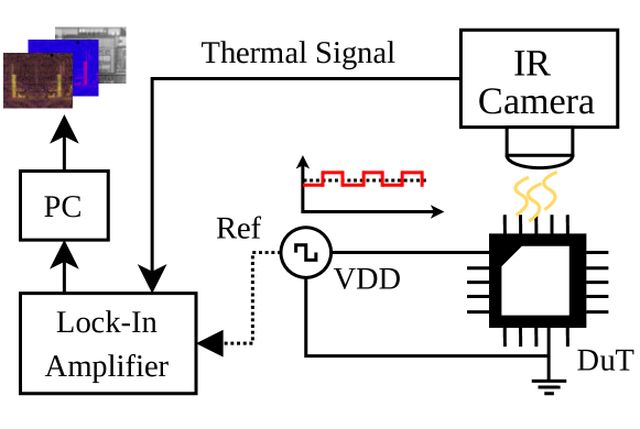
Figure 2 depicts a typical setup. In this work we exclusively consider complex exhibiting multiple voltage supplies as . Further, a high-resolution mid-range camera is required to capture temperature deviations based on a fine scale. Different lenses can be used to increase the spatial resolution of the camera. Every setup requires an external electrical stimulus fed into the . This is commonly achieved using a switchable that provides the external modulation in the form of a square wave of a given amplitude. The lock-in amplifier detects a low-amplitude thermal signal that correlates with the induced signal by performing integration over time. Finally, the PC receives temperature amplitude and phase information and stores the results for later analysis.
2.2. Laser-Based Analysis of Integrated Circuits
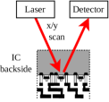
Modern are comprised of numerous metal layers on the chip’s front side, making any analysis through the front side impossible. Therefore, analysis is commonly executed through the chip’s backside. Since silicon is transparent to light, can be used to access the active area containing the transistors without preparing the silicon backside of the chip. One approach to localizing faults is stimulating the with a laser and measuring the change in resistance, voltage, or current consumption at the device’s terminals. On the other hand, some part of the laser irradiation is modulated by the electrical characteristics in the chip and reflected at metal interfaces, see Fig. 3a. Consequently, this reflected light contains information about the internal voltages of the chip. In , a detector captures the reflected light and translates its magnitude and phase into a corresponding signal. The approach is part of a family of methods, referred to as optical probing techniques. When pointing the laser at one location of interest, a waveform depicting voltage over time can be acquired. The corresponding technique is called . Besides, an activity map can be created when scanning the laser over a larger area of interest and analyzing the reflected light at each point. The technique is called , and due to its spatial capabilities, we will focus on in the following.
2.2.1. Electro-Optical Frequency Mapping
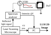
is an optical probing technique that allows the creation of a two-dimensional activity map of a circuit area. Provided a particular frequency and a bandwidth, analyzes the reflected light using a narrow-band frequency filter and maps the resulting amplitude onto the scanning position. In this way, all transistors switching at the frequency of interest appear as bright spots in the activity map. To not influence the electrical behavior of the , wavelengths above are used for optical probing techniques. Apart from debugging internal signals in , optical probing can be used to attack devices. For instance, in combination with has been used to extract sensitive data from a (tajik_power_2017) or to break logic locking schemes (rahman_key_2020).
2.2.2. Laser-Logic State Imaging
is an extension of proposed by niu_laser_2014 (niu_laser_2014). Instead of setting the frequency of to the frequency of a logic signal generated by the device, a periodic signal is injected into the ’s power supply, as depicted in Fig. 3b. In other words, the ’s power supply is modulated around the nominal supply voltage with a small peak-to-peak sine signal. is then used to search for activity based on the introduced modulation frequency. Using , the logic states of combinatorial and sequential logic can be extracted under the constraint that the clock is stopped for the duration of the measurement (krachenfel_realworld_2021; krachenfel_automatic_2021). Apart from transistor states, measurements reveal the location of capacitive elements, such as decoupling capacitors. Consequently, can be used to localize circuitry connected to the power supply rail under modulation.
2.3. Power Delivery Networks in Design
The of an