Also at ]HSE University
Laser-pump-resistive-probe technique to study nanosecond-scale relaxation processes
Abstract
Standard optical pump-probe techniques allow to study a temporal response of a system to a laser pulse starting from the sub-femtoseconds to several nanoseconds, limited by the length of the optical delay line. Resistance is a sensitive detector of a plethora of phenomena in solid state, nanostructure physics, chemistry, and biology. However, resistance measurements are typically rather slow (> microsecond) because they require stabilization of current or voltage and analog-to-digital conversion. Here we develop a time-resolved pump-probe technique, where the “Pump” is an optical pulse from the laser and the “Probe” is a rectangular electrical pulse passing through the sample under study. Transmission of the probe pulse through the sample is measured in the 50 Ohm matched circuit with the digital oscilloscope. The delay can be electrically driven from nanoseconds to seconds. We demonstrate the usability of the technique to study heat-induced changes in a thin amorphous VOx film and carrier relaxation in a CdS photoresistor. The technique could be further explored to study heat transfer, biochemical reactions, and slow electronic transformations.
I Introduction
The pump-probe technique is widely used to study the dynamics of various systems. The optical version of the scheme involves the use of two laser pulses: the first, called “Pump”, excites the system, and the second pulse, called “Probe”, measures the response of the system to the excitation after some time called delay. The temporal resolution of this method can reach hundreds of attoseconds Lara-Astiaso et al. (2018). On the upper side, the optical pump-probe is limited to a few nanoseconds by the length of the delay line (1 ns is equivalent to 30 cm). There are cases when the dynamics of an electronic system is longerSaǧol et al. (2002); He et al. (2021), e.g. relaxation of spin, heat, or macroscopic order parameters.
Conductivity reflects the immediate vicinity of the Fermi energy and might, thus, be sensitive to very subtle changes in temperature, deformation, energy spectrum, etc. However, its measurement process is slow due to current/voltage stabilization and processing. On the other hand, voltage pulse in an impedance-matched scheme can be measured much faster with an oscilloscope.
A technique combining an optic “Pump” and a pulsed electric “Probe” is straightforward. We develop a Pump-probe-like technique that would allow us to measure the relaxation of the arbitrary resistance, different from 50 Ohms, on a time scale from nanoseconds to seconds. Technically the realization is a bit tricky and for this reason, to the best of our knowledge, it was not demonstrated so far. It has something in common with the previous experimental efforts. For example, Stern et al.Stern et al. (2008) implemented a technique with an electrically pumped time-resolved Kerr rotation to study the dynamics of the spin Hall effect. To achieve 50 Ohm matching they adjusted carefully the sample’s geometry. An all-electrical pump-probe technique was demonstrated by Dirisaglik et al. Dirisaglik et al. (2015). They used various measurement waveforms to study a Ge2Sb2Te5 phase change memory device. Time-resolved carrier dynamics and conductivity measurements were also performed in Refs. Lutz et al., 1993; Zhitenev et al., 1993; Ramamoorthy et al., 2015; Vasile et al., 2006; Naser et al., 2005. They were 50 Ohm impedance matched and used pulse widths from a couple of nanoseconds to a few hundred nanoseconds.
A combination of optical excitation and time-resolved resistive measurements seems to be a powerful tool to explore new intermediate time-scale phenomena. We believe that this paper might stimulate the corresponding experiments.
II Method
II.1 Description of the experimental technique
The main idea of the laser-pump-resistive-probe method is simple. One needs 3 tools: a laser, a generator, and a digital oscilloscope. A laser system outputs a pump light pulse as well as an electrical sync pulse. The laser beam is focused on the sample with the help of mirrors and a microscope lens (if needed). The electrical sync pulse is used to trigger a generator. The generator outputs the probe pulse after an adjustable delay. Using an oscilloscope one can measure the voltage and calculate the resistance later. Such a simplified approach is shown in Fig. 1. Although the idea is simple, the practical realization is complicated due to impedance matching and unwanted time delays (e.g. generator input-to-output delay).
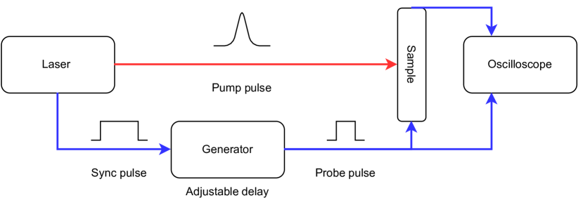
Using short-pulsed resistivity measurements instead of DC bias current and voltage readout is an important feature, that gives two major advantages. First, the delay time is practically unlimited. Oscilloscopes cannot record data with a high sample rate (several GSa/s) for several seconds due to memory limitations. Second, the pulse technique reduces the heating of the sample.
We use a Light Conversion PHAROS laser system with a wavelength of 1030 nm and a minimal pulse duration of 251 fs for “Pump” excitation. The laser system runs at a repetition rate of 25 kHz and is accompanied by a built-in pulse picker. The pulse picker allows to further reduce the frequency of laser pulses.
One of two options is used for probe pulse synthesis: (i) G5-78, a fast analog generator, that allows to achieve pulses with widths down to 1 ns; (ii) Tektronix AFG3152C, with a digitally controlled trigger to output delay (from hundreds ps to several seconds) and pulses with widths down to 5 ns. The measured jitter is around 50 ps for the G5-78 and around 75 ps for the Tektronix AFG3152C.
To collect the voltage data we use a Keysight DSO-S104A oscilloscope with 1 GHz bandwidth, a 10-bit analog-to-digital (ADC) converter, and up to 20 GSa/s acquisition rate in 2-channel mode or 10 GSa/s in 4-channel mode.
In the case of a Q-switched laser, the synchronization would be trivial: the laser is triggered from the generator. However, such lasers have limitations either in pulse duration (above several ns) or in pulse energy. For most ps and fs lasers, one requires synchronization with the internal timing module of the laser, which might be tricky, especially for delays close to zero. We provide details on synchronization in our setup in Appendix A
The equivalent electrical scheme of the measuring circuit is shown in Fig. 2. The pulse from the generator is divided: one part goes through the sample and the matching resistor to the 1st channel of the oscilloscope, and the other part goes to the 2nd channel of the oscilloscope. 50 Ohm coaxial cables are used for connections between the instruments and the sample.
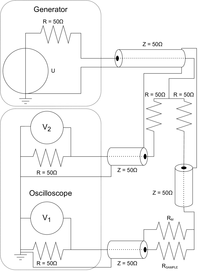
In a perfectly matched circuit the resistance of the sample should be expressed by the formula:
| (1) |
where is the sample resistance, is the resistance of the impedance matching resistor, and are the voltages on the 1st and 2nd channels of the oscilloscope, respectively. Note that sample resistance should not be too high, otherwise, will be immeasurably small. Low resistance (< 50 Ohm) samples have to be connected in series with a larger resistor to ensure 50 Ohm impedance matching.
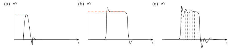
Probe pulses in the described setup can be as short as 1 ns. We demonstrate 1 ns pulse usage capabilities in Appendix B. However, due to unavoidable capacitive spikes in the beginning and at the end of rectangular pulses, such short widths can be used only when the circuit impedance is very close to 50 Ohm. In most cases, it is needed to increase the width of the probe pulse to 10 or more nanoseconds. Similar problems were described by the other researchers, see Vasile et al., 2006; Naser et al., 2005. Depending on the system under study (mostly on its capacity) one of three methods can be used to numerically determine and :
-
1.
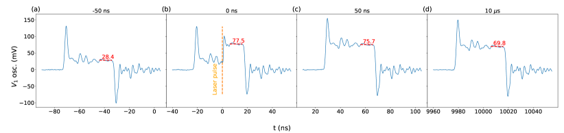
Maximum value on the oscillogram (for probe pulses shorter than 20 ns), schematically shown in Fig. 3(a).
-
2.
Mean value of the high level (for probe pulses longer than 20 ns or with short lead and trail), Fig. 3(b).
-
3.
Numerical integration of the signal part of the oscillogram (if the pulse shape is smeared by transient processes), Fig. 3(c).
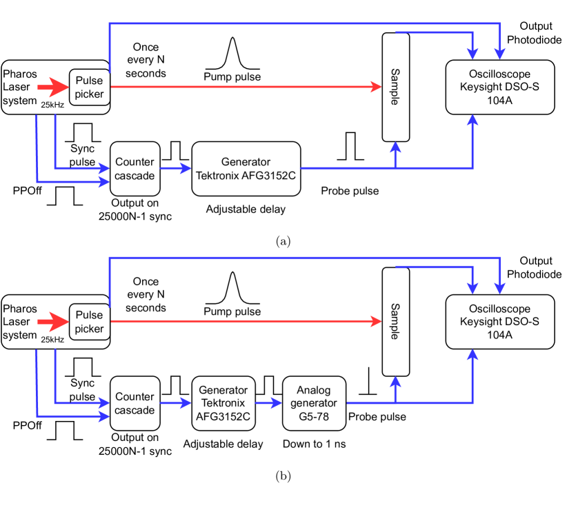
In case of slow measurements (pulse width >5 ns), the rectangular measurement pulse is generated by Tektronix AFG3152C directly, as shown in Fig. 4(a). In case of faster measurements, the generated pulse is used to trigger the analog generator. The combination of two generators allows both, fast probe pulses and digitally controlled delay, as shown in Fig. 4(b). The duration of the probe pulse is adjusted to be sufficient for the signal to reach a steady state. The closer the impedance of the measuring circuit to 50 Ohms, the shorter pulses can be used.
The data is collected over different delays using a Python script. Several oscillograms (usually 10-20) are acquired and averaged for each delay value.
III Samples
We demonstrate the usability of our setup on two types of photodective materials. The first one is a CdS-based photoresistor (GL5516, see datasheet: https://datasheetspdf.com/pdf-file/756925/SENBA/GL5516/1). CdS has a direct bandgap of 2.42 eV and long-standing photoconductivity caused by depopulation of impurity levels. The dark resistance of the film is too high. Therefore, it was additionally illuminated by an incandescent lamp with a constant luminosity of 95.1 0.3 lux. The luminosity was measured with a BH1750 sensor.
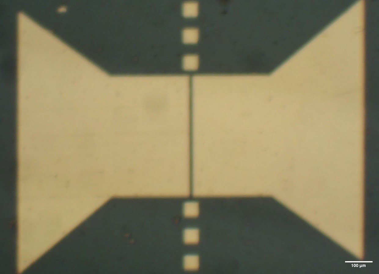
The second one is a thin amorphous VOx film. The film was deposited on a glass substrate in a Plassys MEB-550S. The deposition was carried out in a flow of oxygen (8 sccm) at room temperature at a rate of 0.1 nm/s. The thickness of the films was 50 nm. In fact, this film is a thermistor with a -2.56%/K temperature coefficient of resistivity in a wide range of temperatures (20-80 °C). Cr-Au contacts were lithographically defined and thermally evaporated using the lift-off method on top of the VOx film. The shape of the contacts is a short and wide bridge (450 m wide and 5 m long) so the resistance of the structure was suitable for the measurement range. A photo of the structure is presented in Fig. 5.
IV Results and discussion
IV.1 Dynamics of photoconductivity relaxation in CdS
For measurements of CdS photoconductivity relaxation probe pulse parameters were: 25 ns width, 7 V amplitude, 3 ns lead and trail. It is important to note that 7 V is the value of the generator output, not the voltage at the sample. Light pulses were kept once every two seconds. The matching resistor was 51 Ohm (RuO2 SMD). A barium borate (BBO) crystal was used to generate a second harmonic at 515 nm for the pump pulse.
Fig. 6 demonstrates oscillograms for different time delays: before the laser pulse (Fig. 6 (a)), at the laser pulse (Fig. 6(b)), and after the pulse (Fig. 6(c),(d)). One can see the transient processes happening in the circuit and the change in the voltage level, corresponding to the laser pulse. The resistance values are calculated using numerical integration. For this demonstration 40 ns width probe pulses were used.
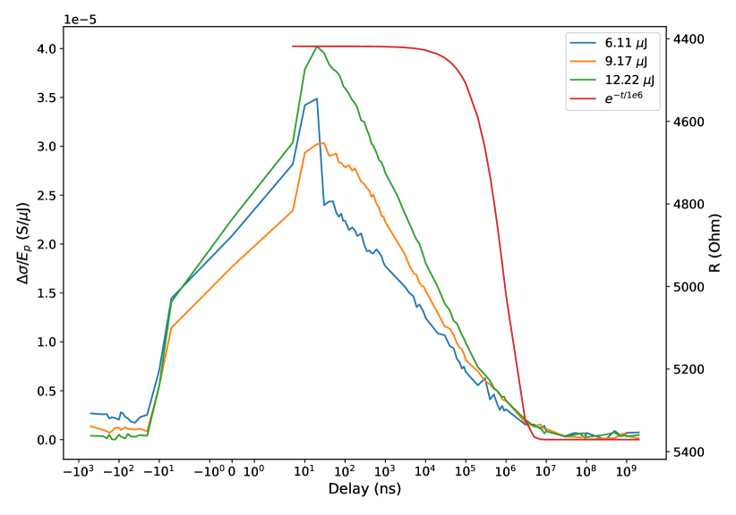
The relaxation curve for the photoconductivity, normalized by the energy of the pulse for three energy values is shown in Fig. 7. The X-axis scale of the relaxation curve is symmetric logarithmic.
Because the pulse part of the oscillogram was integrated, the resistance started to drop before the zero time point. At the time point of -12.5 ns the last part of the probe pulse starts to increase as in Fig. 6 (b) in the middle of the pulse.
CdS photoresistors are known to have about 100 millisecond photoconductivity relaxation time at room temperature. This is in contradiction with the experimental data, where relaxation begins at the sub-microsecond scale. This behavior could be explained by many charge trap model and two contributions (fast electrons and slow holes) in photoconductivityRyvkin (2012). In the region >100 s the normalized relaxation curves coincide. It means that the slowest traps in the band gap were not depopulated completely by the pump pulse. For lower delays, the curves differ strongly, which demonstrates the nonlinearity of light absorption. Alternatively, the sub-microsecond feature might come from overheating. Further studies are needed to clarify the sub-microsecond photoconductivity dynamics.
IV.2 Heat-induced processes
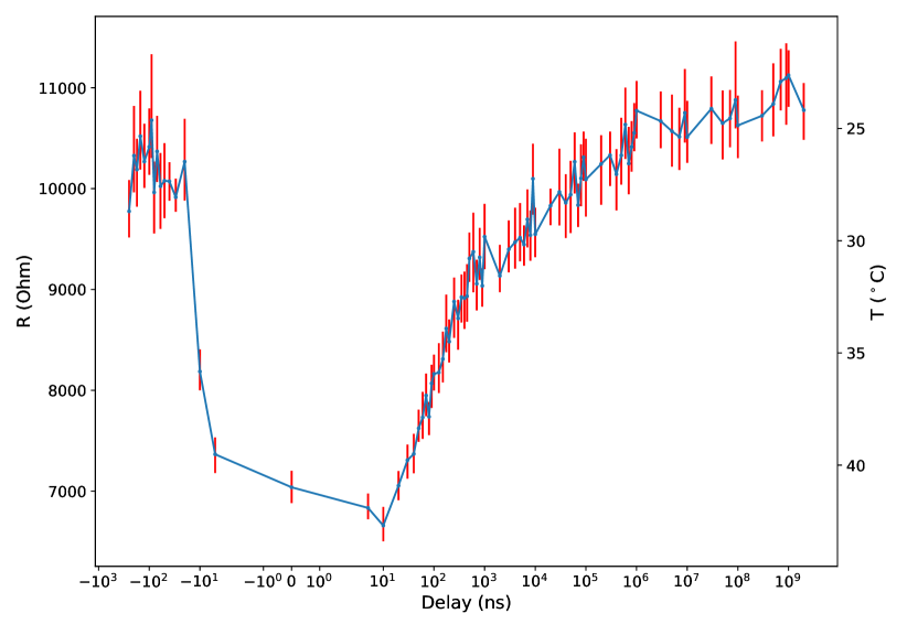
The relaxation curve for the VOx sample is shown in Fig. 8. In this case, the light pulse is used to heat a sample. Due to the geometry of the sample (see Fig. 5) and the low absorption of gold contacts and the substrate, the energy of one light pulse had to be high (110 microjoules) for registrable changes to occur. This led to the degradation of the film at the beginning of the experiment. After 5 minutes the sample was in a steady state and its resistance stopped drifting. The probe pulse parameters were 30 ns long, 7.5 V amplitude, 3 ns lead and trail. The matching resistor was a RuO2 SMD 51 Ohm resistor.
The X-axis scale of the relaxation curve shown in Fig. 8 is symmetric logarithmic. No exponential or power law relaxation is observed. One can see fast dynamics at low delays and slow dynamics at delays above 1 s. We think that fast dynamics at low delays originate from heat diffusion into gold contacts with high thermal conductivity. When gold contacts are thermalized, the heat flows into the substrate slowly.
Therefore, the proposed laser-pump-resistive-probe technique in combination with a thermosensitive resistor could serve as a tool for studying heat diffusion in bulk materials and microstructures.
V Conclusions
We developed a laser-pump-resistive-probe technique. The delay can be driven from nanoseconds to seconds. We describe the details of the method, demonstrate one nanosecond resolution and the usability of the proposed technique to study heat-induced changes and carrier relaxation.
The technique could be useful to study biochemical reactions, heat transfer, photoconductivity relaxation, and slow electronic transformations at a new timescale.
Acknowledgements.
The authors are thankful to E. V. Tarkaeva for her contribution to the sample fabrication and to A. Yu. Klokov for numerous thoughtful discussions. The work was supported by the Government of the Russian Federation (Contract No. 075-15-2021-598 at the P.N. Lebedev Physical Institute). VOx sample fabrication has been performed at the Shared research facility at the P.N. Lebedev Physical Institute.Appendix A Synchronization
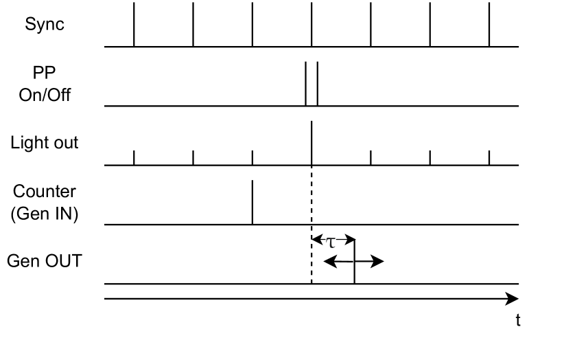
The most important pulse trains are schematically shown in Fig. 9 for better understanding. In our setup, the laser runs at 25 kHz but the built-in pulse picker is configured to pick a pulse only once every 2 seconds to allow the system to relax. The laser’s internal timing module outputs a synchronization pulse at a 25 kHz rate. Furthermore, the timing module outputs a Pulse Picker On (PPOn) signal every time a pulse picker picks a pulse (1 pulse per 50,000 sync pulses). The PPOn signal is emitted about a hundred ns before the light pulse and theoretically can be used to account for the extra time delays. Time delays mainly consist of input-to-output delay of digital generators. In our case, for Tektronix AFG3152C we measured a minimal input-to-output delay of about 300 ns. Thus, the PPOn pulse cannot be used for synchronization. If the pulse picker outputs a light pulse every two seconds, time points 0 ns and 2 s should be equivalent. However, at high delays, the generator has only a 100-microsecond resolution (5 digits), which is much higher than 1 ns and cannot be used for studying fast dynamics. Such input-to-output delays and limited resolutions are common for most digital generators.
To solve the problem, a homemade circuit to pretrigger the generator is used. It consists of 6 cascaded 74HC192 presettable counters and an SN74AC04DR inverter. This cascade outputs an electric pulse one synchronization pulse (40 s) before the light output. In our case, for a light pulse once every two seconds, the cascade will output on the 49999th synchronization pulse (because ). The Pulse Picker Off (PPOff) pulse, which is output by the laser’s timing module after the light pulse, is fed through the inverter to the parallel load pin of all counters to reset them to preloaded values. PPOff comes before the next synchronization pulse. The cycle repeats. The output of the cascade is used to trigger the generator. The Tektronix AFG3152C generator output pulse will match the light pulse arrival if the delay is set to about 40 microseconds (depending on the length of cables compared to the light path length). The 5-digit resolution of the generator is sufficient for adjusting the delay on the nanosecond scale. To ensure proper synchronization the third channel of the oscilloscope is used to record the PHAROS built-in output photodiode signal.
Appendix B Demonstration of nanosecond-wide pulses
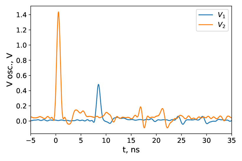
A demonstration setup with RuO2 resistors is used to show the possibility of the 1 ns pulse usage. Fig. 10 shows oscillograms from channels 1 and 2 (in orange and blue, respectively) of the oscilloscope. is 100.5 Ohm and is 100.3 Ohm. The formula 1 gives 115.4 Ohm. This is the best result. It was obtained using the peak value method for determining and . The amplitude of the probe pulse was 3.2V, lead and trail were 500 ps. The 15% disagreement shows that one should be very careful with nanosecond probe pulses and take into account all possible impedance mismatching.
References
- Lara-Astiaso et al. (2018) M. Lara-Astiaso, M. Galli, A. Trabattoni, A. Palacios, D. Ayuso, F. Frassetto, L. Poletto, S. D. Camillis, J. Greenwood, P. Decleva, I. Tavernelli, F. Calegari, M. Nisoli, and F. Martín, “Attosecond pump–probe spectroscopy of charge dynamics in tryptophan,” The Journal of Physical Chemistry Letters 9, 4570–4577 (2018).
- Saǧol et al. (2002) B. E. Saǧol, G. Nachtwei, K. von Klitzing, G. Hein, and K. Eberl, “Time scale of the excitation of electrons at the breakdown of the quantum hall effect,” Physical Review B 66 (2002), 10.1103/physrevb.66.075305.
- He et al. (2021) Y. He, B. Wang, L. Lüer, G. Feng, A. Osvet, T. Heumüller, C. Liu, W. Li, D. M. Guldi, N. Li, and C. J. Brabec, “Unraveling the charge-carrier dynamics from the femtosecond to the microsecond time scale in double-cable polymer-based single-component organic solar cells,” Advanced Energy Materials 12 (2021), 10.1002/aenm.202103406.
- Stern et al. (2008) N. P. Stern, D. W. Steuerman, S. Mack, A. C. Gossard, and D. D. Awschalom, “Time-resolved dynamics of the spin hall effect,” Nature Physics 4, 843–846 (2008).
- Dirisaglik et al. (2015) F. Dirisaglik, G. Bakan, Z. Jurado, S. Muneer, M. Akbulut, J. Rarey, L. Sullivan, M. Wennberg, A. King, L. Zhang, R. Nowak, C. Lam, H. Silva, and A. Gokirmak, “High speed, high temperature electrical characterization of phase change materials: Metastable phases, crystallization dynamics, and resistance drift,” Nanoscale 7, – (2015).
- Lutz et al. (1993) J. Lutz, F. Kuchar, K. Ismail, H. Nickel, and W. Schlapp, “Time resolved measurements of the energy relaxation in the 2deg of AlGaAs/GaAs,” Semiconductor Science and Technology 8, 399–402 (1993).
- Zhitenev et al. (1993) N. B. Zhitenev, R. J. Haug, K. v. Klitzing, and K. Eberl, “Time-resolved measurements of transport in edge channels,” Physical Review Letters 71, 2292–2295 (1993).
- Ramamoorthy et al. (2015) H. Ramamoorthy, R. Somphonsane, J. Radice, G. He, C.-P. Kwan, and J. P. Bird, ““freeing” graphene from its substrate: Observing intrinsic velocity saturation with rapid electrical pulsing,” Nano Letters 16, 399–403 (2015).
- Vasile et al. (2006) G. Vasile, C. Stellmach, G. Hein, and G. Nachtwei, “Measurements of the electrical excitation of quantum hall devices in the real-time domain,” Semiconductor Science and Technology 21, 1714–1719 (2006).
- Naser et al. (2005) B. Naser, J. Heeren, D. K. Ferry, and J. P. Bird, “50--matched system for low-temperature measurements of the time-resolved conductance of low-dimensional semiconductors,” Review of Scientific Instruments 76, 113905 (2005).
- Ryvkin (2012) S. M. Ryvkin, Photoelectric effects in semiconductors, 1964th ed. (Springer, New York, NY, 2012).