Spiking dynamics in dual free layer perpendicular magnetic tunnel junctions
Abstract
Spintronic devices have recently attracted a lot of attention in the field of unconventional computing due to their non-volatility for short and long term memory, non-linear fast response and relatively small footprint. Here we report how voltage driven magnetization dynamics of dual free layer perpendicular magnetic tunnel junctions enable to emulate spiking neurons in hardware. The output spiking rate was controlled by varying the dc bias voltage across the device. The field-free operation of this two-terminal device and its robustness against an externally applied magnetic field make it a suitable candidate to mimic neuron response in a dense Neural Network (NN). The small energy consumption of the device (4-16 pJ/spike) and its scalability are important benefits for embedded applications. This compact perpendicular magnetic tunnel junction structure could finally bring spiking neural networks (SNN) to sub-100nm size elements.
Spintec]Univ. Grenoble Alpes, CEA, CNRS, Grenoble-INP, SPINTEC, 38000 Grenoble, France Spintec]Univ. Grenoble Alpes, CEA, CNRS, Grenoble-INP, SPINTEC, 38000 Grenoble, France
Neuromorphic computing is a promising way to drastically reduce the energy consumption of artificial intelligence, by building systems that are inspired by the structure and function of the brain to process information more efficiently in hardware 1. While biological neurons emit voltage spikes, most software artificial neural networks are static and rate-based, meaning that the outputs of neurons encode a rate of spikes rather than spike themselves. However, spiking neural networks have several important advantages for further reducing energy consumption. The unitary nature of spikes enables spiking neural networks with sparse activity, as well as asynchronous and event-based communication 2. Furthermore, electrical spikes can modify the conductance state of nanodevice-based artificial synapses, making it possible to implement local learning rules, a critical ingredient for on-chip learning 3, 4. Spiking neurons have been implemented using several substrates: CMOS circuits 5, 6, 7, photonic devices 8 and memristive devices 9. However, spintronic spiking neurons are lacking. Spintronic-based neurons and synapses are a promising solution showing a significant reduction in energy consumption compared to CMOS-based circuits 10. Here we present an experimental demonstration of a spiking neuron implemented with a magnetic tunnel junction. Magnetic tunnel junctions combine the advantage of small size, high speed, low power consumption and CMOS compatibility. Our novel structure is based on a perpendicular magnetic tunnel junction (p-MTJ) with a dual-free layer configuration. Using nanopillars from 70 to 150 nm of diameter, we demonstrate experimentally the windmill dynamics anticipated in simulation by Matsumoto et al. 11, without the need of a synthetic antiferromagnet (SAF) structure 12 and with a higher magnetoresistance signal than spin-valve structures 13. We use electrical characterization to show the high tunability of the firing rate with respect to the bias voltage across the device. Furthermore, we develop a generalized compact model which successfully describes the evolution of the incubation time between spikes with respect to the applied voltage in the presence of an external applied field.
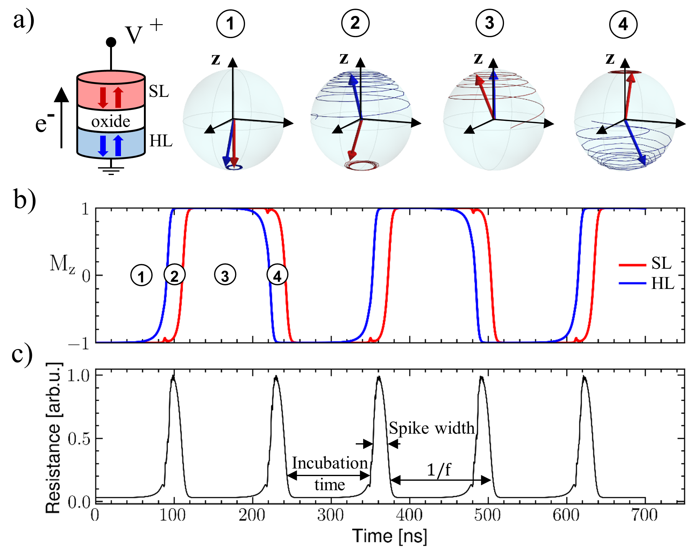
The structure of the spiking magnetic tunnel junction consists of two thin ferromagnetic layers with switchable magnetization oriented Out-Of-Plane (OOP) due to the perpendicular anisotropy induced at the interface with the Mg oxide spacer layer separating them 14, 15, 16 (see Fig. 1.a). Depending on the relative orientation of the magnetization of the two ferromagnetic layers, the junction resistance changes due to different tunneling probabilities of spin up and spin down electrons across the barrier, also called Tunnel Magneto Resistance effect 17. Here the two ferromagnetic layers have different anisotropy, leading to different stability. They are therefore called hard layer (HL) and soft layer (SL). Under sufficient applied voltage bias, dynamical states are created in which both hard layer (HL) and soft layer (SL) can switch by Spin-Transfer Torque (STT) 18, 19.
To illustrate this dynamics, two coupled macrospins (SL and HL) have been simulated with the effective anisotropy of SL lower than the one of HL (see supplementary material 1). The switching sequence of Fig. 1.b can be explained as follows: from the parallel (P) alignment of SL and HL pointing down , the reflected electrons (minority spin-up) at the interface between HL and the barrier forces the reversal of the HL from to , step . Subsequently, the SL reverses thanks to the spin-torque coming from the majority spin-up electrons of the HL passing through the barrier. Since the effective anisotropy of SL is smaller than the HL one, the reversal of the SL is faster. The two magnetizations retrieve a parallel alignment in the opposite up-direction with respect to the starting point . Without applying any external magnetic field, the reversal process is identical to . These magnetization switching sequences lead to a spiking behaviour of the electrical resistance. The characteristic lifetimes of the high and low resistance states are associated to the spike width and to the incubation time before spiking as illustrated in Fig. 1.c. In the following, the dynamics under a perpendicular applied field will be discussed and four characteristic times will be introduced that arise due to symmetry breaking of the magnetic orientations with respect to the applied external field.
In order to experimentally observe the spiking dynamics, p-MTJs with the composition shown in Fig. 2.a. are patterned into nanopillars of diameters ranging between 70 and 150 nm. The stack is deposited on thermally-oxidized single crystal Si(100) by DC magnetron sputtering with a base pressure of 10-8 mbar. On a 100mm wafer, the top (tSL) and bottom (tHL) FeCoB layers are deposited in the form of two orthogonal wedges, with thicknesses varying from 1.1 to 1.6 nm and from 0.6 to 1.0 nm, respectively. The thickness wedges allow the fabrication of devices with varying combinations of SL and HL thicknesses. Devices were patterned using Reactive Ion Etching (RIE) to create a Ta hardmask followed by an Ion Beam Etching (IBE) step to define the magnetic tunnel junction pillar. The resistance-area (RA) product is around 9 m² and TMR is 33% at low bias voltage. The device used in this demonstration has an electrical diameter of 90 nm and a parallel resistance of =1480 . The thinner FeCoB layer of the HL (tHL = 0.81nm) compared to the SL (tSL = 1.36nm) provides the desired asymmetry in effective anisotropy between the two layers.
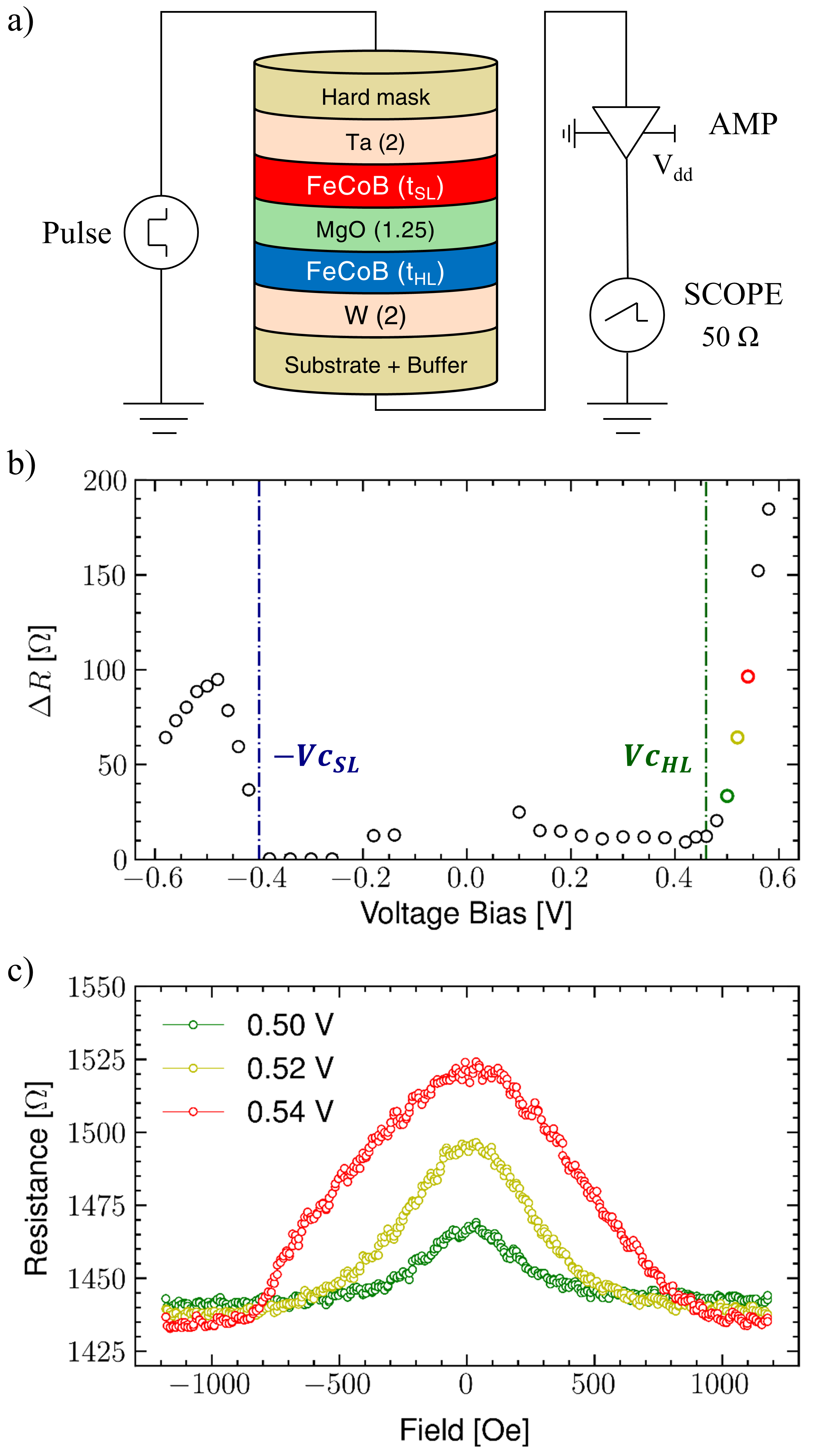
Before we discuss the time resolved measurements, we present quasi-static measurements of the magneto-resistance sweeping the applied magnetic field at different voltage biases. The resistance of the MTJ is measured in real time by sensing the current through the device with an oscilloscope using the voltage drop created on its internal 50 resistance after a 5 gain amplification (Fig. 2.a). The corresponding time-averaged resistance versus field curves are shown in Fig. 2.c and TMR versus voltage curve in Fig. 2.b. At low bias voltage, only the parallel state (P) is stabilized due to the dipolar coupling between the two layers. When increasing the positive bias voltage above a certain threshold (), the spin-polarized current provides enough torque to overcome the perpendicular anisotropy of both layers and their dipolar interaction, resulting in the dynamics described in Fig. 1. In this dynamical regime, the presence of high resistance spikes increases the average resistance of the device. As shown in Fig. 2.b, the device does not experience exactly the same response depending on the bias voltage polarity. In the negative polarity, the electrons flow from the soft layer (SL) to the hard layer (HL). Since for the device presented here, the critical voltage is slightly lower, with the spin current first flips the SL which results in the anti-parallel (AP) configuration. The windmill motion is then generated and stabilized when the applied voltage is larger than the critical voltage of the hard layer . It is noticed that, when the device has a small asymmetry between the effective anisotropy of the two layers, the two critical voltages are very close. Upon increasing the asymmetry between the two effective anisotropies, the junctions show distinct critical voltages and (see supplementary material 2). By applying an out-of-plane magnetic field, the windmill motion progressively turns into the saturation of the P state. The symmetry observed between positive and negative values of the applied magnetic field supports the claim that both layers are switching in the dynamical region. In fact, if one assumes that the dynamics comes from one layer only, an external magnetic field applied along the z-axis would result in a preferential P or AP state of the MTJ, which is not the case in our device. Additionally, we observe that the dynamics is more robust as the voltage bias increases, which is consistent with a spin-transfer torque driven reversal mechanism.
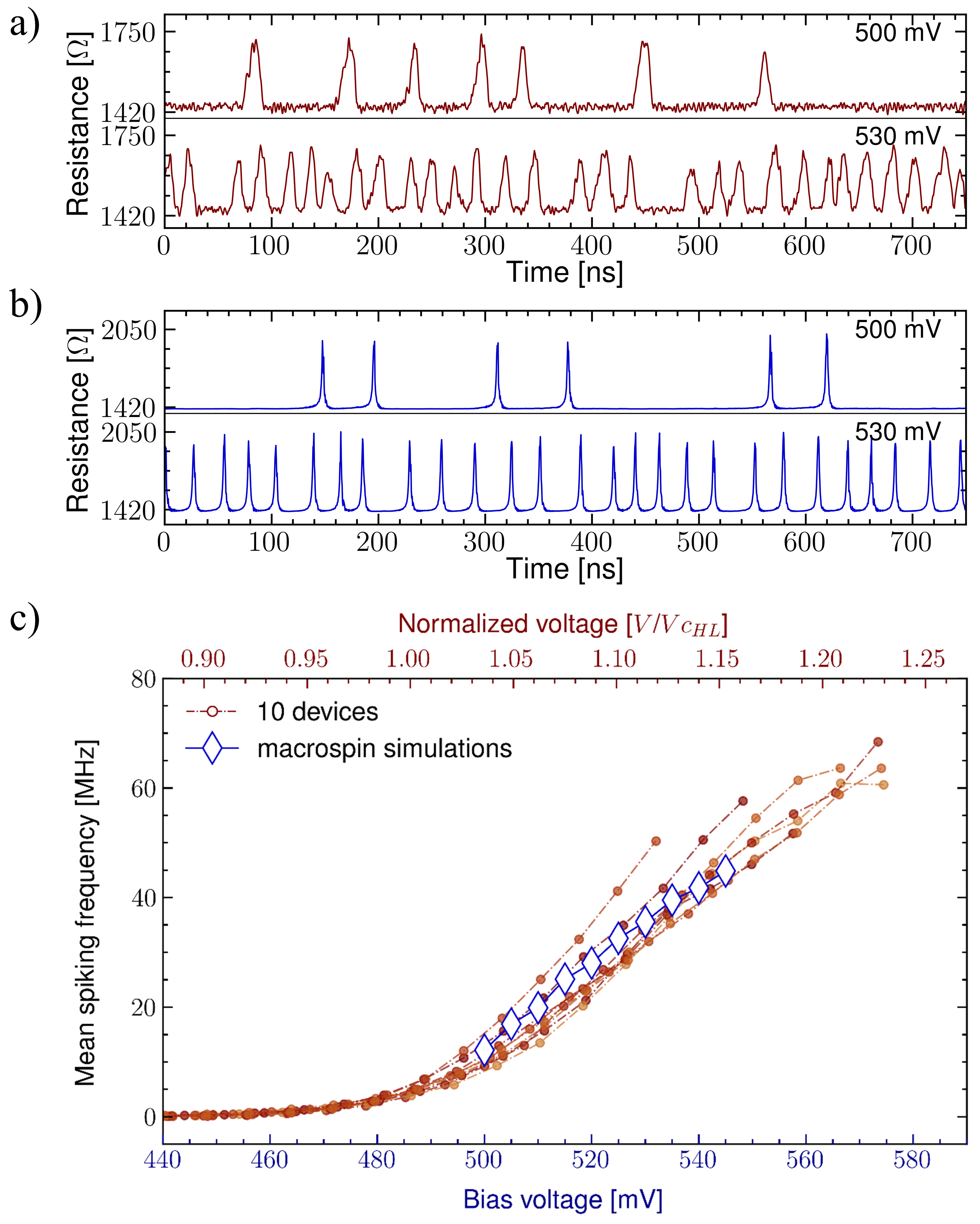
Time-resolved measurements were performed to address the dynamic features which confirm the origin of the resistance increase related to the continual switching between P and AP states. Typical time traces of a p-MTJ are shown in Fig. 3.a under a bias voltage of 500 and 530 mV. Measurements were performed on the same device as in Fig. 2. As expected, we retrieve short AP-state lifetimes and long P-state lifetimes, characteristic of a spiking response as the one shown in Fig. 1.c. To retrieve the mean spiking rate of our MTJ-neuron, we binarize the signal acquired into AP (), P () states and transitions between those states (). The spiking rate is then calculated as . Due to the predominant value of , the mean spiking rate behaves similarly to the inverse of the incubation time () and evolves non-linearly with the voltage bias (Fig. 3.c). This particular feature of the neuron activation function is a key ingredient needed in neural network application. The time-resolved measurements show very similar behaviour for 10 devices with diameter ranging from 70 to 150 nm. Macrospin simulations shown in Fig. 3.b (parameters given in supplementary material 1) and previous study 11 also demonstrate this behaviour with applied voltage and rule out the hypothesis of a purely super-paramagnetic stochastic switching response 20, 21, 22, 23 to explain our device behaviour.
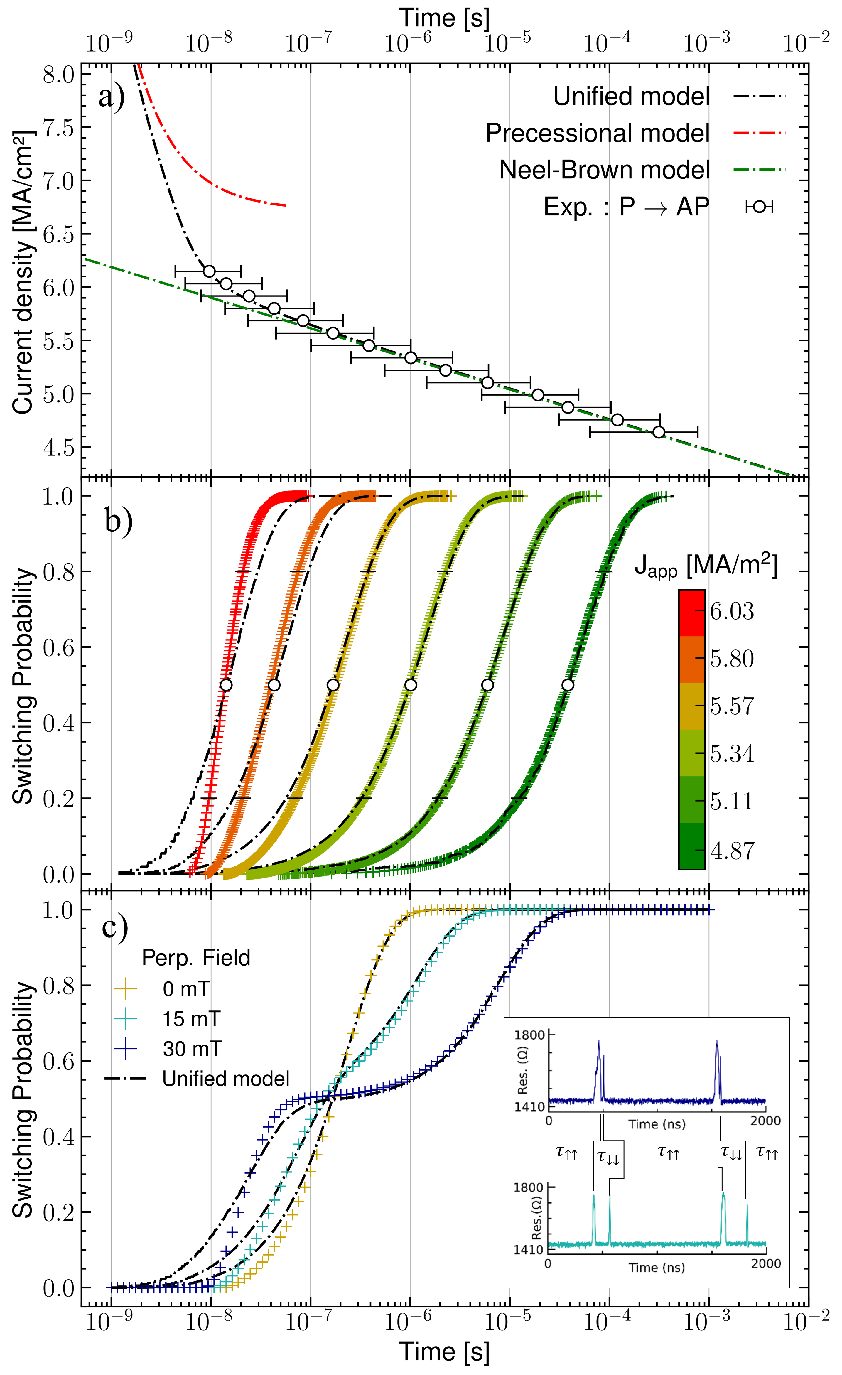
In order to assess the capabilities of large-scale neural networks and to design appropriate hardware circuits, it is essential to have adequate compact models. For this purpose, we have developed a compact model that depends on the critical parameters of our MTJ device. As the output mean frequency depends mainly on the incubation time, the model specifically focuses on how the incubation time changes with voltage bias and perpendicular external magnetic field. The incubation time between spikes varies significantly in the low current regime due to the stochastic nature of the STT switching in that regime. Below the critical bias voltage (), the dependence of this parameter with the applied current density is exponential 24. Above , the incubation time falls into a precessional regime 25, 26, 27 with a 1/V dependency. To combine the two regimes, we extended the model proposed by Yang et al. 28 by adding the term in the equation of the switching time to consider also the impact of an external magnetic field, as it has been proposed previously 29. The incubation time , related to the switching of the hard layer (HL), is expressed as function of the current density and of the perpendicularly applied field for a given switching probability :
| (1) |
where : , , and .
The term describes the switching time in the low current density regime (Neel-Brown model). The second term is representative of the precessional mode achieved in the higher current range. The spin-torque intensity , proposed by Yang et.al28, is used to merge the two models in a single expression and varies linearly from 0.25 to 0.15 in the range of the current density applied. The energy barrier (46 ), the characteristic times, (100 ns) and (270 ns), and the critical current density (6.71 ) are extracted from the fit of the cumulative distribution function (CDF) with the unified model Eq. (1) for current densities between 4.8 and 6.2 MA/cm². Fig. 4.a shows the median of the switching time from P state to AP state and the error bars correspond to the 20-80% range of the switching probability of the CDFs in Fig. 4.b. In the thermally assisted reversal case with long incubation times, the model accurately describes the experimental data. On the contrary, for very short lifetimes (), the fitting of the full CDF starts to deviate from device data. This can be explained to some extent by the 350 MHz bandwidth limitation of the amplifier used to provide signal gain, limiting the accuracy of measurements closer to the precessional regime.
As mentioned above, our dual structure is subject to the dipolar coupling. To evaluate its role, we performed systematic experiments under an external magnetic field to extract the dipolar field (12.2 mT) and the anisotropy field of the hard layer (147 mT). The external field affects the shape of the CDF since it brakes the symmetry between the two P states (, ) and the two AP states (, ), leading to four different characteristic times : . At a given current density and for a positive applied magnetic field (+z), and times decrease because the field polarity helps magnetization reversals from to configuration due to the Zeeman energy. Whereas the and times increase because the positive applied field hinders the magnetization to switch from to orientation. The consequences of the external applied field on the signal acquired are shown in the inset of Fig. 4.c where a long P state () is followed by a shorter P state (). The asymmetries between the two P states and the two AP states increase with the field amplitude. The plateau at 50% of probability in Fig. 4.c confirms that there is the same number of short and long P states when the applied field significantly changes the associated characteristic times . This is an additional proof that the windmill dynamics drives the spiking response of the device.
The robustness of the windmill dynamics with respect to the external magnetic field is an important requirement for device integration as both their number and density increase. Indeed, neuromorphic computing generally requires millions of neurons and synapses in a limited area for embedded applications which may create stray field interactions between devices. Even if the shape of the CDF is modified with external applied magnetic field, the spiking feature remains, as confirmed by the time traces in the inset of Fig. 4.c. From another viewpoint, one may see the external field as an additional degree of freedom to tune the probability distribution of the spiking signal. To conserve the high energy efficiency 30 of analog neuromorphic circuits with respect to other computing schemes, the energy consumption at the device level must be evaluated. The energy needed to produce one single spike in our device, was calculated as , showing values of 4 to 16 pJ in a frequency range from 10 to 50 MHz. State-of-art STT-RAM achieves nowadays switching reversal below 100 fJ 31, 32 with high stability (). This energy per operation could further decrease by reducing the effective magnetic anisotropy of the layers as our proposed device does not require any high stability layer. Furthermore, several issues arising from the SAF element in conventional STT-RAM are avoided, such as the use of critical materials 33, the additional complexity to combine different crystal orientations 34 and the limited thermal budget due to atom migration 35. A CMOS-compatible two-terminal device with a simple material stack, not requiring a SAF reference, and operating without set/reset or compensation applied magnetic fields are strong benefits of our solution. These demonstration of the spiking functionality with device diameters down to 70 nm opens a concrete path to design dense arrays for in-memory computing.
In summary, we demonstrated the use of a dual free layer MTJ to generate electrical spiking signals under an applied bias voltage. The output spiking frequency is a non-linear activation function with respect to the external excitation as required in NN algorithms. Simulations and multiple experimental data sets converge to explain the origin of the spikes as the generation of a windmill-like magnetization reversal sequence. Towards hardware circuit design, we develop a compact model that describe our experimental data combining both thermally activated and precessional switching regimes. The possible impact of stray fields in dense arrays was shown to be negligible, as demonstrated by the resilience of the windmill dynamic under applied magnetic field up to 30 mT. The low power consumption (4-16 pJ/spike) and high scalability of this MTJ-based spiking neuron ( 80 nm) presents a concrete solution for the implementation of SNN in hardware at the nanoscale.
This work was supported by ANR via grant SpinSpike Projet-ANR-20-CE24-0002.
The data that support the findings of this study are available from the corresponding author upon reasonable request.
References
- Marković et al. 2020 Marković, D.; Mizrahi, A.; Querlioz, D.; Grollier, J. Physics for neuromorphic computing. Nature Reviews Physics 2020, 2, 499–510, Number: 9 Publisher: Nature Publishing Group
- Tavanaei et al. 2019 Tavanaei, A.; Ghodrati, M.; Kheradpisheh, S. R.; Masquelier, T.; Maida, A. Deep learning in spiking neural networks. Neural Networks 2019, 111, 47–63
- Serrano-Gotarredona et al. 2013 Serrano-Gotarredona, T.; Masquelier, T.; Prodromakis, T.; Indiveri, G.; Linares-Barranco, B. STDP and STDP variations with memristors for spiking neuromorphic learning systems. Frontiers in Neuroscience 2013, 7
- Martin et al. 2021 Martin, E.; Ernoult, M.; Laydevant, J.; Li, S.; Querlioz, D.; Petrisor, T.; Grollier, J. EqSpike: Spike-driven equilibrium propagation for neuromorphic implementations. iScience 2021, 24, 102222
- Davies et al. 2018 Davies, M. et al. Loihi: A Neuromorphic Manycore Processor with On-Chip Learning. IEEE Micro 2018, 38, 82–99
- Furber et al. 2014 Furber, S. B.; Galluppi, F.; Temple, S.; Plana, L. A. The SpiNNaker Project. Proceedings of the IEEE 2014, 102, 652–665
- Benjamin et al. 2014 Benjamin, B. V.; Gao, P.; McQuinn, E.; Choudhary, S.; Chandrasekaran, A. R.; Bussat, J.-M.; Alvarez-Icaza, R.; Arthur, J. V.; Merolla, P. A.; Boahen, K. Neurogrid: A Mixed-Analog-Digital Multichip System for Large-Scale Neural Simulations. Proceedings of the IEEE 2014, 102, 699–716
- De Marinis et al. 2019 De Marinis, L.; Cococcioni, M.; Castoldi, P.; Andriolli, N. Photonic Neural Networks: A Survey. IEEE Access 2019, 7, 175827–175841, Conference Name: IEEE Access
- Nandakumar et al. 2020 Nandakumar, S. R.; Boybat, I.; Le Gallo, M.; Eleftheriou, E.; Sebastian, A.; Rajendran, B. Experimental Demonstration of Supervised Learning in Spiking Neural Networks with Phase-Change Memory Synapses. Scientific Reports 2020, 10, 8080, Number: 1 Publisher: Nature Publishing Group
- Mizrahi et al. 2018 Mizrahi, A.; Hirtzlin, T.; Fukushima, A.; Kubota, H.; Yuasa, S.; Grollier, J.; Querlioz, D. Neural-like computing with populations of superparamagnetic basis functions. Nature Communications 2018, 9, 1533, Number: 1 Publisher: Nature Publishing Group
- Matsumoto et al. 2019 Matsumoto, R.; Lequeux, S.; Imamura, H.; Grollier, J. Chaos and Relaxation Oscillations in Spin-Torque Windmill Spiking Oscillators. Physical Review Applied 2019, 11, 044093
- Choi et al. 2016 Choi, R.; Katine, J. A.; Mangin, S.; Fullerton, E. E. Current-Induced Pinwheel Oscillations in Perpendicular Magnetic Anisotropy Spin Valve Nanopillars. IEEE Transactions on Magnetics 2016, 52, 1–5
- Thomas et al. 2017 Thomas, L. et al. Spin Transfer Torque driven dynamics of the synthetic antiferromagnetic reference layer of perpendicular MRAM devices. 2017 IEEE International Magnetics Conference (INTERMAG). Dublin, Ireland, 2017; pp 1–1
- Dieny and Chshiev 2017 Dieny, B.; Chshiev, M. Perpendicular magnetic anisotropy at transition metal/oxide interfaces and applications. Reviews of Modern Physics 2017, 89, 025008, Publisher: American Physical Society
- Kishi et al. 2008 Kishi, T. et al. Lower-current and fast switching of a perpendicular TMR for high speed and high density spin-transfer-torque MRAM. 2008 IEEE International Electron Devices Meeting. 2008; pp 1–4, ISSN: 2156-017X
- Ikeda et al. 2010 Ikeda, S.; Miura, K.; Yamamoto, H.; Mizunuma, K.; Gan, H. D.; Endo, M.; Kanai, S.; Hayakawa, J.; Matsukura, F.; Ohno, H. A perpendicular-anisotropy CoFeB–MgO magnetic tunnel junction. Nature Materials 2010, 9, 721–724, Number: 9 Publisher: Nature Publishing Group
- Julliere 1975 Julliere, M. Tunneling between ferromagnetic films. Physics Letters A 1975, 54, 225–226
- Slonczewski 1996 Slonczewski, J. Current-driven excitation of magnetic multilayers. Journal of Magnetism and Magnetic Materials 1996, 159, L1–L7
- Berger 1996 Berger, L. Emission of spin waves by a magnetic multilayer traversed by a current. Physical Review B 1996, 54, 9353–9358
- Sengupta et al. 2016 Sengupta, A.; Panda, P.; Wijesinghe, P.; Kim, Y.; Roy, K. Magnetic Tunnel Junction Mimics Stochastic Cortical Spiking Neurons. Scientific Reports 2016, 6, 30039, Number: 1 Publisher: Nature Publishing Group
- Bapna and Majetich 2017 Bapna, M.; Majetich, S. A. Current control of time-averaged magnetization in superparamagnetic tunnel junctions. Applied Physics Letters 2017, 111, 243107
- Parks et al. 2018 Parks, B.; Bapna, M.; Igbokwe, J.; Almasi, H.; Wang, W.; Majetich, S. A. Superparamagnetic perpendicular magnetic tunnel junctions for true random number generators. AIP Advances 2018, 8, 055903
- Camsari et al. 2017 Camsari, K. Y.; Faria, R.; Sutton, B. M.; Datta, S. Stochastic $p$-Bits for Invertible Logic. Physical Review X 2017, 7, 031014, Publisher: American Physical Society
- Brown 1963 Brown, W. F. Thermal Fluctuations of a Single-Domain Particle. Physical Review 1963, 130, 1677–1686
- Sun 2000 Sun, J. Z. Spin-current interaction with a monodomain magnetic body: A model study. Physical Review B 2000, 62, 570–578
- Koch et al. 2004 Koch, R. H.; Katine, J. A.; Sun, J. Z. Time-Resolved Reversal of Spin-Transfer Switching in a Nanomagnet. Physical Review Letters 2004, 92, 088302
- He et al. 2007 He, J.; Sun, J. Z.; Zhang, S. Switching speed distribution of spin-torque-induced magnetic reversal. Journal of Applied Physics 2007, 101, 09A501
- Yang et al. 2022 Yang, X.; Zhang, Y.; Zhang, Y.; Wang, P. A Universal Compact Model for Spin-Transfer Torque-Driven Magnetization Switching in Magnetic Tunnel Junction. IEEE Transactions on Electron Devices 2022, 69, 6453–6458
- Tomita et al. 2013 Tomita, H.; Miwa, S.; Nozaki, T.; Yamashita, S.; Nagase, T.; Nishiyama, K.; Kitagawa, E.; Yoshikawa, M.; Daibou, T.; Nagamine, M.; Kishi, T.; Ikegawa, S.; Shimomura, N.; Yoda, H.; Suzuki, Y. Unified understanding of both thermally assisted and precessional spin-transfer switching in perpendicularly magnetized giant magnetoresistive nanopillars. Applied Physics Letters 2013, 102, 042409
- Grollier et al. 2020 Grollier, J.; Querlioz, D.; Camsari, K. Y.; Everschor-Sitte, K.; Fukami, S.; Stiles, M. D. Neuromorphic spintronics. Nature Electronics 2020, 3, 360–370
- Wang et al. 2013 Wang, K. L.; Alzate, J. G.; Amiri, P. K. Low-power non-volatile spintronic memory: STT-RAM and beyond. Journal of Physics D: Applied Physics 2013, 46, 074003, Publisher: IOP Publishing
- Zeng et al. 2011 Zeng, Z. M.; Khalili Amiri, P.; Rowlands, G.; Zhao, H.; Krivorotov, I. N.; Wang, J.-P.; Katine, J. A.; Langer, J.; Galatsis, K.; Wang, K. L.; Jiang, H. W. Effect of resistance-area product on spin-transfer switching in MgO-based magnetic tunnel junction memory cells. Applied Physics Letters 2011, 98, 072512
- Palomino et al. 2021 Palomino, A.; Marty, J.; Auffret, S.; Joumard, I.; Sousa, R. C.; Prejbeanu, I. L.; Ageron, B.; Dieny, B. Evaluating critical metals contained in spintronic memory with a particular focus on Pt substitution for improved sustainability. Sustainable Materials and Technologies 2021, 28, e00270
- Djayaprawira et al. 2005 Djayaprawira, D.; Tsunekawa, K.; Nagai, M.; Maehara, H.; Yamagata, S.; Watanabe, N.; Yuasa, S.; Suzuki, Y.; Ando, K. 230% room-temperature magnetoresistance in CoFeB/MgO/CoFeB magnetic tunnel junctions. Applied Physics Letters 2005, 86, 092502–092502
- Karthik et al. 2012 Karthik, S. V.; Takahashi, Y. K.; Ohkubo, T.; Hono, K.; Gan, H. D.; Ikeda, S.; Ohno, H. Transmission electron microscopy study on the effect of various capping layers on CoFeB/MgO/CoFeB pseudo spin valves annealed at different temperatures. Journal of Applied Physics 2012, 111, 083922, Publisher: American Institute of Physics