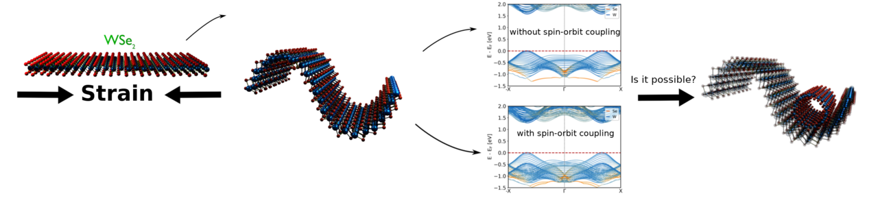
Funneling and spin-orbit coupling in transition-metal dichalcogenide nanotubes and wrinkles
Abstract
Strain engineering provides a powerful means to tune the properties of two-dimensional materials. Accordingly, numerous studies have investigated the effect of bi- and uniaxial strain. Yet, the strain fields in many systems such as nanotubes and nanoscale wrinkles are intrinsically inhomogeneous and the consequences of this symmetry breaking are much less studied. Understanding how this affects the electronic properties is crucial especially since wrinkling is a powerful method to apply strain to two-dimensional materials in a controlled manner. In this paper, we employ density functional theory to understand the correlation between the atomic and the electronic structure in nanoscale wrinkles and nanotubes of the prototypical transition metal dichalcogenide \ceWSe2. Our research shows that the symmetry breaking in these structures leads to strong Rashba-like splitting of the bands at the point and they thus may be utilized in future tunable spintronic devices. The inhomogeneous strain reduces the band gap and leads to a localization of the band edges in the highest-curvature region, thus funneling excitons there. Moreover, we show how wrinkles can be modeled as nanotubes with the same curvature and when this comparison breaks down and further inhomogenities have to be taken into account.
I Introduction
Two-dimensional (2D) materials have been the focus of a myriad of researches in the last decade due to their fascinating properties. After the successful synthesis of graphene [1] other materials such as hexagonal Boron nitride (h-BN) [2], transition metal dichalcogenides (TMDCs) [3, 4, 5, 6] and black phosphorous [7] joined the class of 2D materials quite quickly. Many researchers investigated the intriguing properties of this new class of materials such as their extraordinary strength and high deformation before rupture, high mobility, and ease of property alteration [8, 9, 10, 11, 12, 13, 14]. 2D materials proved to be useful for many applications such as nanoelectronics, spintronics, and catalysis [15, 16, 17, 18].
Still, researchers are trying to expand the applicability of these materials by methods such as alloying [19], introduction of defects [20], creation of van der Waals heterostructures or by applying external pressure and fields [21, 22]. Another method offering a reversible and non-destructive route to modulate the properties of 2D materials is strain engineering.[23, 24, 25, 26, 27, 28, 29, 30] Uniaxial and biaxial strains have been studied extensively [31, 32] and there are standard techniques which can be used already during the synthetization of 2D materials [12]. Often the application of in-plane stress will lead to the formation of wrinkles and there are established methods to produce these wrinkles [33] which can even be used to determine the mechanical properties of the layered material [34, 35, 36]. Furthermore, the changes of the electronic structure in these wrinkles leads to funneling, i.e., a preferential emission of light from certain spatial position along the wrinkle.[28, 37, 38, 39, 40, 30] However, the local strain in such samples is far from being homogeneous and the comparison with calculations of homogeneously strained systems might be misleading. Understanding this (local) inhomogeneous strain in 2D materials requires further research due to the vast opportunities for future applications such as polarized single photon emitters [41, 42] and flexible optoelectronics [23].
In order to understand the influence of the inhomogeneous strain in 2D systems one can study idealized model systems which have a similar strain state but are easier to control from an experimental point of view or need less approximations in the respective theoretical description. Nanotubes (NTs) are structures where strain fields can play an important role [43, 44] and even though those are not strictly inhomogeneous, since the strain can be defined by a constant curvature, they represent such a simple model system which is different from the uni- or biaxially strained 2D layers and closer to the wrinkled systems in experiments.
The investigation of the electronic properties of inhomogeneously strained materials requires methods such as density functional theory (DFT) or density functional based tight binding (DFTB) which can be computationally demanding for large systems. Fortunately, for NTs, researchers have developed a method to reduce the size of the curved systems – cyclic DFT [45, 46, 47] employs the helical boundary condition in nanotubes in order to reduce the cost of the calculation and the method was successfully used to determine the bending modulus of various 2D systems. Yet, to the best of our knowledge, no one investigated the similarities and differences of NTs and wrinkles even if this understanding is crucial as in larger wrinkles (or other system where the variation of strain is due to a variation of the local curvature) it is computationally impossible to model the system entirely. NTs could then be used to further simplify the calculation by the use of cyclic DFT.
The sheer size of inhomogeneously strained structures causes many theoretical investigations to neglect relativistic effects beyond scalar-relativistic limits in order to enhance computational speed. Including spin-orbit coupling (SOC) in systems with heavy elements (like TMDCs) is however very important to understand many fascinating physical effects occurring in 2D materials such as the Hall effect at room temperature [48], the Rashba effect [49, 50] and spin-valley coupling [51].
The Rashba effect, i.e., the emergence of spin splitting in momentum direction, [49, 52] occurs due to inversion symmetry breaking in the presence of SOC. Such splitting was initially observed in zinc blends, wurtzite, and in systems under an external electric field. Another type of system in which this splitting is observed, is Janus-type 2D materials due to the resulting internal electric field perpendicular to the structure. Yet, the internal electric field and the subsequent splitting are quite small (). Cheng et al. [53] studied such polar TMDCs (\ceWSSe as an example) proving their stability and recommended them to be used for Datta-Das spin field effect transistors. This behavior can be even more interesting if the splitting manifests adjustability without the need of an external electric field. Yao et al. [54] utilized biaxial strain to manipulate the Rashba splitting in Janus heterostructures and concluded that the change of orbital overlaps increases the splitting. Since many symmetries including inversion symmetry are broken in curved systems such as NTs and wrinkles, one could also imagine the emergence of similar phenomena especially since such a curvature-induced SOC has already been shown for carbon NTs.[55, 56]
Having mentioned the importance of inhomogeneous strain in 2D structures, in this paper, we investigate \ceWSe2 in the form of NTs and wrinkles theoretically. We concentrate on these systems specifically since we also want to estimate if and when NTs can be used to model large scale wrinkles in order to ease the computational load using helical boundary conditions. The similarities between NTs and wrinkles are expounded and strain associated phenomena in the band structures are described. We explore NTs and wrinkles in ranges larger than any previous investigation to the best of our knowledge with an ab initio method including SOC effects which provides electronic insight about these materials for better future applications.
II Results and discussion
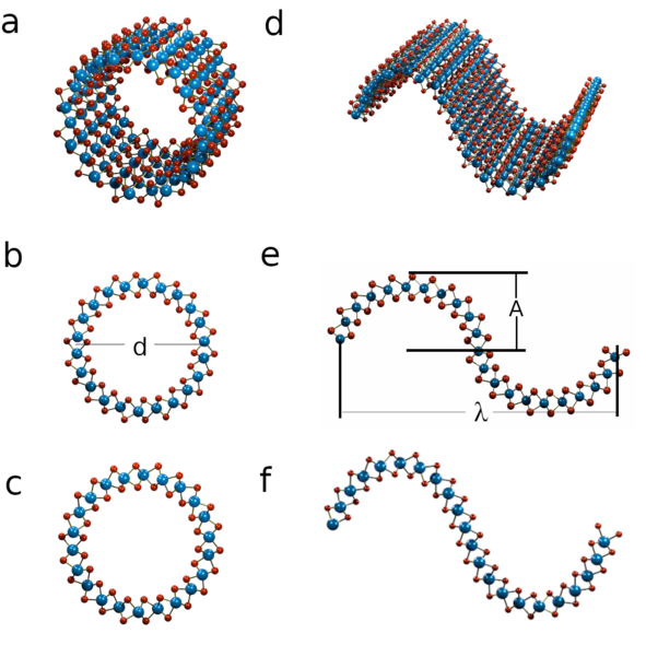
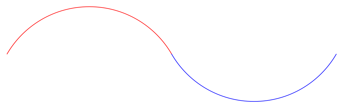
In the following, we will investigate how inhomogeneous strain affects wrinkles and NTs of monolayer \ceWSe2 – a prototypical example of the TMDCs. In order to compare wrinkles and NTs, the initial wrinkled structure was created with a circular profile as shown in Figure 1 with a wavelength to amplitude ratio of and using NTs as input. We will discuss the deformation energy and changes in the band dispersion and we will explain the origin of funneling in nanoscale wrinkles as well as a Rashba-like splitting that occurs in curved TMDC structures. We will further explain in detail the similarities of electronic structure of NTs and wrinkles.
II.1 Deformation energy/band gaps
The relaxation of the initial structure is very different for NTs and wrinkles. While the former only change the diameter (cf., Figures 1b and 1c), the latter relax into structures which do not resemble the initial nanotube-like profile anymore (Figures 1e and 1f), especially in the region close to the middle plane of the unit cell (inflection point). In this region, the wrinkled structure resembles a flat monolayer and is thus under less local strain in comparison to the corresponding nanotube. However, the peak of the wrinkles deforms stronger, leading to areas with higher curvature. The curvature in NTs on the other hand is constant since they always remain circular (Figure 1c).
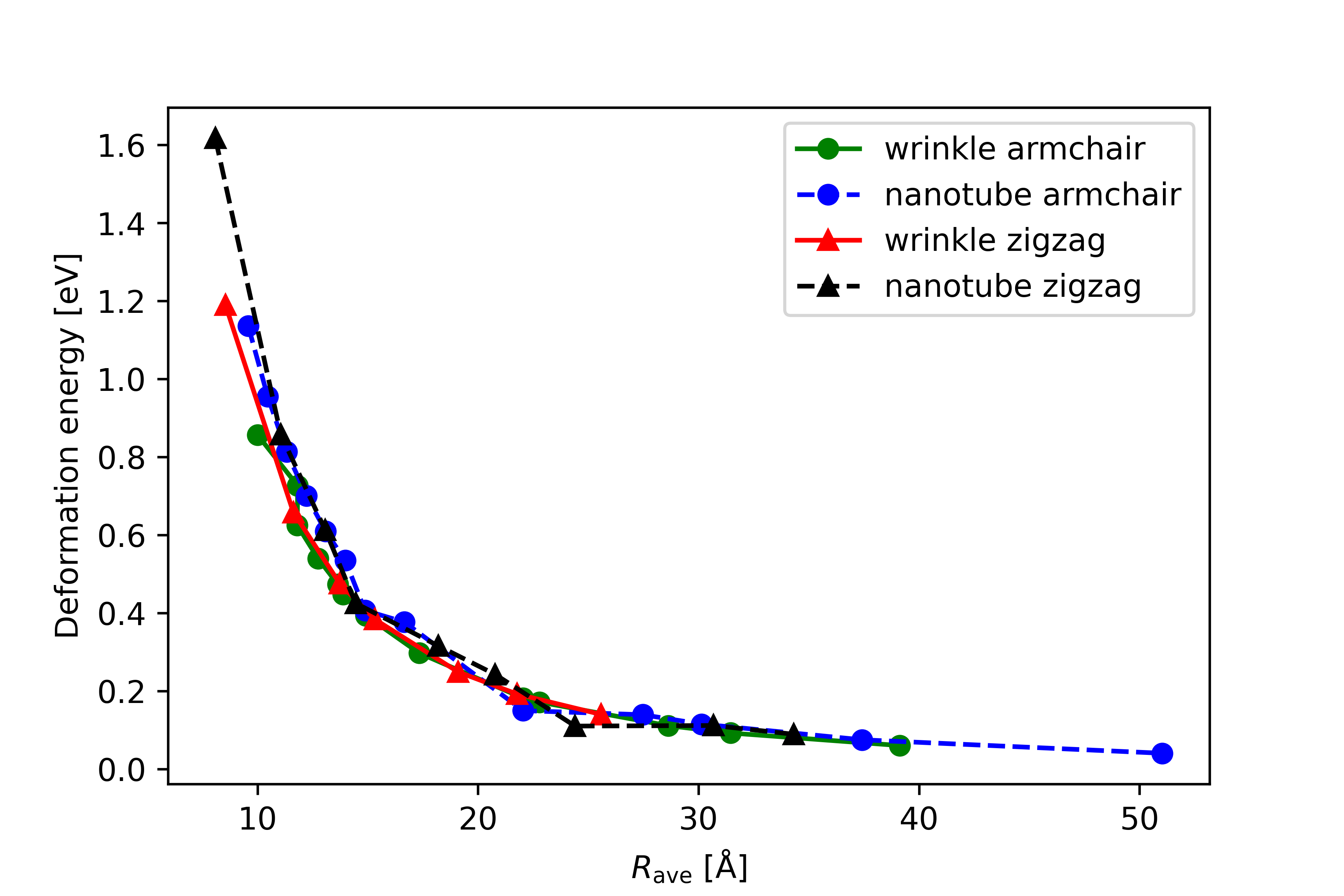
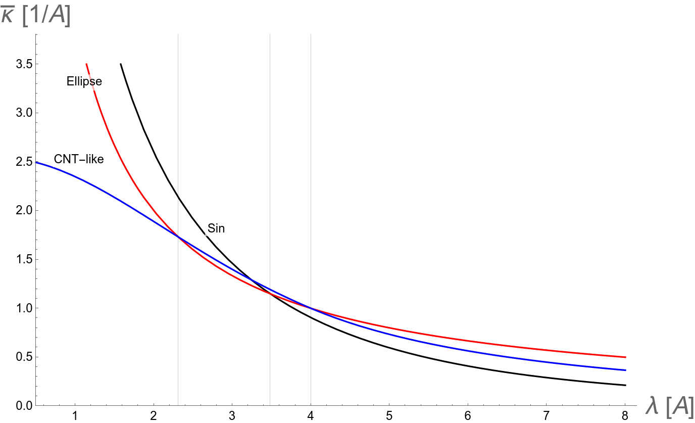
In order to allow for a better comparison between NTs and wrinkles, we will introduce two new measures – the average and the maximum radius of curvature, and – by fitting a spline to the positions of the tungsten atoms and calculating its curvature. The comparison of the deformation energies, , as function of the average radius of curvature in Figure 2 shows that there is a small difference between NTs and wrinkles for the smaller systems (i.e., with larger average curvature) while the difference between armchair and zigzag is negligible. The deformation energy, , has been calculated as follows:
| (1) |
where is the energy of the wrinkle/nanotube, is the number of formula units, and is the energy of the flat monolayer. This indicates that the local relaxation at the inflection point of the wrinkles and the corresponding increasing curvature at the maxima can be understood as a redistribution of the strain which leads to a total energy gain. Figure 2 furthermore shows that this energy gain (per formula unit) becomes very small for .
Interestingly, the profile of the relaxed wrinkles differs from the sinusoidal wave which is assumed in continuum mechanics and which follows from the harmonic approximation. The deviation from the sinusoidal shape is more prominent for shorter wavelengths and vanishes for wrinkles with larger wavelength which are more similar to monolayers. In fact, the long-range behavior is expected and can already be predicted by analyzing the average curvature of differently wrinkled curves (see section “Curvature analysis” in the supporting information (SI) for more details [57]). In brief, for the profile tends to be sinusoidal, while for smaller an elliptical or circular profile is preferred. This deviation from the harmonic solution is important for analyzing the strain fields using electron microscopy images for which one requires an assumption about the shape of the wrinkle (cf., Refs. 58, 59).
Our structures with after relaxation are in fact better fitted by two sine functions with one having an almost three times larger wavelength.
Such wrinkle profiles, having periodically wrinkled areas with peaks and valleys have already been observed in wrinkling experiments on polymeric substrate [22, 35]. Yet, in other wrinkling experiments [60], single wrinkles with only peaks connected with areas of lower strain have been found. In order to keep the discussions in this paper general, we focus on fully relaxed wrinkles which correspond to the expected relaxed freestanding wrinkle profile. The investigation of substrate-induced effects is an interesting topic which is however beyond the current investigation.
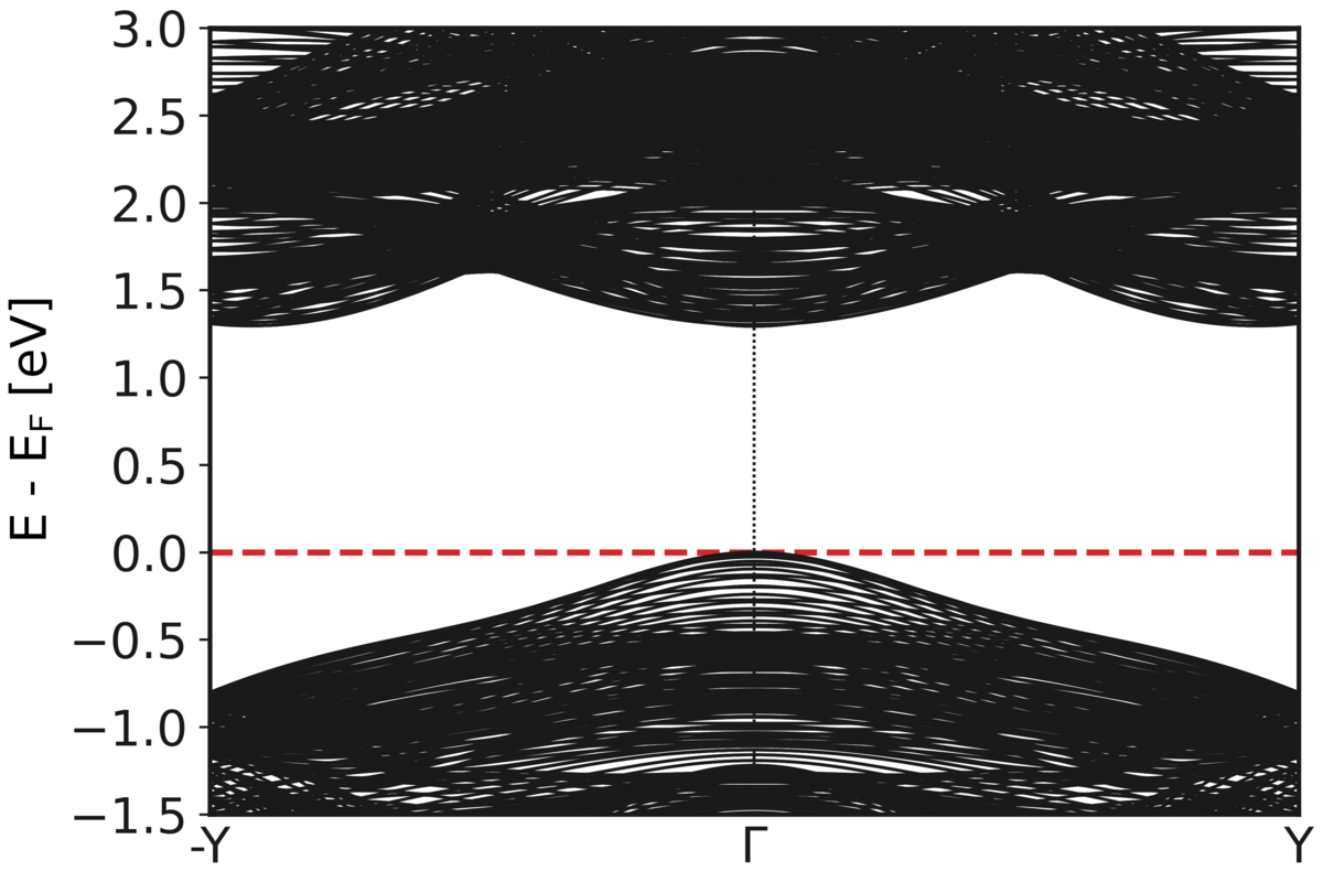
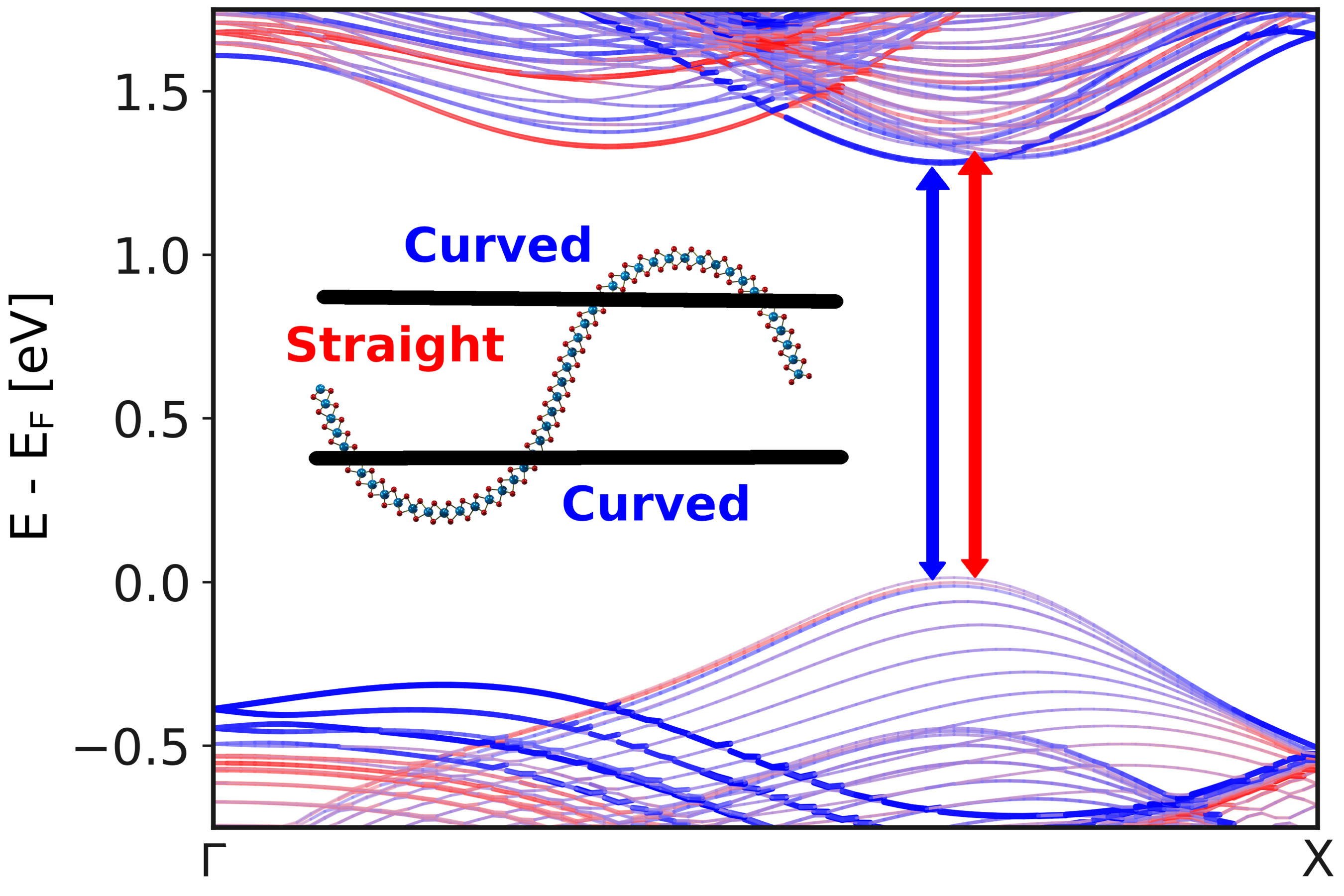
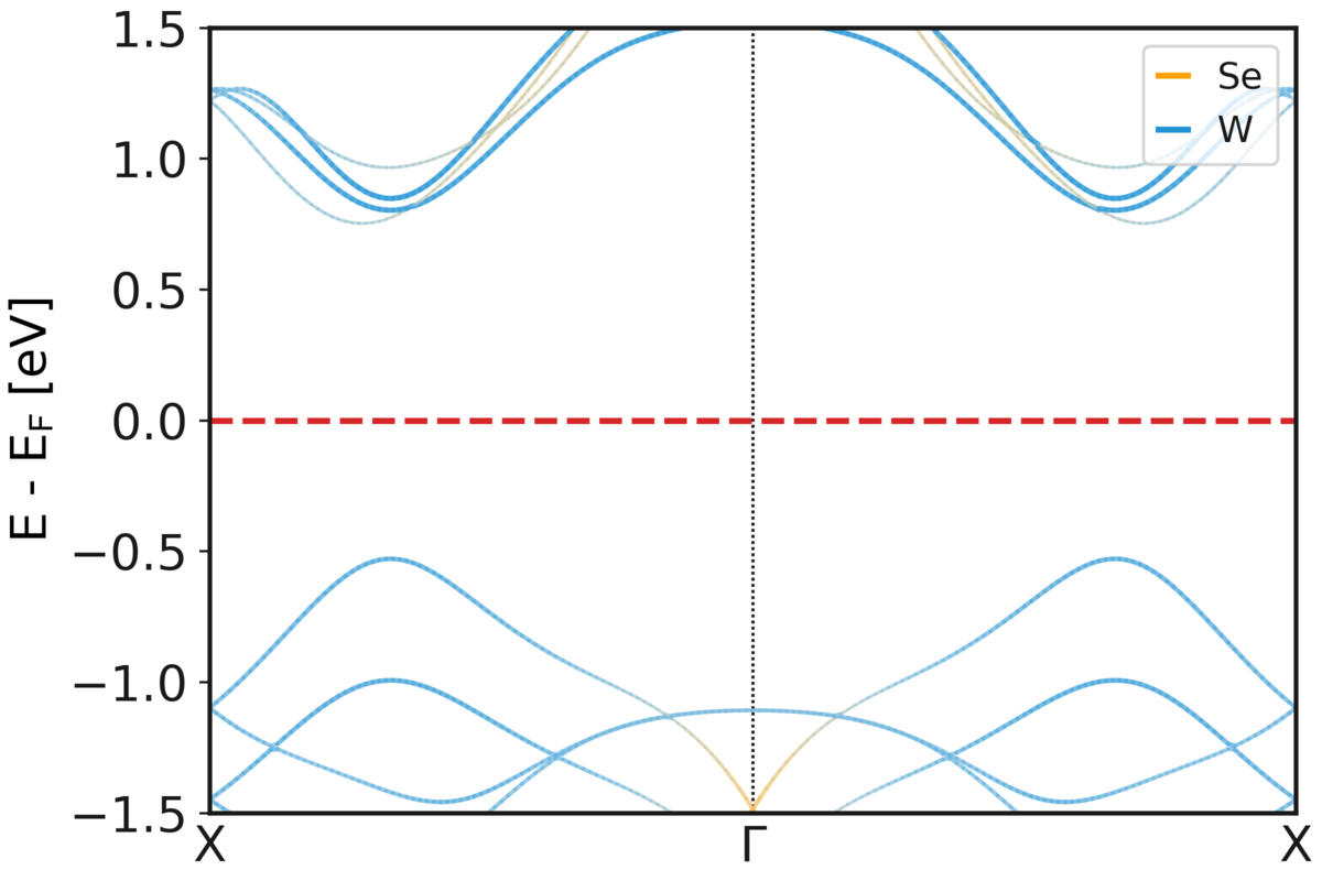
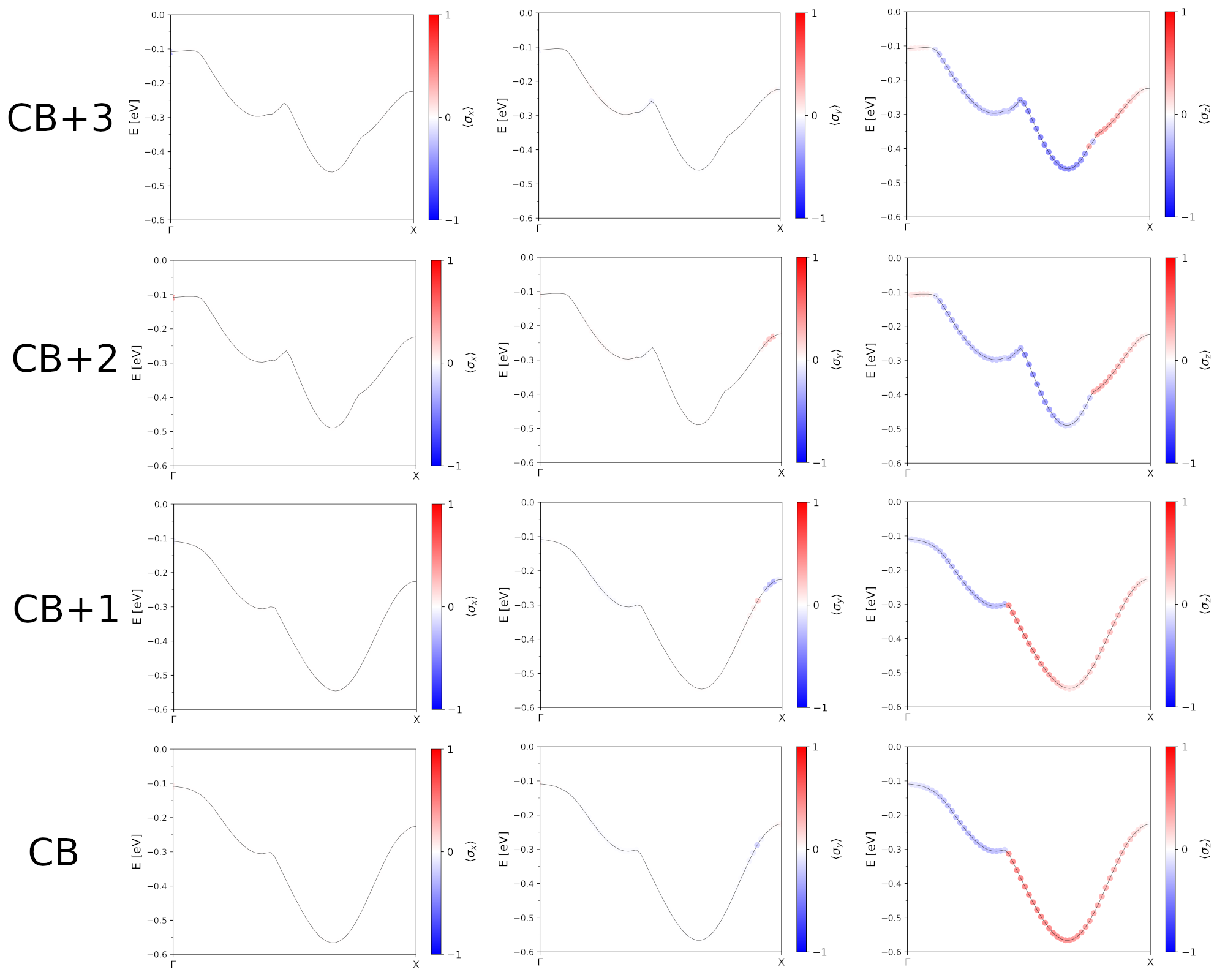
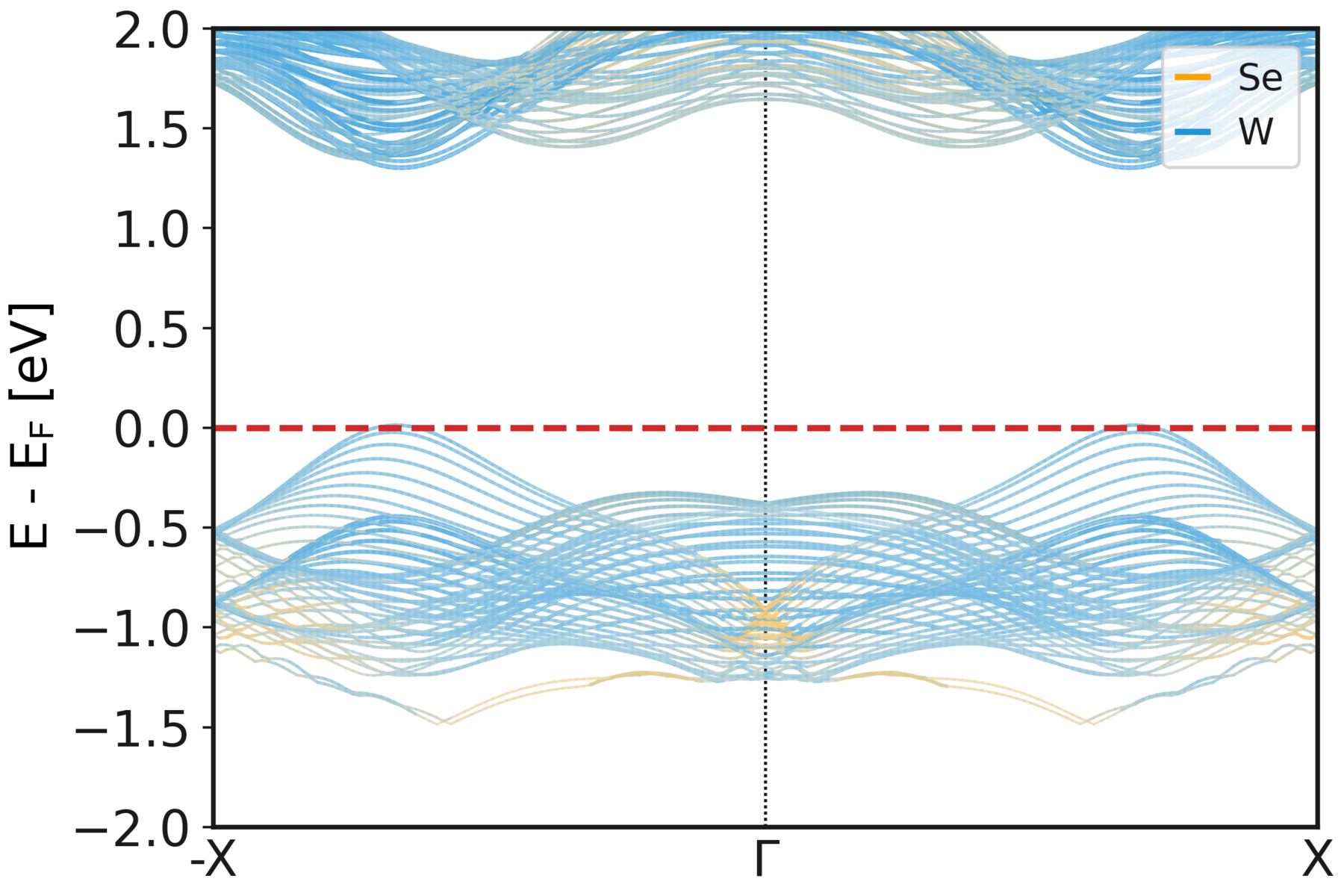
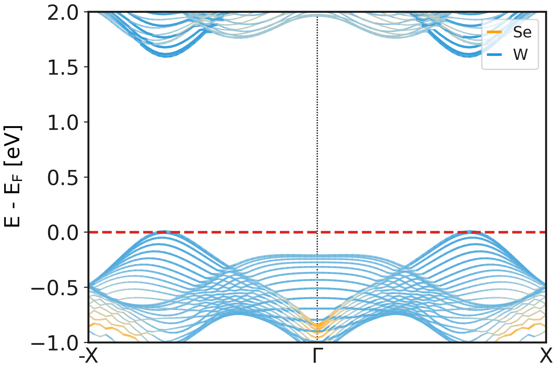
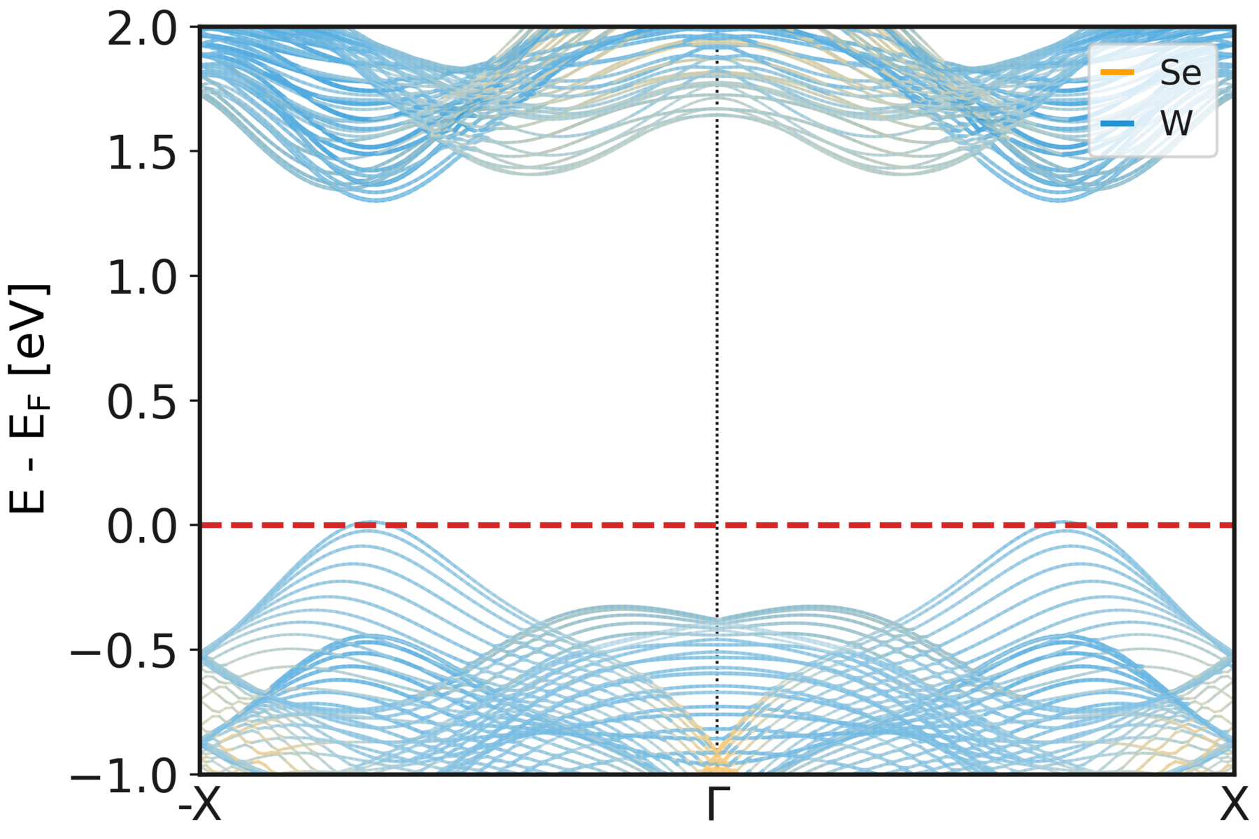
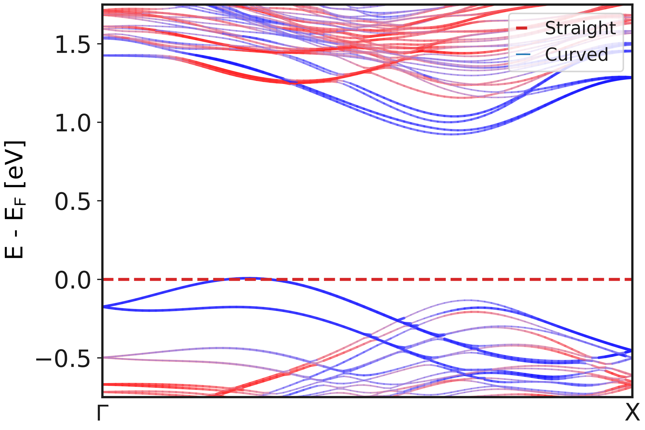
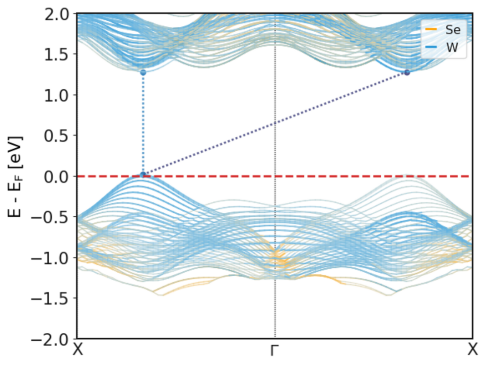
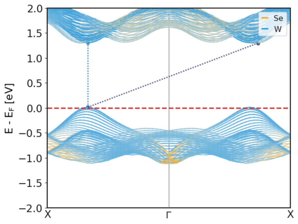
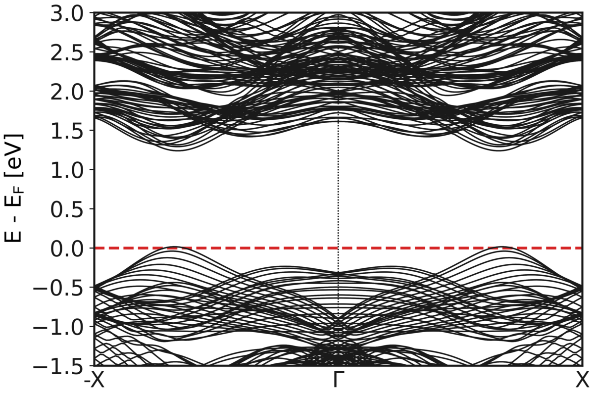
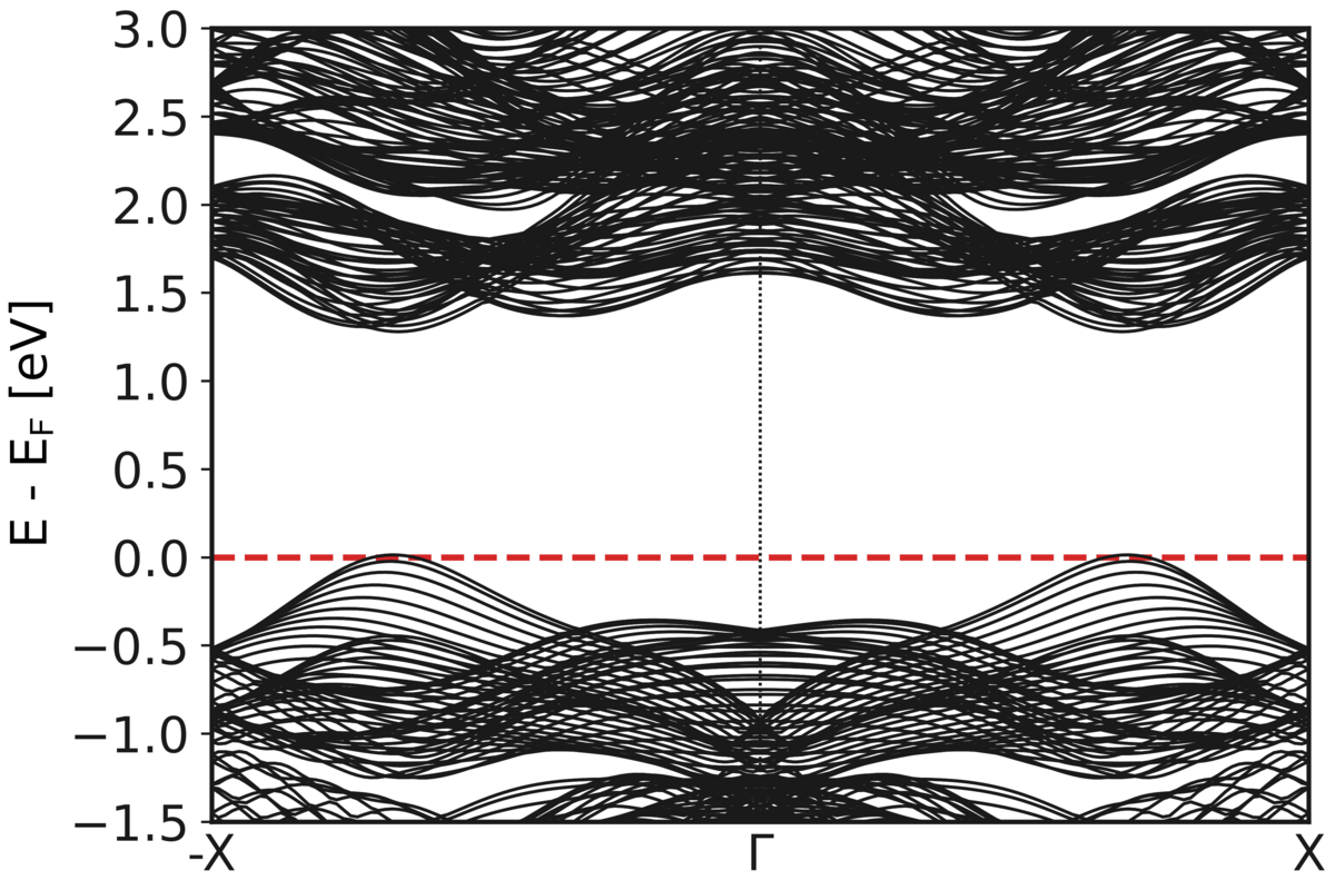
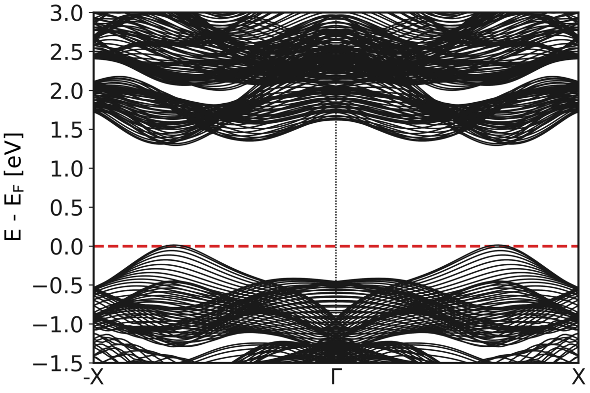
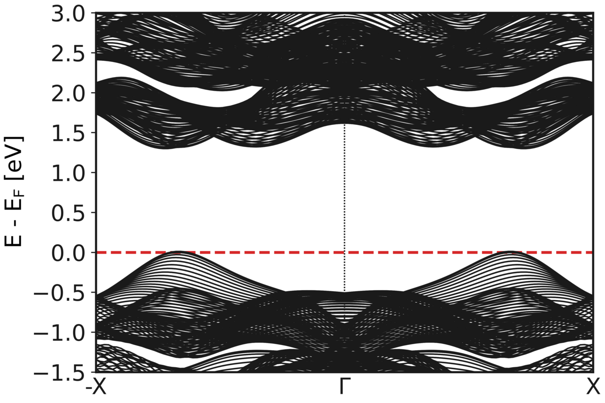
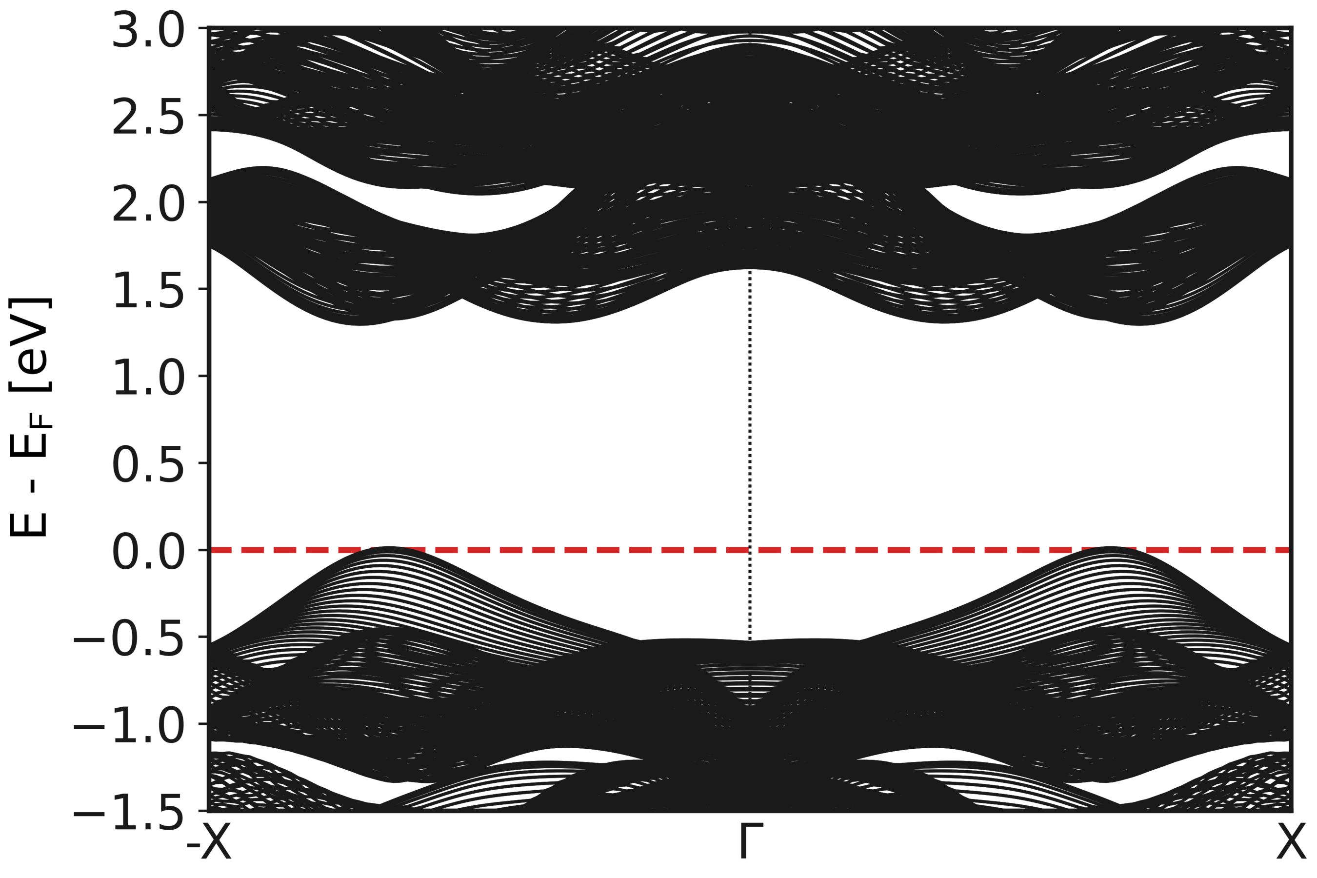
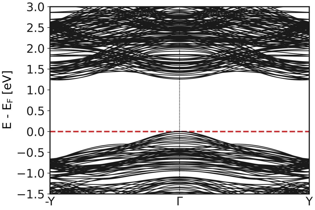
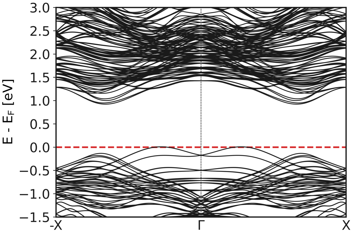
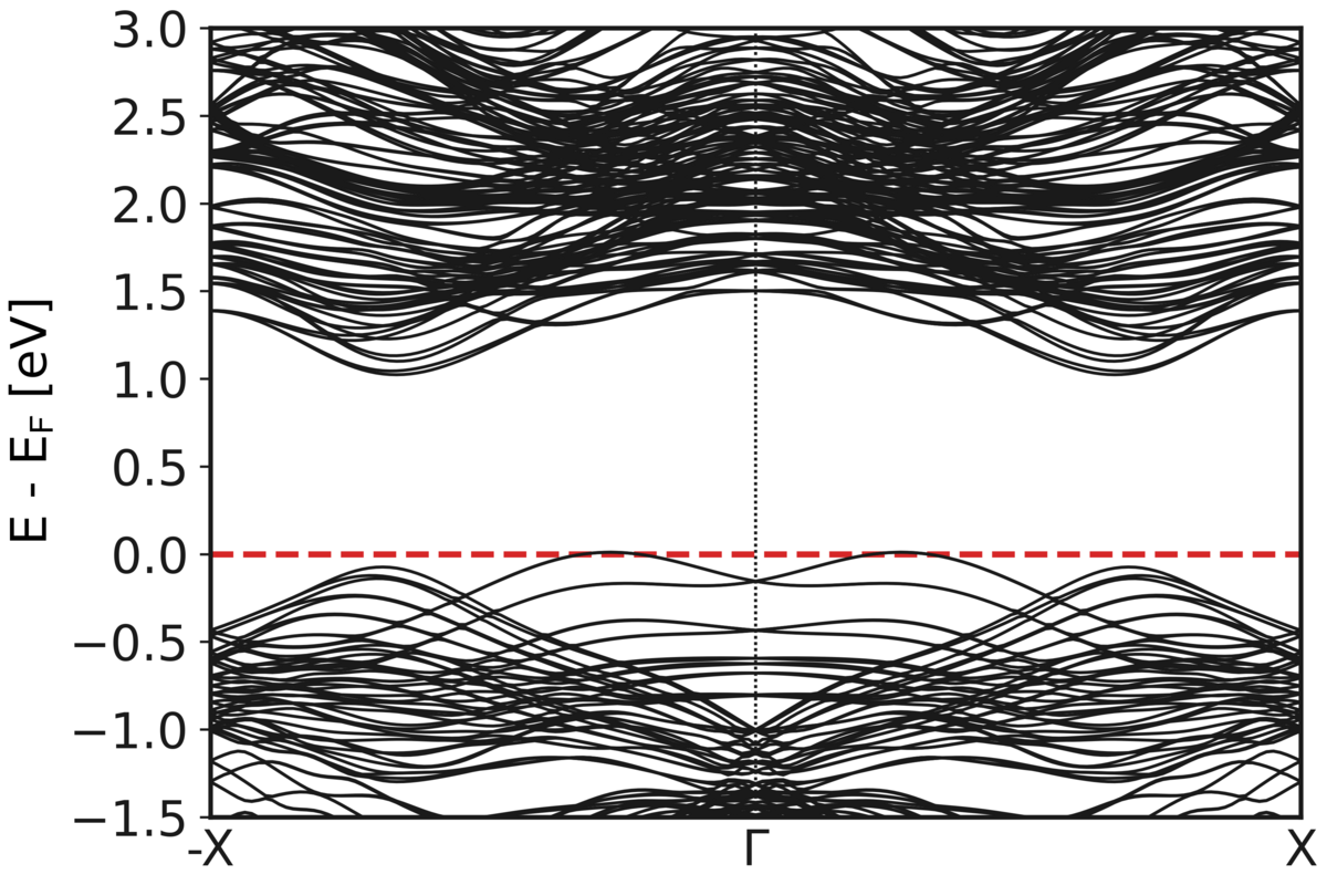
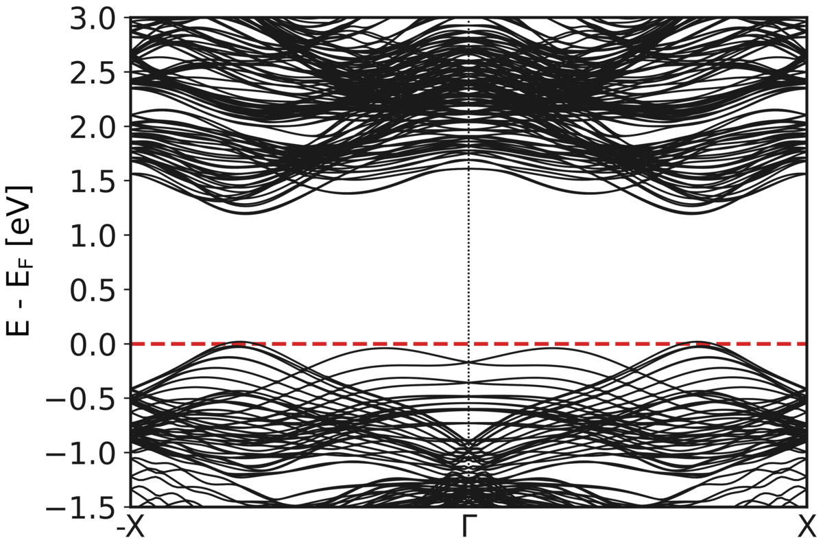
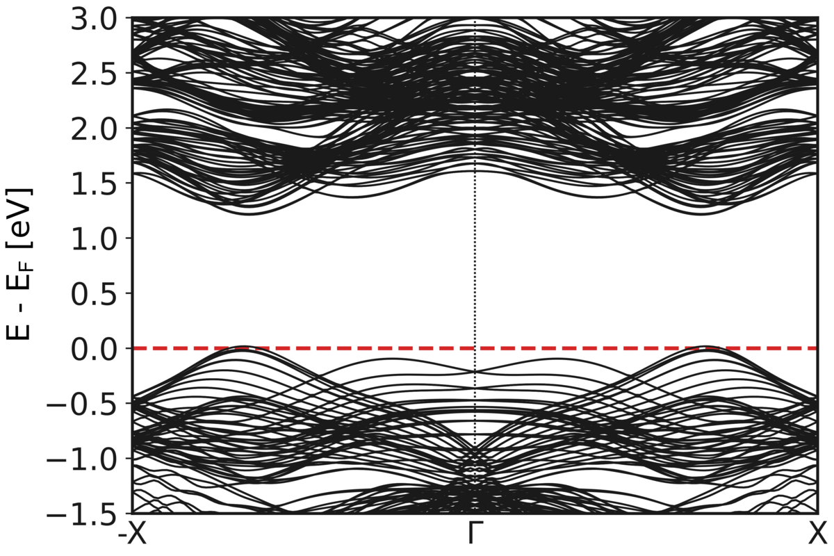
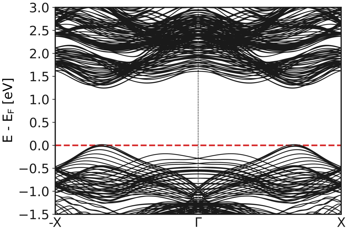
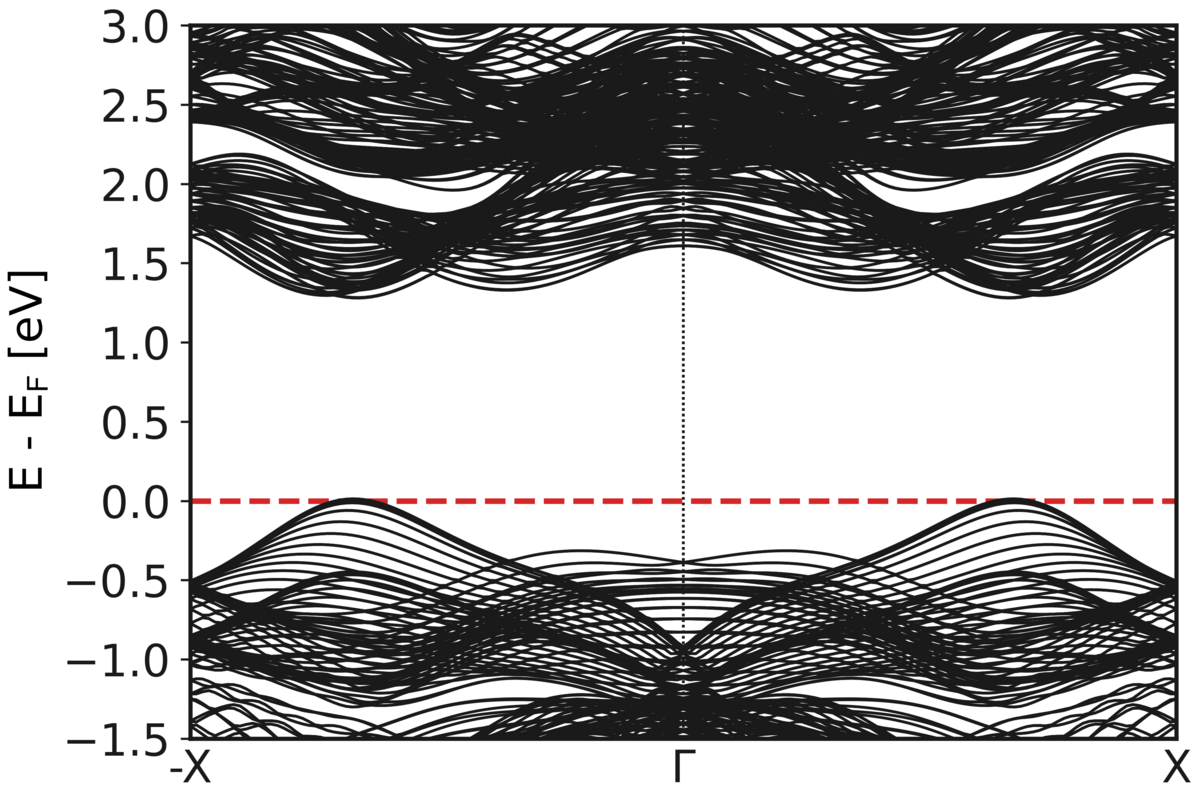
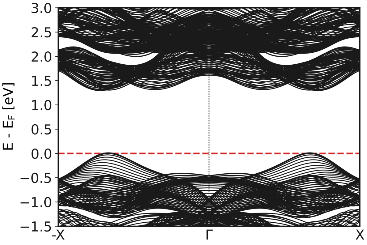
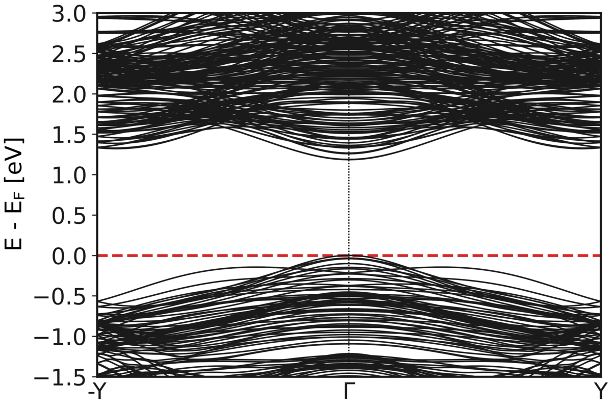
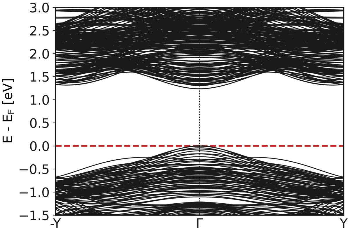
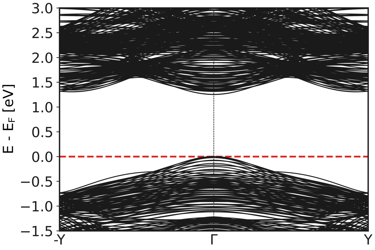
The relaxation in the wrinkles leads to differences in the electronic structure compared to the nanotube-like structures used for the initial geometry. Yet, the comparison of the band dispersion for NTs and wrinkles with approximately the same average curvature (especially for large wavelength or diameter) also reveals similarities especially for the conduction and valence band (CB and VB). Figure 3 shows the band structures for a (24,24) nanotube (d=44 ) and the corresponding wrinkle ().
Both the valence-band maximum (VBM) and conduction-band minimum (CBM) show large contributions from tungsten atoms (cf. Figure S3 for the monolayer in the rectangular unit cell) indicating that those are the high-symmetry points of the primitive unit cell which are mapped to the line (more details about the backfolding can be found in the SI [57], section “Brillouin zone of wrinkles/NTs and spin texture”). Not only the global band gap, , is comparable for this specific example but also the dispersion of the first few VBs and CBs and accordingly derived physical quantities such as mobility and conductivity. This is a promising outcome as it suggests that for global variables of large-scale wrinkles a similar nanotube can be used to reduce the computational cost. In Figure 4 we compare the direct band gap as function of the average curvature for all investigated systems.
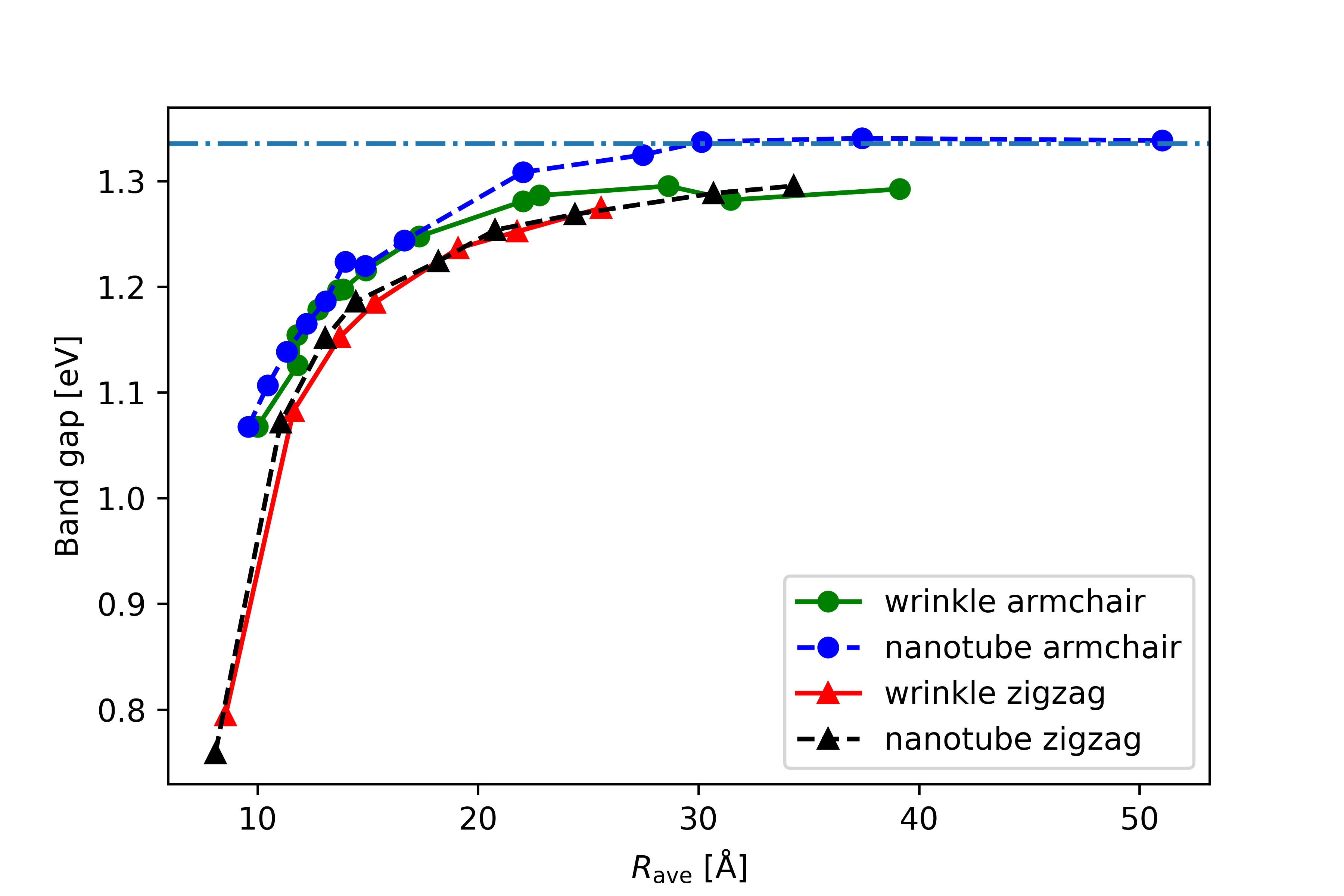
The global direct band gap of most wrinkles is slightly smaller than those of the NTs with similar average curvature and in both systems the band gap approaches the value of the monolayer, , for small average curvature, i.e., large radius of curvature – please note that the calculated band gap for the monolayer can vary depending on the settings[61]. Thus, NTs can possibly be used to model the global band gap changes in large wrinkles (or similar systems under inhomogeneous strain) if the average curvature of the wrinkles is taken into account. It is worth to reemphasize that the ab-initio modeling of inhomogeneous strain in wrinkles is computationally very demanding due to the symmetry breaking, the presence of many heavy atoms, and spin-orbit coupling and that this similarity can be utilized to simplify the theoretical modeling. One can then subsequently utilize helical boundary conditions to further reduce the computational cost. However, there are also some differences for the bands close to the VBM/CBM – in wrinkles we find more bands with similar dispersion but small differences in the maximum/minimum energy and this can explain the funneling found in wrinkled systems as explained in the following.
II.2 Funneling
Funneling is the phenomena of absorption and emission of light from different spatial positions along the wrinkle. The directional guiding of the excitons can be achieved by a spatial modification of, e.g., the dielectric screening[62] or the band gap of the material due to external strain.[37] This phenomena attracted the attention of numerous scientists, and was subject to several researches. [37, 38, 63, 39, 28, 30] It has for example been shown that the photovoltaic behavior of 2D materials [64] and light emitting diodes [65] can significantly be enhanced. Furthermore, it was proposed that highly directional exciton transport promises not only compelling advantages for exciton-based applications but that it could also be interesting for reaching truly 1D regimes to study quantum transport phenomena of correlated many-body states.[63] From the experimental point of view, photoluminescence microscopy is routinely used to study these systems although it can be quite challenging at the nanoscale; [38] other techniques such as time-resolved transient absorption microscopy[66] are possible too but also need additional input from theory to interpret the results. However, in conjunction with theoretical estimates of the band structure changes due to external strain[67, 68, 69] or different stacking regions[68, 70] a quantitative description of experimentally observed shifts of excitonic peaks is possible.
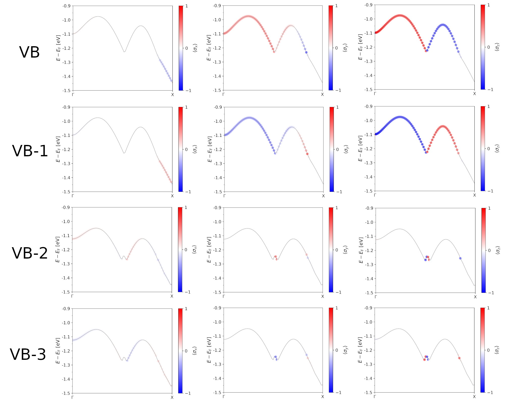
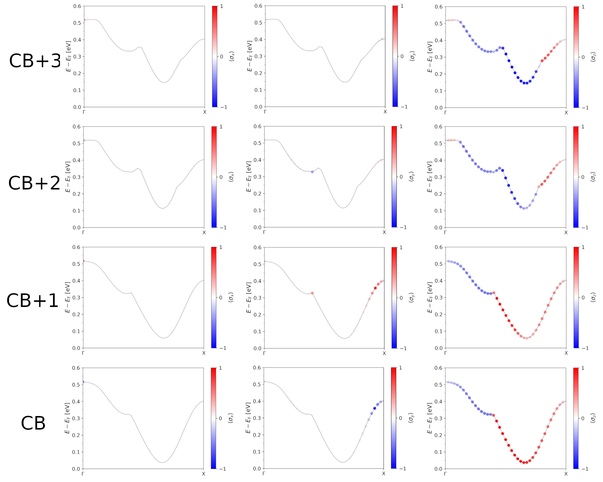
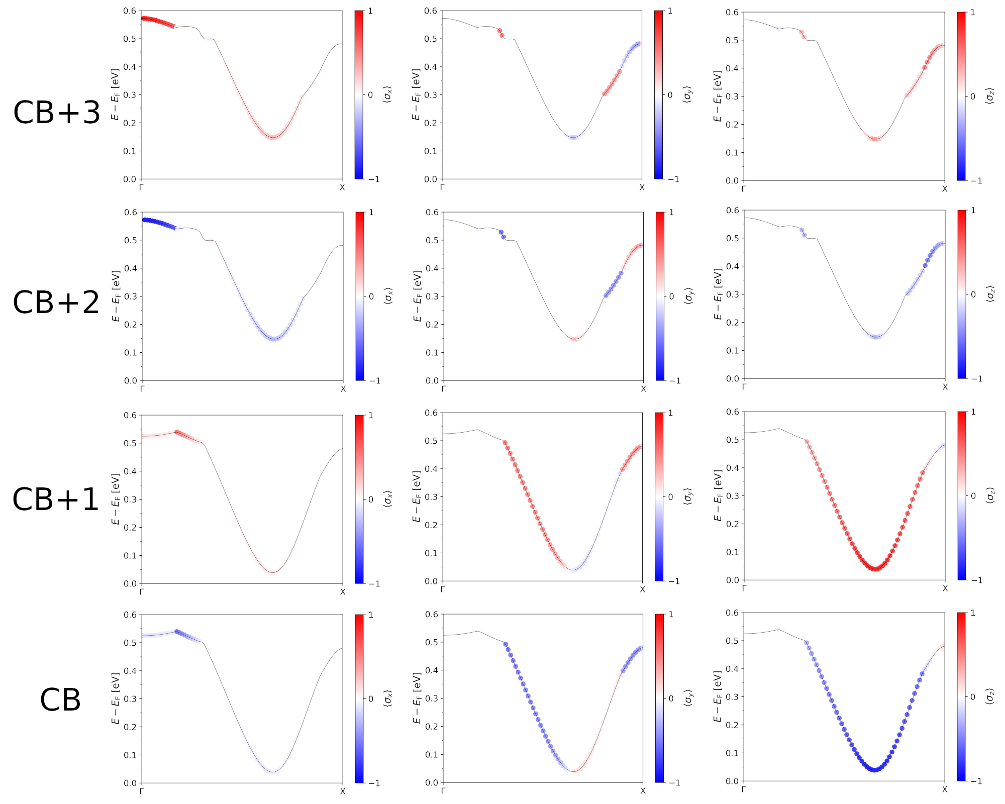
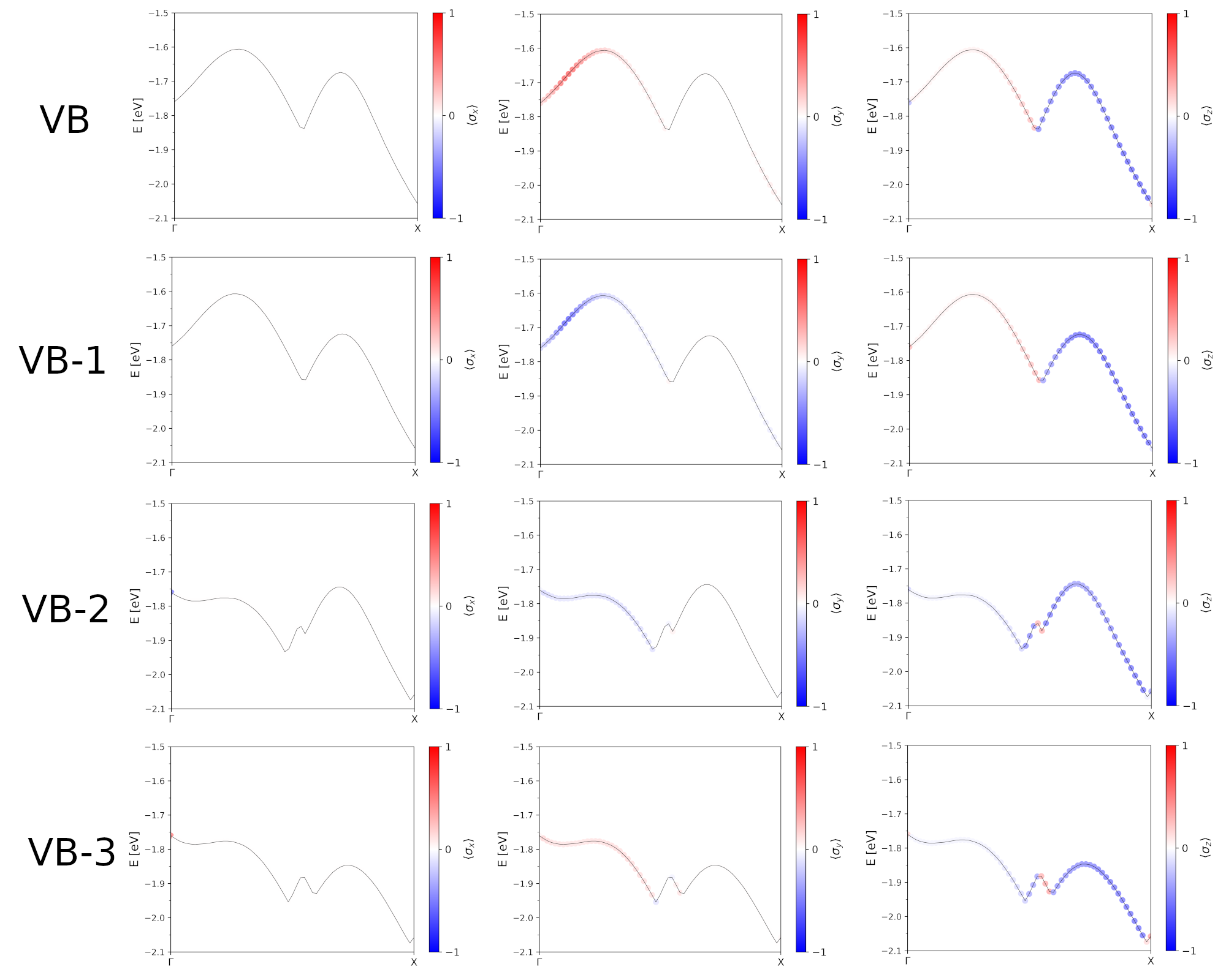
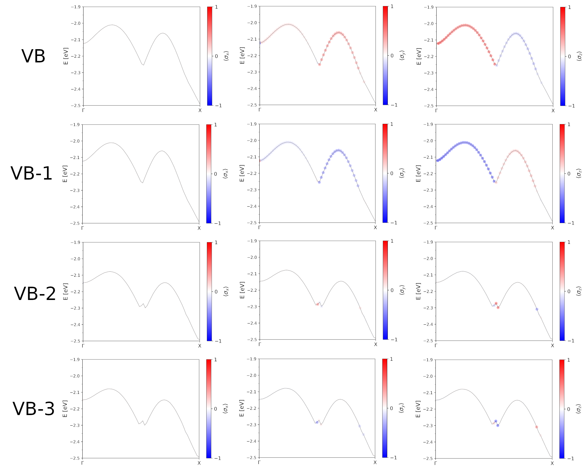
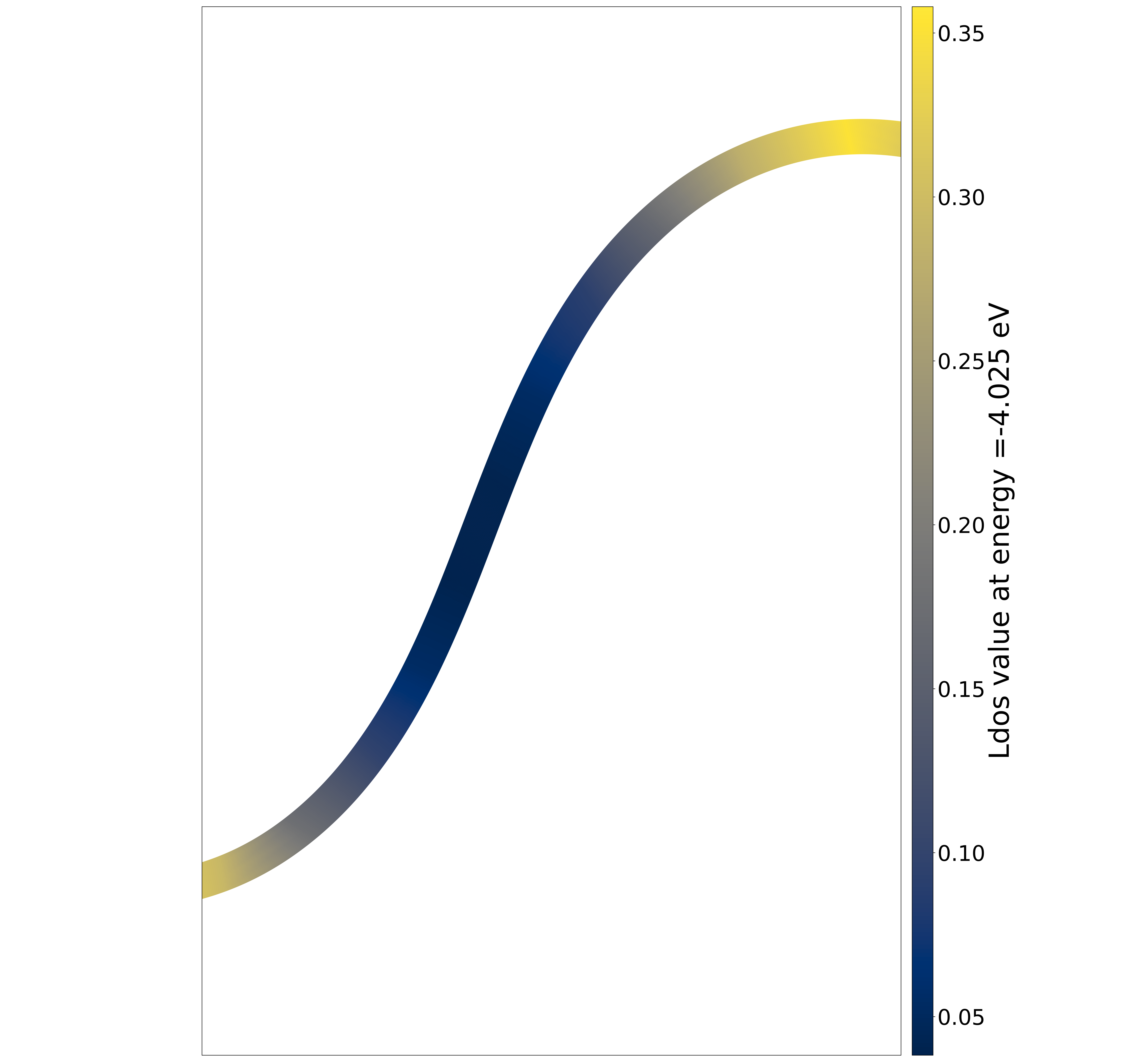
In order to understand the difference between all the bands close to the VBM and CBM and relate this to experimental observations, we projected the band structure on different atoms along the wrinkle. Figure 5 shows that the VBM is spread all over the wrinkle while the VB-1 and VB-2 (the two bands below the VB) close to the VBM are more localized in the straight and the curved region, respectively. The CBM on the other hand is localized at the top of the wrinkle in the regions with large local strain while the higher CB also show contributions from the straight regions. Since the different minima of the CBs have a larger difference in energy than the VBs, the lowest band gap is found in the regions with large local curvature. Figures S14a and S14b in the SI [57] show the variation of the local density of states (LDOS) along the (24,24) wrinkle close to VBM and CBM, respectively, and confirm that the energy levels close to the band gap are more localized close to the peaks and valleys of the wrinkle. Yet, since the band extrema also have small differences in the momentum direction which complicate the situation, further studies using, e.g., the Bethe-Salpeter equation to describe the excitonic states are needed which are – at the moment – however only possible for the smallest systems of our study.[71] Nevertheless, as shown previously, the changes of the local band gap give a very good estimate of the shifts of excitonic peaks.[67, 68, 69]
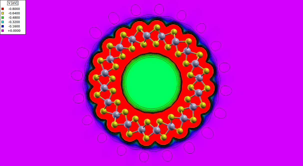
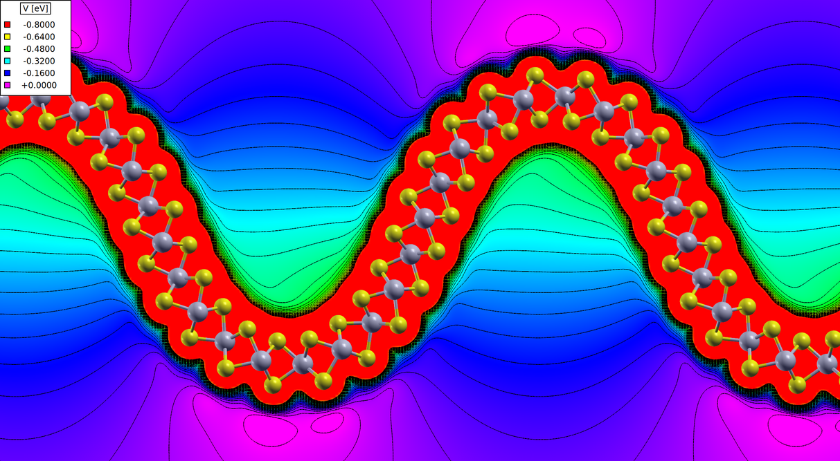
Another important effect which will influence the dynamics of excitons, are the internal electric fields which are induced by the curvature [72]. In order to estimate the local electric field which result from the local curvature, we use the dipoles as calculated with the Hirshfeld partitioning scheme [73]. Figure 6 shows the magnitude and direction of the tungsten dipoles for the (24,24) wrinkle. One can clearly see that the dipoles at the peaks and valleys of the wrinkle are larger – due to this inhomogeneity there will be an effective electric field which could be another force driving the excitons to the regions with higher curvature. This inhomogeneity can also be seen in the contour plot of the total electrostatic potential, Figure S13. Yet, in experiments the screening by a substrate might be important as well and we will leave this fascinating topic for future work since this is beyond the current investigation.

Most interestingly, the internal electric field due to the dipoles leads to a Rashba-like SOC splitting as can be seen in Figures 3 and S15 for the CB states crossing at the point.
II.3 SOC splitting
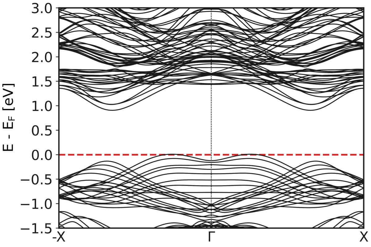
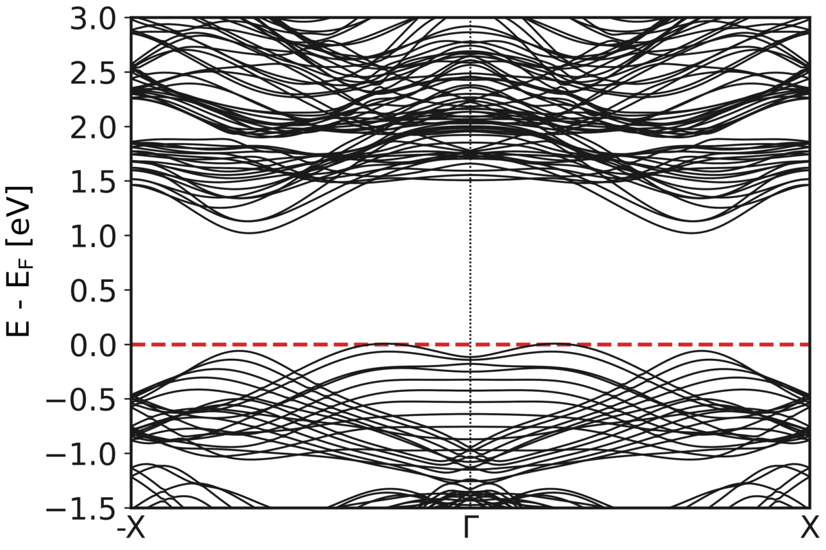
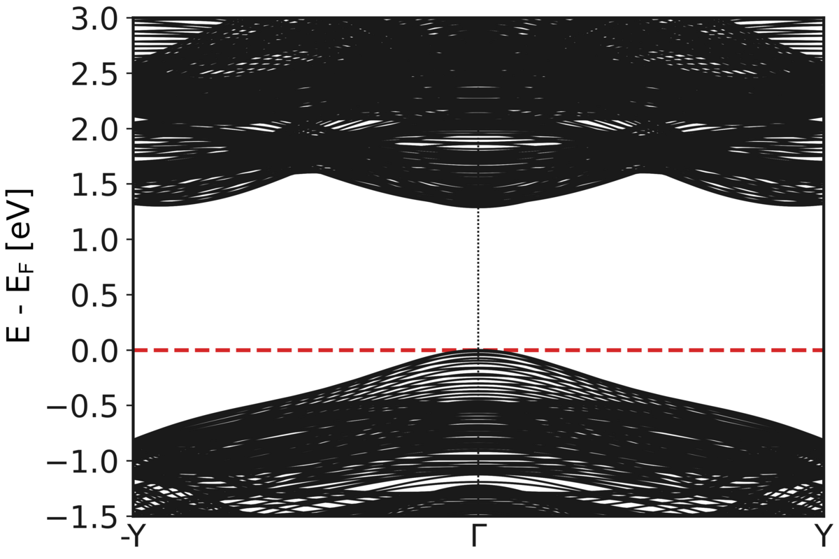
The splitting of the bands close to the point resembles the Rashba spin-orbit splitting found in quantum wells or Janus-type TMDCs [74, 75]. Comparing band structures with and without SOC (shown in the SI [57], Figure S16), we can directly see the effect of SOC on the band dispersion. We observed this Rashba-like splitting (i.e., splitting of the band energies in momentum direction [49]) in all investigated systems and furthermore found in very small NTs an apparent avoided crossing of the SOC-split states which might be either due to the interaction between atoms of opposite sides or an artifact due to possible strain-induced changes of the hexagonal symmetry (cf., Figures 7 and S7).
The Rashba splitting in nanoscale wrinkles and NTs occurs due to the symmetry breaking caused by the inhomogenous strain field and the resulting electric dipoles perpendicular to the wrinkle and nanotube. Hence, in presence of spin-orbit coupling two degenerate spin bands split into two separate bands in momentum direction. These SOC-split states are mainly localized at the top (i.e., highest curvature part) of the wrinkle (cf., Figure 5).
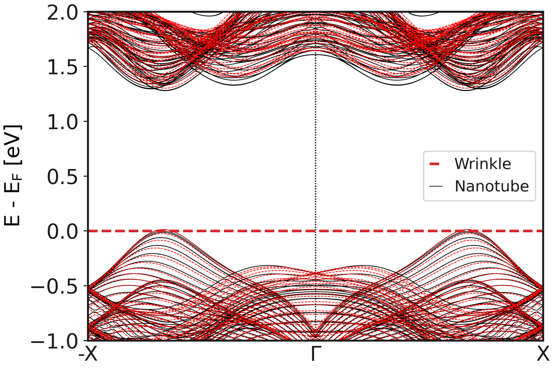
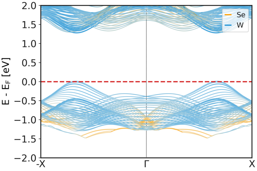
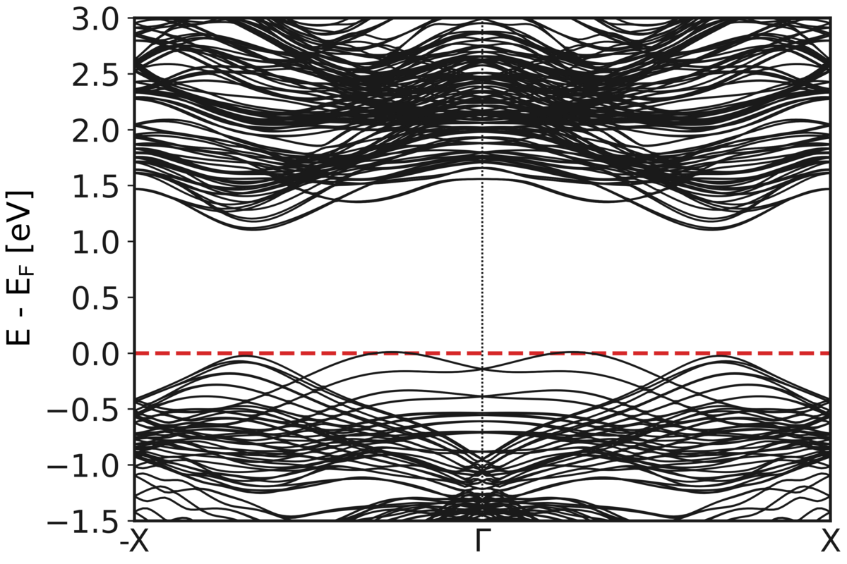
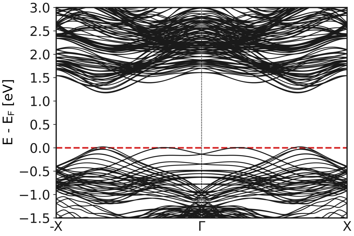
Figure 7 depicts the band structure of the armchair (11,11) wrinkle and nanotube highlighting also the changes with increasing curvature if compared to Figure 3 – the splitting not only increases in momentum direction but the Rashba-split states also move up in energy such that they eventually become the VBM (see also the Figures S17–S20). One main difference of the wrinkle with respect to the nanotube is the larger splitting between the uppermost VBs and the lower bands which might be due to the higher curvature at the top of the wrinkles and the more diverse local strain state in wrinkles.
Another important difference can be found in the spin texture of the highest valence bands and lowest conduction bands as shown in the section “Brillouin zone of wrinkles/NTs and spin texture” in the SI [57]. While the NTs always show twofold degenerate bands coming from the K and K’ point of the 2D material, the degeneracy is slightly lifted in the wrinkle probably due to the different strain states along one period of the wrinkle – in fact, a slight asymmetry is also visible in the contour plot of the total electrostatic potential shown in Figure S13. This also leads to a different spin texture (compared to the NT) in which the VB of the wrinkle does not automatically have the opposite spin expectation value of the band just below (VB-1). The largest contribution of for the Rashba-split states close to is always coming from and , i.e., the directions perpendicular to . Figures S5 and S7 furthermore show that for the wrinkle the lowest CB has the opposite spin polarization of the VB at the K point (the extrema closer to the X point); the inhomogeneous strain is not large enough to change the pattern which is also observed in the monolayer.[76]
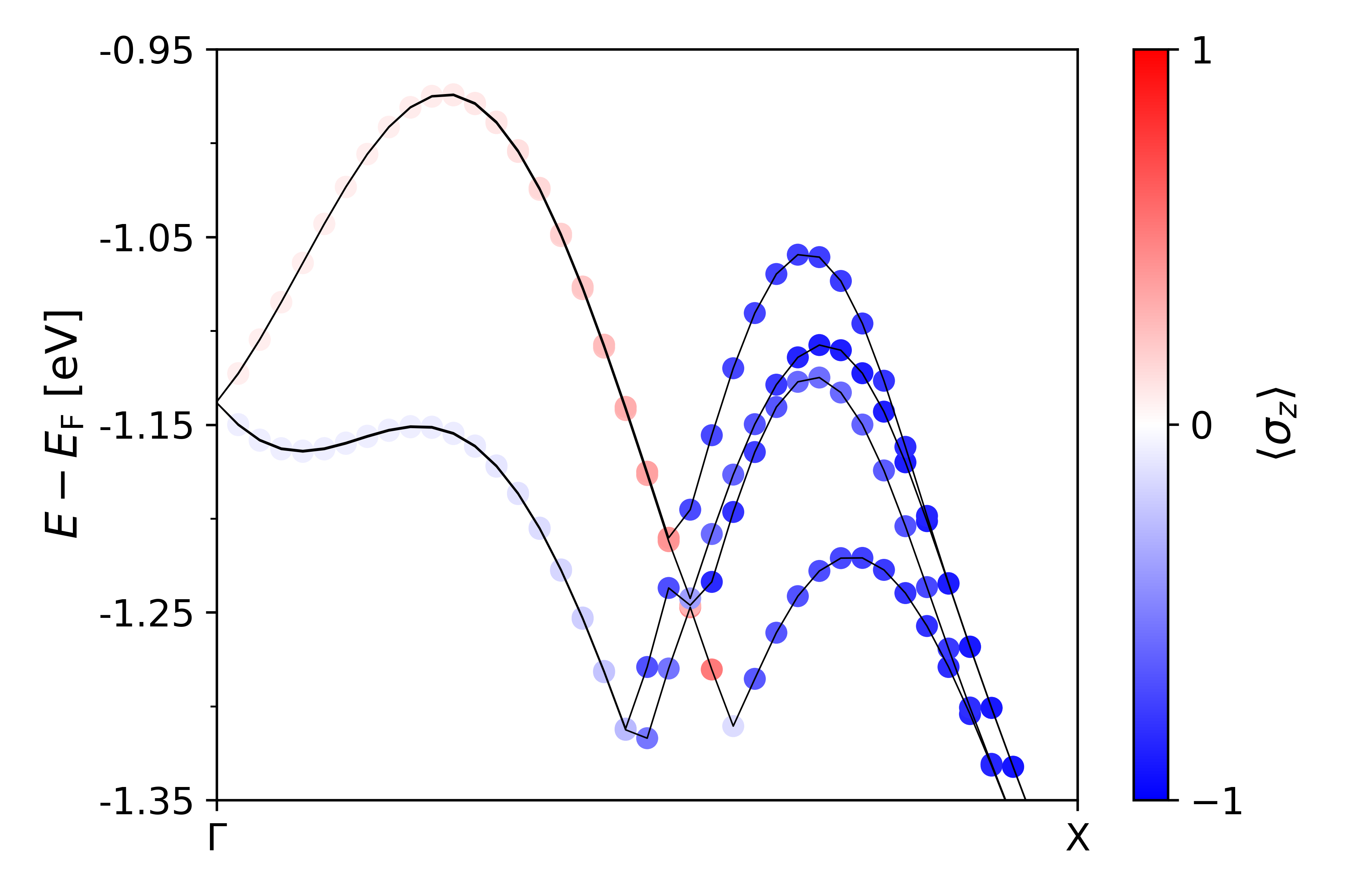
Figure 8 depicts the expectation value for the four highest valence bands of the (11,11) wrinkle. Note that close to only two bands are visible since the bands are doubly-degenerate due to the folding to the 1D Brillouin zone. We thus show the average expectation value of the two degenerate states . The expectation values and are either zero or the two degenerate states have opposite signs. A complete discussion about the individual spin states can be found in the SI [57], Figures. S5–S8.
In order to examine the strength of the Rashba-like splitting the Rashba coupling parameter[77], , has been calculated for the armchair systems using
| (2) |
where and are the Rashba energy and the shift of the bands in the momentum direction, respectively. Unfortunately, the different back folding of the bands in the zigzag structures leads to the primitive unit cell’s point being mapped to thus obscuring the SOC-split states. This prevents an easy and correct fitting of the Rashba model to the band structure even if the band structures in the SI [57] clearly show the same splitting.
The Rashba coupling parameter shown in Figure 9 decreases as the wrinkle wavelength or nanotube diameter increases. This trend can be explained by the decreasing strain difference between the outer and the inner chalcogen layer and the corresponding smaller induced electric field. It is also evident that band gap and band dispersion of large NTs and wrinkles are converging to the corresponding flat monolayer (cf. Figures S3 and S19). Furthermore, the Rashba coupling parameter is only comparable between wrinkles and NTs if it is shown with respect to the minimum radius of curvature, , i.e. the highest curvature. This is once more due to the wrinkles having higher curvature at their peaks. The Rashba coupling parameter in our structures are relatively high and almost half the size of elemental surfaces [78] and one order of magnitude larger than in Janus type TMDCs [53, 79].
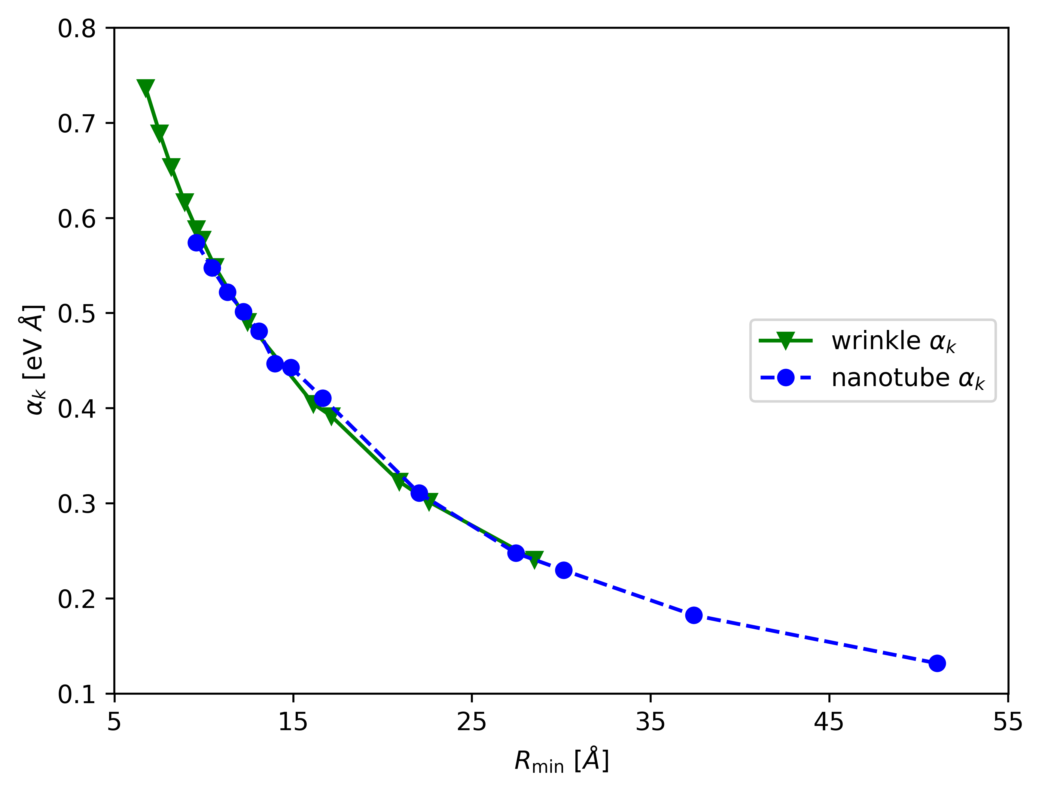
Furthermore, the coupling parameter in wrinkles/NTs with small can also be comparable to the one found in heterostructures including \ceBiSb[80] even if one probably needs to include higher order terms to properly describe the large splitting.[81] It should be noted that the largest splittings are those easiest to reach experimentally since the bands move above the monolayer VBM at . This is also a possibility for tuning the electronic structure and the SOC-induced splitting for the application in spintronic devices: using (mono-)layers of TMDCs deposited on elastic substrates which can be used to induce different wrinkle morphologies as shown in, e.g., Refs. 82, 83.
It should be noted however that the exact shape of the wrinkle can be different from our research, e.g., due to substrate effects; the conclusions in above sections still hold as they are due to strain effects and the subsequent symmetry breaking. Yet slight quantitative differences are expected and require further investigations. We expect that nanotubes can still be used to model the curvature effects in wrinkled systems and that the variation of the local band gap leads to exciton funneling. Furthermore, the interaction with substrates and additional external fields might lead to even higher Rashba-like splittings.
III Conclusion
We investigated NTs and 2D wrinkles of \ceWSe2 theoretically and analyzed the influence of the induced inhomogeneous strain on their electronic properties but the following conclusions should generally apply to all TMDCs. We found that the inhomogeneous strain causes symmetry breaking in these structures which leads to a Rashba-like splitting of the valence band at . Therefore, these structures – particularly the smaller wavelengths – could be promising candidates for spintronic applications. In fact, spin-polarized STM using an additional graphene layer as electrode[84, 85] should be able to measure the Rashba-like splitting of the VBM. We believe that this is a general feature of wrinkled 2D TMDCs due to the non-uniform strain and our study will thus pave the way for the employment of a wide range of materials in spintronic devices. This bears witness to the important role of SOC in the physics of 2D TMDCs nanoscale wrinkles and NTs. Moreover, wrinkling should be regarded as a method for introducing out of plane dipoles in the 2D system which might be useful in other contexts. Investigations of bilayers and hetrostructures made of dichalcogenides could even result in appearance of more fascinating phenomena.
Furthermore, nanoscale TMDC wrinkles do not follow a sine wave profile as suggested by continuum mechanics and which has been widely utilized in strain analysis. The profiles in our study are basically composed of a superposition of two sine waves. Thus, the curvature varies smoother in the profiles maxima and minima. This suggests that the classical formulation of such structures conceals important physical properties and conclusions based upon might be misleading, e.g., in the calculation of strain fields from the surface topology in nanoscale wrinkles. Moreover, we attribute the funneling of excitons to the localization of states in different spatial locations due to the presence of the inhomogeneous strain. Yet, more advanced calculations are needed to evaluate the influence of the, e.g., induced dipoles or substrate and an additional investigation of the wrinkled samples via STM [84, 85] could furthermore help to understand the band alignment better.
Additionally, we demonstrated that NTs can be used to approximate the wrinkles for reduction of computational costs, nonetheless one needs to take care of the differences that exist.
IV Methods
NTs and wrinkles of a monolayer of \ceWSe2 having two edge types: armchair and zigzag were investigated using an all-electron method based on DFT as implemented in FHI-aims code [86]. We utilized the Perdew–Burke–Ernzerhof (PBE) exchange-correlation functional [87] together with the Tkatchenko-Scheffler dispersion correction [88] and the non-self-consistent SOC implementation [89]. Additionally, no symmetry was imposed on any of the structures in this calculations. In order to compare wrinkles and NTs, the initial wrinkled structure was created with an elliptical profile as shown in Figure 1 with a wavelength to amplitude ratio of and using NTs as input. The unit cell was fixed only in the direction of the wrinkles with to retain the compression. All structures have been relaxed utilizing the Broyden-Fletcher-Godfarb-Shanno method to reach forces below . Subsequently, the Mulliken projected band structures with and without spin-orbit coupling were calculated. NTs are labeled with the rolling vector (m,n) and for wrinkles the similar notation is used such that the (m,n) wrinkle is similar to the (m,n) nanotube. The geometries as well as the band structures for all systems which have been investigated within this work were uploaded to the NOMAD repository, Ref. 90
Conflicts of interest
There are no conflicts of interest to declare.
Acknowledgements.
The authors would like to thank Prof. T. Heine, Dr. A. Kuc, R. Kempt and F. Arnold for fruitful discussions. This project was financially supported by the SFB 1415, Project ID No. 417590517. We would like to acknowledge the Center for Information Service and High Performance Computing [Zentrum für Informationsdienste und Hochleistungsrechnen (ZIH)] at TU Dresden. Also, the authors gratefully acknowledge the Gauss Centre for Supercomputing e.V. (www.gauss-centre.eu) for funding this project by providing computing time through the John von Neumann Institute for Computing (NIC) on the GCS Supercomputer JUWELS [91] at Jülich Supercomputing Centre (JSC).Table of Contents
References
References
- Novoselov et al. [2004] K. S. Novoselov, A. K. Geim, S. V. Morozov, D.-e. Jiang, Y. Zhang, S. V. Dubonos, I. V. Grigorieva, and A. A. Firsov, Electric field effect in atomically thin carbon films, science 306, 666 (2004).
- Song et al. [2010] L. Song, L. Ci, H. Lu, P. B. Sorokin, C. Jin, J. Ni, A. G. Kvashnin, D. G. Kvashnin, J. Lou, B. I. Yakobson, et al., Large scale growth and characterization of atomic hexagonal boron nitride layers, Nano letters 10, 3209 (2010).
- Ayari et al. [2007] A. Ayari, E. Cobas, O. Ogundadegbe, and M. S. Fuhrer, Realization and electrical characterization of ultrathin crystals of layered transition-metal dichalcogenides, Journal of applied physics 101, 014507 (2007).
- Kuc et al. [2011] A. Kuc, N. Zibouche, and T. Heine, Influence of quantum confinement on the electronic structure of the transition metal sulfide t s 2, Physical Review B 83, 245213 (2011).
- Lorenz et al. [2014] T. Lorenz, M. Ghorbani-Asl, J.-O. Joswig, T. Heine, and G. Seifert, Is mos2 a robust material for 2d electronics?, Nanotechnology 25, 445201 (2014).
- Xu et al. [2021] H. Xu, J. Zhu, Q. Ma, J. Ma, H. Bai, L. Chen, and S. Mu, Two-dimensional mos2: structural properties, synthesis methods, and regulation strategies toward oxygen reduction, Micromachines 12, 240 (2021).
- Woomer et al. [2015] A. H. Woomer, T. W. Farnsworth, J. Hu, R. A. Wells, C. L. Donley, and S. C. Warren, Phosphorene: synthesis, scale-up, and quantitative optical spectroscopy, ACS nano 9, 8869 (2015).
- Miró et al. [2014] P. Miró, M. Audiffred, and T. Heine, An atlas of two-dimensional materials, Chemical Society Reviews 43, 6537 (2014).
- Ghorbani-Asl et al. [2016] M. Ghorbani-Asl, A. Kuc, P. Miro, and T. Heine, A single-material logical junction based on 2d crystal pds2, Advanced Materials 28, 853 (2016).
- Akinwande et al. [2017] D. Akinwande, C. J. Brennan, J. S. Bunch, P. Egberts, J. R. Felts, H. Gao, R. Huang, J.-S. Kim, T. Li, Y. Li, et al., A review on mechanics and mechanical properties of 2d materials—graphene and beyond, Extreme Mechanics Letters 13, 42 (2017).
- Brumme et al. [2015] T. Brumme, M. Calandra, and F. Mauri, First-principles theory of field-effect doping in transition-metal dichalcogenides: Structural properties, electronic structure, hall coefficient, and electrical conductivity, Physical Review B 91, 155436 (2015).
- Dai et al. [2019] Z. Dai, L. Liu, and Z. Zhang, Strain engineering of 2d materials: issues and opportunities at the interface, Advanced Materials 31, 1805417 (2019).
- Hong et al. [2017] Y. K. Hong, N. Liu, D. Yin, S. Hong, D. H. Kim, S. Kim, W. Choi, and Y. Yoon, Recent progress in high-mobility thin-film transistors based on multilayer 2d materials, Journal of Physics D: Applied Physics 50, 164001 (2017).
- Falin et al. [2021] A. Falin, M. Holwill, H. Lv, W. Gan, J. Cheng, R. Zhang, D. Qian, M. R. Barnett, E. J. Santos, K. S. Novoselov, et al., Mechanical properties of atomically thin tungsten dichalcogenides: Ws2, wse2, and wte2, ACS nano 15, 2600 (2021).
- Ahn [2020] E. C. Ahn, 2d materials for spintronic devices, npj 2D Materials and Applications 4, 1 (2020).
- Lu et al. [2020] Z. Lu, G. P. Neupane, G. Jia, H. Zhao, D. Qi, Y. Du, Y. Lu, and Z. Yin, 2d materials based on main group element compounds: phases, synthesis, characterization, and applications, Advanced Functional Materials 30, 2001127 (2020).
- Li et al. [2021] Z. Li, N. H. Attanayake, J. L. Blackburn, and E. M. Miller, Carbon dioxide and nitrogen reduction reactions using 2d transition metal dichalcogenide (tmdc) and carbide/nitride (mxene) catalysts, Energy & Environmental Science 14, 6242 (2021).
- Anju and Mohanan [2020] S. Anju and P. Mohanan, Biomedical applications of transition metal dichalcogenides (tmdcs), Synthetic Metals , 116610 (2020).
- Lin et al. [2021] Y.-C. Lin, R. Torsi, D. B. Geohegan, J. A. Robinson, and K. Xiao, Controllable thin-film approaches for doping and alloying transition metal dichalcogenides monolayers, Advanced Science 8, 2004249 (2021).
- Ghorbani-Asl et al. [2022] M. Ghorbani-Asl, S. Kretschmer, and A. V. Krasheninnikov, Two-dimensional materials under ion irradiation: from defect production to structure and property engineering, in Defects in Two-Dimensional Materials (Elsevier, 2022) pp. 259–301.
- Ma et al. [2021] Q. Ma, G. Ren, K. Xu, and J. Z. Ou, Tunable optical properties of 2d materials and their applications, Advanced Optical Materials 9, 2001313 (2021).
- Daghigh Shirazi et al. [2021] H. Daghigh Shirazi, Y. Dong, J. Niskanen, C. Fedele, A. Priimagi, V. P. Jokinen, and J. Vapaavuori, Multiscale hierarchical surface patterns by coupling optical patterning and thermal shrinkage, ACS applied materials & interfaces 13, 15563 (2021).
- Du et al. [2021] J. Du, H. Yu, B. Liu, M. Hong, Q. Liao, Z. Zhang, and Y. Zhang, Strain engineering in 2d material-based flexible optoelectronics, Small Methods 5, 2000919 (2021).
- Plechinger et al. [2015] G. Plechinger, A. Castellanos-Gomez, M. Buscema, H. S. Van Der Zant, G. A. Steele, A. Kuc, T. Heine, C. Schueller, and T. Korn, Control of biaxial strain in single-layer molybdenite using local thermal expansion of the substrate, 2D Materials 2, 015006 (2015).
- Ghorbani-Asl et al. [2013a] M. Ghorbani-Asl, N. Zibouche, M. Wahiduzzaman, A. F. Oliveira, A. Kuc, and T. Heine, Electromechanics in mos 2 and ws 2: nanotubes vs. monolayers, Scientific reports 3, 1 (2013a).
- Ghorbani-Asl et al. [2013b] M. Ghorbani-Asl, S. Borini, A. Kuc, and T. Heine, Strain-dependent modulation of conductivity in single-layer transition-metal dichalcogenides, Physical Review B 87, 235434 (2013b).
- Heine [2015] T. Heine, Transition metal chalcogenides: ultrathin inorganic materials with tunable electronic properties, Accounts of chemical research 48, 65 (2015).
- Peng et al. [2020] Z. Peng, X. Chen, Y. Fan, D. J. Srolovitz, and D. Lei, Strain engineering of 2d semiconductors and graphene: from strain fields to band-structure tuning and photonic applications, Light: Science & Applications 9, 190 (2020).
- Jiang et al. [2020] H. Jiang, L. Zheng, Z. Liu, and X. Wang, Two-dimensional materials: From mechanical properties to flexible mechanical sensors, InfoMat 2, 1077 (2020), https://onlinelibrary.wiley.com/doi/pdf/10.1002/inf2.12072 .
- Di Giorgio et al. [2022] C. Di Giorgio, E. Blundo, G. Pettinari, M. Felici, F. Bobba, and A. Polimeni, Mechanical, elastic, and adhesive properties of two-dimensional materials: From straining techniques to state-of-the-art local probe measurements, Advanced Materials Interfaces 9, 2102220 (2022), https://onlinelibrary.wiley.com/doi/pdf/10.1002/admi.202102220 .
- Haastrup et al. [2018] S. Haastrup, M. Strange, M. Pandey, T. Deilmann, P. S. Schmidt, N. F. Hinsche, M. N. Gjerding, D. Torelli, P. M. Larsen, A. C. Riis-Jensen, et al., The computational 2d materials database: high-throughput modeling and discovery of atomically thin crystals, 2D Materials 5, 042002 (2018).
- Roldán et al. [2015] R. Roldán, A. Castellanos-Gomez, E. Cappelluti, and F. Guinea, Strain engineering in semiconducting two-dimensional crystals, Journal of Physics: Condensed Matter 27, 313201 (2015).
- Lee et al. [2022a] G. Lee, M. Zarei, Q. Wei, Y. Zhu, and S. G. Lee, Surface wrinkling for flexible and stretchable sensors, Small 18, 2203491 (2022a).
- Schweikart and Fery [2009] A. Schweikart and A. Fery, Controlled wrinkling as a novel method for the fabrication of patterned surfaces, Microchimica Acta 165, 249 (2009).
- Knapp et al. [2021] A. Knapp, L. J. Nebel, M. Nitschke, O. Sander, and A. Fery, Controlling line defects in wrinkling: a pathway towards hierarchical wrinkling structures, Soft Matter 17, 5384 (2021).
- Yu et al. [2019] Y. Yu, C. Ng, T. A. König, and A. Fery, Tackling the scalability challenge in plasmonics by wrinkle-assisted colloidal self-assembly, Langmuir 35, 8629 (2019).
- Lee et al. [2020] J. Lee, S. J. Yun, C. Seo, K. Cho, T. S. Kim, G. H. An, K. Kang, H. S. Lee, and J. Kim, Switchable, tunable, and directable exciton funneling in periodically wrinkled ws2, Nano Letters 21, 43 (2020).
- Koo et al. [2021a] Y. Koo, Y. Kim, S. H. Choi, H. Lee, J. Choi, D. Y. Lee, M. Kang, H. S. Lee, K. K. Kim, G. Lee, et al., Tip-induced nano-engineering of strain, bandgap, and exciton funneling in 2d semiconductors, Advanced Materials 33, 2008234 (2021a).
- Shao et al. [2022] J. Shao, F. Chen, W. Su, N. Kumar, Y. Zeng, L. Wu, and H.-W. Lu, Probing nanoscale exciton funneling at wrinkles of twisted bilayer mos2 using tip-enhanced photoluminescence microscopy, The Journal of Physical Chemistry Letters 13, 3304 (2022).
- Jiang and Pachter [2022a] J. Jiang and R. Pachter, Analysis of localized excitons in strained monolayer wse 2 by first principles calculations, Nanoscale (2022a).
- Parto et al. [2021] K. Parto, S. I. Azzam, K. Banerjee, and G. Moody, Defect and strain engineering of monolayer wse2 enables site-controlled single-photon emission up to 150 k, Nature communications 12, 1 (2021).
- Wang et al. [2021a] Q. Wang, J. Maisch, F. Tang, D. Zhao, S. Yang, R. Joos, S. L. Portalupi, P. Michler, and J. H. Smet, Highly polarized single photons from strain-induced quasi-1d localized excitons in wse2, Nano letters 21, 7175 (2021a).
- Tenne et al. [1992] R. Tenne, L. Margulis, M. e. Genut, and G. Hodes, Polyhedral and cylindrical structures of tungsten disulphide, Nature 360, 444 (1992).
- Sinha et al. [2021] S. S. Sinha, L. Yadgarov, S. B. Aliev, Y. Feldman, I. Pinkas, P. Chithaiah, S. Ghosh, A. Idelevich, A. Zak, and R. Tenne, Mos2 and ws2 nanotubes: Synthesis, structural elucidation, and optical characterization, The Journal of Physical Chemistry C 125, 6324 (2021).
- Ghosh et al. [2019] S. Ghosh, A. S. Banerjee, and P. Suryanarayana, Symmetry-adapted real-space density functional theory for cylindrical geometries: Application to large group-iv nanotubes, Physical Review B 100, 125143 (2019).
- Nepal et al. [2019] N. K. Nepal, L. Yu, Q. Yan, and A. Ruzsinszky, First-principles study of mechanical and electronic properties of bent monolayer transition metal dichalcogenides, Physical Review Materials 3, 073601 (2019).
- Kumar and Suryanarayana [2020] S. Kumar and P. Suryanarayana, Bending moduli for forty-four select atomic monolayers from first principles, Nanotechnology 31, 43LT01 (2020).
- Safeer et al. [2020] C. Safeer, J. Ingla-Aynés, N. Ontoso, F. Herling, W. Yan, L. E. Hueso, and F. Casanova, Spin hall effect in bilayer graphene combined with an insulator up to room temperature, Nano Letters 20, 4573 (2020).
- Manchon et al. [2015] A. Manchon, H. C. Koo, J. Nitta, S. Frolov, and R. Duine, New perspectives for rashba spin–orbit coupling, Nature materials 14, 871 (2015).
- Zibouche et al. [2014] N. Zibouche, A. Kuc, J. Musfeldt, and T. Heine, Transition-metal dichalcogenides for spintronic applications, Annalen der Physik 526, 395 (2014).
- Klein et al. [2022] J. Klein, J. Wierzbowski, P. Soubelet, T. Brumme, L. Maschio, A. Kuc, K. Müller, A. V. Stier, and J. J. Finley, Electrical control of orbital and vibrational interlayer coupling in bi-and trilayer 2 h- mos 2, Physical Review Materials 6, 024002 (2022).
- Chen et al. [2021] J. Chen, K. Wu, W. Hu, and J. Yang, Spin–orbit coupling in 2d semiconductors: A theoretical perspective, The Journal of Physical Chemistry Letters 12, 12256 (2021).
- Cheng et al. [2013] Y. Cheng, Z. Zhu, M. Tahir, and U. Schwingenschlögl, Spin-orbit–induced spin splittings in polar transition metal dichalcogenide monolayers, EPL (Europhysics Letters) 102, 57001 (2013).
- Yao et al. [2017] Q.-F. Yao, J. Cai, W.-Y. Tong, S.-J. Gong, J.-Q. Wang, X. Wan, C.-G. Duan, and J. Chu, Manipulation of the large rashba spin splitting in polar two-dimensional transition-metal dichalcogenides, Physical review B 95, 165401 (2017).
- Izumida et al. [2009] W. Izumida, K. Sato, and R. Saito, Spin–orbit interaction in single wall carbon nanotubes: Symmetry adapted tight-binding calculation and effective model analysis, Journal of the Physical Society of Japan 78, 074707 (2009), https://doi.org/10.1143/JPSJ.78.074707 .
- Chico et al. [2009] L. Chico, M. P. López-Sancho, and M. C. Muñoz, Curvature-induced anisotropic spin-orbit splitting in carbon nanotubes, Phys. Rev. B 79, 235423 (2009).
- [57] See supplemental material at [url will be inserted by publisher] for a simple model for the curvature analysis, tables with the average/maximum curvature of all investigated systems, a band structure of the unstrained monolayer in the rectangular unit cell, a discussion of the brillouin zones of wrinkles/nanotubes including the spin expectation values for the 4 lowest/highest conduction/valence bands for the (11,11) systems and a brief discussion of the spin texture, contour plots of the total electrostatic potential for the (10,10) nanotube/wrinkle, the local density of states of the vbm/cbm along the (11,11) wrinkle, additional comparisons of the band structures of wrinkles and nanotubes, band structures projected onto specific regions of the wrinkles, and band structures near the fermi energy for all investigated systems and the additional references [92, 93, 94].
- Xie and Oshima [2021] L. Xie and Y. Oshima, Quantitative estimation of atom-scaled ripple structure using transmission electron microscopy images, Nanotechnology 32, 185703 (2021).
- Xie and Oshima [2022] L. Xie and Y. Oshima, Nonlinear mechanical response of rippled mos2 nanosheets evaluated by in situ transmission electron microscopy, Applied Surface Science , 153708 (2022).
- Wang et al. [2021b] J. Wang, M. Han, Q. Wang, Y. Ji, X. Zhang, R. Shi, Z. Wu, L. Zhang, A. Amini, L. Guo, et al., Strained epitaxy of monolayer transition metal dichalcogenides for wrinkle arrays, ACS nano 15, 6633 (2021b).
- Tran et al. [2022] T. N. Tran, M. T. Dang, Q. H. Tran, T. T. Luong, and V. A. Dinh, Band valley modification under strain in monolayer wse2, AIP Advances 12, 115023 (2022), https://doi.org/10.1063/5.0127204 .
- Peimyoo et al. [2020] N. Peimyoo, H.-Y. Wu, J. Escolar, A. De Sanctis, G. Prando, F. Vollmer, F. Withers, A. C. Riis-Jensen, M. F. Craciun, K. S. Thygesen, and S. Russo, Engineering dielectric screening for potential-well arrays of excitons in 2d materials, ACS Applied Materials & Interfaces 12, 55134 (2020), pMID: 33232104, https://doi.org/10.1021/acsami.0c14696 .
- Dirnberger et al. [2021] F. Dirnberger, J. D. Ziegler, P. E. F. Junior, R. Bushati, T. Taniguchi, K. Watanabe, J. Fabian, D. Bougeard, A. Chernikov, and V. M. Menon, Quasi-1d exciton channels in strain-engineered 2d materials, Science Advances 7, eabj3066 (2021), https://www.science.org/doi/pdf/10.1126/sciadv.abj3066 .
- Harats and Bolotin [2020] M. G. Harats and K. I. Bolotin, Limits of funneling efficiency in non-uniformly strained 2d semiconductors, 2D Materials 8, 015010 (2020).
- Jiang et al. [2021] Y. Jiang, J. Wei, and M. Yuan, Energy-funneling process in quasi-2d perovskite light-emitting diodes, The Journal of Physical Chemistry Letters 12, 2593 (2021).
- Yuan et al. [2020] L. Yuan, B. Zheng, J. Kunstmann, T. Brumme, A. B. Kuc, C. Ma, S. Deng, D. Blach, A. Pan, and L. Huang, Twist-angle-dependent interlayer exciton diffusion in ws2-wse2 heterobilayers, Nature Materials 19, 617 (2020).
- Koo et al. [2021b] Y. Koo, Y. Kim, S. H. Choi, H. Lee, J. Choi, D. Y. Lee, M. Kang, H. S. Lee, K. K. Kim, G. Lee, and K.-D. Park, Tip-induced nano-engineering of strain, bandgap, and exciton funneling in 2d semiconductors, Advanced Materials 33, 2008234 (2021b), https://onlinelibrary.wiley.com/doi/pdf/10.1002/adma.202008234 .
- Cho et al. [2021] C. Cho, J. Wong, A. Taqieddin, S. Biswas, N. R. Aluru, S. Nam, and H. A. Atwater, Highly strain-tunable interlayer excitons in mos2/wse2 heterobilayers, Nano Letters 21, 3956 (2021), pMID: 33914542, https://doi.org/10.1021/acs.nanolett.1c00724 .
- Koo et al. [2022] Y. Koo, H. Lee, T. Ivanova, A. Kefayati, V. Perebeinos, E. Khestanova, V. Kravtsov, and K.-D. Park, Dynamical control of interlayer excitons and trions in wse2/mo0.5w0.5se2 heterobilayer via tunable near-field cavity (2022).
- Yuan et al. [2023] L. Yuan, B. Zheng, Q. Zhao, R. Kempt, T. Brumme, A. B. Kuc, C. Ma, S. Deng, A. Pan, and L. Huang, Strong dipolar repulsion of one-dimensional interfacial excitons in monolayer lateral heterojunctions, ACS nano (2023).
- Jiang and Pachter [2022b] J. Jiang and R. Pachter, Analysis of localized excitons in strained monolayer wse2 by first principles calculations, Nanoscale 14, 11378 (2022b).
- Shi et al. [2018] W. Shi, Y. Guo, Z. Zhang, and W. Guo, Flexoelectricity in monolayer transition metal dichalcogenides, The journal of physical chemistry letters 9, 6841 (2018).
- Hirshfeld [1977] F. L. Hirshfeld, Bonded-atom fragments for describing molecular charge densities, Theoretica chimica acta 44, 129 (1977).
- Gan et al. [2022] Z. Gan, I. Paradisanos, A. Estrada-Real, J. Picker, E. Najafidehaghani, F. Davies, C. Neumann, C. Robert, P. Wiecha, K. Watanabe, et al., Chemical vapor deposition of high-optical-quality large-area monolayer janus transition metal dichalcogenides, Advanced Materials 34, 2205226 (2022).
- Yin et al. [2018] G. Yin, D. Zhu, D. Lv, A. Hashemi, Z. Fei, F. Lin, A. V. Krasheninnikov, Z. Zhang, H.-P. Komsa, and C. Jin, Hydrogen-assisted post-growth substitution of tellurium into molybdenum disulfide monolayers with tunable compositions, Nanotechnology 29, 145603 (2018).
- Zhang et al. [2015] X.-X. Zhang, Y. You, S. Y. F. Zhao, and T. F. Heinz, Experimental evidence for dark excitons in monolayer , Phys. Rev. Lett. 115, 257403 (2015).
- Kuc and Heine [2015] A. Kuc and T. Heine, The electronic structure calculations of two-dimensional transition-metal dichalcogenides in the presence of external electric and magnetic fields, Chemical Society Reviews 44, 2603 (2015).
- Bihlmayer et al. [2015] G. Bihlmayer, O. Rader, and R. Winkler, Focus on the rashba effect, New journal of physics 17, 050202 (2015).
- Liu et al. [2022] W. Liu, X. Li, C. Zhang, and S. Yan, Janus vxy monolayers with tunable large berry curvature, Journal of Semiconductors 43, 042501 (2022).
- Singh and Romero [2017] S. Singh and A. H. Romero, Giant tunable rashba spin splitting in a two-dimensional bisb monolayer and in bisb/aln heterostructures, Phys. Rev. B 95, 165444 (2017).
- Gupta and Yakobson [2021] S. Gupta and B. I. Yakobson, What dictates rashba splitting in 2d van der waals heterobilayers, Journal of the American Chemical Society 143, 3503 (2021), https://doi.org/10.1021/jacs.0c12809 .
- Giambastiani et al. [2022] D. Giambastiani, C. Tommasi, F. Bianco, F. Fabbri, C. Coletti, A. Tredicucci, A. Pitanti, and S. Roddaro, Strain-engineered wrinkles on graphene using polymeric actuators, Physical Review Applied 18, 024069 (2022).
- Lee et al. [2022b] H.-Y. Lee, G.-Z. Lu, J.-L. Shen, H.-Y. Lin, and Y.-F. Chen, Wrinkled 2d hybrid heterostructures for stretchable and sensitive photodetectors, Journal of Materials Chemistry C 10, 16370 (2022b).
- Qiu et al. [2021] Z. Qiu, M. Holwill, T. Olsen, P. Lyu, J. Li, H. Fang, H. Yang, M. Kashchenko, K. S. Novoselov, and J. Lu, Visualizing atomic structure and magnetism of 2d magnetic insulators via tunneling through graphene, Nature Communications 12, 70 (2021).
- Nieken et al. [2022] R. Nieken, A. Roche, F. Mahdikhanysarvejahany, T. Taniguchi, K. Watanabe, M. R. Koehler, D. G. Mandrus, J. Schaibley, and B. J. LeRoy, Direct stm measurements of r-type and h-type twisted mose2/wse2, APL Materials 10, 031107 (2022).
- Blum et al. [2009] V. Blum, R. Gehrke, F. Hanke, P. Havu, V. Havu, X. Ren, K. Reuter, and M. Scheffler, Ab initio molecular simulations with numeric atom-centered orbitals, Computer Physics Communications 180, 2175 (2009).
- Perdew et al. [1998] J. Perdew, K. Burke, and M. Ernzerhof, Perdew, burke, and ernzerhof reply, Physical Review Letters 80, 891 (1998).
- Tkatchenko and Scheffler [2009] A. Tkatchenko and M. Scheffler, Accurate molecular van der waals interactions from ground-state electron density and free-atom reference data, Physical review letters 102, 073005 (2009).
- Huhn and Blum [2017] W. P. Huhn and V. Blum, One-hundred-three compound band-structure benchmark of post-self-consistent spin-orbit coupling treatments in density functional theory, Physical Review Materials 1, 033803 (2017).
- [90] M. Daqiqshiraz and T. Brumme, The geometries as well as the band structures for all systems can be found on the NOMAD repository.
- Alvarez [2021] D. Alvarez, Juwels cluster and booster: Exascale pathfinder with modular supercomputing architecture at juelich supercomputing centre, Journal of large-scale research facilities JLSRF 7, 183 (2021).
- Saito et al. [1998] R. Saito, G. Dresselhaus, and M. S. Dresselhaus, Physical Properties of Carbon Nanotubes (PUBLISHED BY IMPERIAL COLLEGE PRESS AND DISTRIBUTED BY WORLD SCIENTIFIC PUBLISHING CO., 1998) https://www.worldscientific.com/doi/pdf/10.1142/p080 .
- Giannozzi et al. [2009] P. Giannozzi, S. Baroni, N. Bonini, M. Calandra, R. Car, C. Cavazzoni, D. Ceresoli, G. L. Chiarotti, M. Cococcioni, I. Dabo, A. D. Corso, S. de Gironcoli, S. Fabris, G. Fratesi, R. Gebauer, U. Gerstmann, C. Gougoussis, A. Kokalj, M. Lazzeri, L. Martin-Samos, N. Marzari, F. Mauri, R. Mazzarello, S. Paolini, A. Pasquarello, L. Paulatto, C. Sbraccia, S. Scandolo, G. Sclauzero, A. P. Seitsonen, A. Smogunov, P. Umari, and R. M. Wentzcovitch, Quantum espresso: a modular and open-source software project for quantum simulations of materials, J. Phys.: Condens. Matter 21, 395502 (2009).
- Giannozzi et al. [2017] P. Giannozzi, O. Andreussi, T. Brumme, O. Bunau, M. B. Nardelli, M. Calandra, R. Car, C. Cavazzoni, D. Ceresoli, M. Cococcioni, N. Colonna, I. Carnimeo, A. D. Corso, S. de Gironcoli, P. Delugas, R. A. D. Jr, A. Ferretti, A. Floris, G. Fratesi, G. Fugallo, R. Gebauer, U. Gerstmann, F. Giustino, T. Gorni, J. Jia, M. Kawamura, H.-Y. Ko, A. Kokalj, E. Küçükbenli, M. Lazzeri, M. Marsili, N. Marzari, F. Mauri, N. L. Nguyen, H.-V. Nguyen, A. O. de-la Roza, L. Paulatto, S. Poncé, D. Rocca, R. Sabatini, B. Santra, M. Schlipf, A. P. Seitsonen, A. Smogunov, I. Timrov, T. Thonhauser, P. Umari, N. Vast, X. Wu, and S. Baroni, Advanced capabilities for materials modelling with q uantum espresso, J. Phys.: Condens. Matter 29, 465901 (2017).
Appendix A Supporting Information
Appendix B Curvature analysis
Curved systems made from a flat two dimensional (2D) material have an energy which is higher by the amount of the energy that is required to create the curvature. Therefore, in a first approximation, the 2D material tends to acquire the profile that has the smallest average curvature. Accordingly, to estimate possible starting structures which are also comparable to the nanotubes, we analyze the average curvature of three different wrinkle profiles: sine wave, circular (similar to a nanotube cut) and elliptical. A sine wave can be described by the parametric equation
| (3) |
leading to a curvature of
| (4) |
where , and are the curvature, wavelength and amplitude, respectively. The average curvature can be estimated using the integral of the curvature over the first quarter of one period (due to symmetry) divided by the arc length of this part, resulting in
| (5) |
with being the complete elliptic integral of the first kind. Similarly, for an ellipse with one axis being a quarter wavelength and the other axis being the amplitude, we have
| (6) |
resulting in an average curvature of
| (7) |
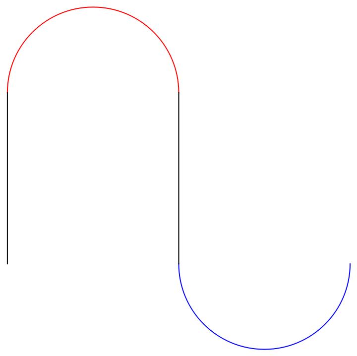
The circular profile we construct with a half circle connected to another half by straight lines as long as , see also the left-hand panel of Figure S1. The average curvature for this profile is then a combination of the constant curvature of the half circles and a zero curvature for the straight parts leading to an average curvature of
| (8) |
For larger circular profiles with we have essentially two circular arcs which are connected to each other (right-hand panel of Figure S1), resulting in
| (9) |
Figure S2 shows the average curvature as a function of the wrinkle wavelength in units of the amplitude. The figure clearly shows that for different values, different profiles are preferred. In the long wavelength limit, the harmonic, i.e., sine-like profile is the lowest curvature solution. The elliptical and circular profile cross at as one would expect since the ellipse reduces to a circle with our definition. For the elliptical profile is preferred and for even smaller wavelength the circular arcs shown in the left panel of Figure S1 become the lowest curvature solution.
However, in several test with different starting geometries for the wrinkles with we found that the relaxed structure does not follow a simple sine wave (or elliptical) profile but that the profiles are composed of a superposition of two sine waves leading to a smoother variation of the curvature in the profiles maxima and minima.
The average and maximum curvature derived from the relaxed positions of the tungsten atoms (cf., main text for details) for all investigated systems are summarized in Tables. 1 and 2.
| Name | Average curvature [1/Å] | Max curvature [1/Å] |
|---|---|---|
| (10,10) | 0.1000 | 0.1481 |
| (11,11) | 0.0057 | 0.1327 |
| (12,12) | 0.0847 | 0.1222 |
| (14,14) | 0.0733 | 0.1042 |
| (15,15) | 0.0721 | 0.1009 |
| (16,16) | 0.0670 | 0.0941 |
| (18,18) | 0.0577 | 0.0803 |
| (24,24) | 0.0439 | 0.0583 |
| (30,30) | 0.0349 | 0.0477 |
| (33,33) | 0.0318 | 0.0442 |
| (41,41) | 0.0256 | 0.0349 |
| (14,0) | 0.1170 | 0.1796 |
| (20,0) | 0.0860 | 0.1246 |
| (24,0) | 0.0728 | 0.1038 |
| (27,0) | 0.0653 | 0.0922 |
| (34,0) | 0.0524 | 0.0733 |
| (39,0) | 0.0459 | 0.0639 |
| (46,0) | 0.0391 | 0.0542 |
| Name | Curvature [1/Å] |
|---|---|
| (10,10) | 0.1044 |
| (11,11) | 0.0955 |
| (12,12) | 0.0883 |
| (13,13) | 0.0818 |
| (14,14) | 0.0764 |
| (15,15) | 0.0715 |
| (16,16) | 0.0672 |
| (18,18) | 0.0600 |
| (24,24) | 0.0453 |
| (30,30) | 0.0364 |
| (33,33) | 0.0332 |
| (41,41) | 0.0267 |
| (56,56) | 0.0196 |
| (14,0) | 0.1236 |
| (20,0) | 0.0905 |
| (24,0) | 0.0765 |
| (27,0) | 0.0685 |
| (34,0) | 0.0550 |
| (39,0) | 0.0481 |
| (46,0) | 0.0410 |
| (58,0) | 0.0326 |
| (65,0) | 0.0291 |
Appendix C Brillouin zone of wrinkles/nanotubes and spin texture
In order to understand the differences in the band structure and the spin texture near the point for wrinkles and nanotubes, we want to briefly summarize, how the Brillouin zone (BZ) for 1D tubes can be derived from a 2D monolayer with hexagonal symmetry.[92]

From a structural perspective, a nanotube of a hexagonal system such as graphene or transition-metal dichalcogenides can be derived from the monolayer which is rolled up to form a tubular structure with a finite radial curvature. The direction of rolling and the circumference of the resultant tube are determined by the chiral vector , where and are the 2D primitive lattice vectors of the corresponding monolayer.[92] The two integer indices and form a pair that specifies the chirality of the tube, with corresponding to armchair tubes, to zigzag tubes, and other cases of being chiral tubes. The translational vector , which is parallel to the tube axis and normal to , reflects the 1D translational symmetry of the nanotube and is defined as:
| (10) | ||||
| (11) |
where denotes the greatest common divisor of the 2 integers and .
In this 1D system, the Bloch wavefunction must be the same after a distance corresponding to the chiral vector , that is, , where is a 2D crystal momentum. This means that the wave vector associated with the circumferential direction becomes quantized. The energy bands of the 1D system thus consist of a set of one-dimensional energy dispersion relations which are cross sections of those of the 2D system as indicated by the colored lines in Figure S4. For more details we refer the interested reader to Ref. 92.
For and large diameter tubes, the main difference between tubes and wrinkles is the boundary condition – while the tubular structure leads to a quantized wave vector which is associated with the circumferential direction , the wrinkle does not have this restriction. The creation of a small amplitude/large wavelength wrinkle is like the formation of a supercell with a perturbation which has the periodicity defined by the wavelength . Thus, the corresponding 1D bandstructure does not consist of “cuts” of the 2D bandstructure but is – for small perturbations – a backfolded version of the full 2D bandstructure in which the “perturbation” due to the curvature leads to a splitting of the bands. Yet, in our structures with the deformation cannot be considered a small perturbation and results in the localization of states in specific regions (cf., Figure 5 in the main text). The band structure is thus a combination of 1D localized systems which are perturbed by the small interactions between them and is very similar to the band structure of the nanotubes with the same curvature as the maximum curvature in the wrinkles.
Interestingly, there are however differences in the spin texture of the valence and conduction bands. Figures S5–S8 show the expectation values of the Pauli matrices for the uppermost 4 valence bands (VB) for an armchair (11,11) nanotube and the corresponding wrinkle of the same size and with wavelength equals four times the radius of the nanotube.

The translational vector in our NTs is parallel to the direction and accordingly the electric field of the induced dipoles is pointing in the / (more specifically it is parallel to , , see also Figure S13). This leads to the following form of the spin-orbit Hamiltonian:
| (12) | ||||
| (13) |
where and with being the azimuth in cylindrical coordinates. One can easily see that the resulting spin texture has only contributions in and and this can also be seen in Figure S5 for the (11,11) wrinkle, however Figure S6 also shows small contributions for . Repeating the calculations with Quantum ESPRESSO[93, 94] (using the structures as obtained with the FHI-aims code, Figures S9–S12) the band structures and the spin textures look the same, except that the x-component of the spin is zero, (as expected) and the do not change the sign when going from one point to the next. We thus attribute this small contribution seen in the FHI-aims calculations to a bug in the plotting routine since both states are degenerate.

There are 2 major differences between nanotubes and wrinkles. While the former always show 2-fold degenerate bands coming from the K and K’ point of the 2D material, the degeneracy is slightly lifted in the wrinkle due to the different strain states along one period of the wrinkle – in fact, a slight asymmetry is also visible in the contour plot of the total electrostatic potential shown in Figure S13. This also leads to a different spin texture in which the VB does not automatically have the opposite spin expectation value of the VB-1.


.

.
.


.


.