Optoelectronic and Transport Properties of Vacancy Ordered Double Perovskite Halides: A First-principles Study
Abstract
In the search for stable lead (Pb) free perovskites, Vacancy ordered double perovskite (VODP), A2BX6 has emerged as a promising class of materials for solar harvesting owing to their nontoxicity, better stability, and unique optoelectronic properties. Recently, this class has been explored for a wide range of applications such as photovoltaics, photodetectors, photocatalysis, and light-emitting diodes. Here, we present the stability and the key physical attributes of few selected compounds in a systematic manner using state-of-the-art first-principle calculations. A careful structural and stability analysis via simulating convex hull and compositional phase diagrams for different structural prototypes discloses 14 stable and 1 metastable compounds in this class. The electronic structure calculations using hybrid functional reveals six compounds to acquire band gap in the ideal visible region. These six compounds, namely Cs2SnI6, Cs2PdI6, Cs2TeI6, Cs2TiI6, Cs2PtI6, and Cs2PdBr6, show high optical absorption ( 105 cm -1) giving rise to high spectroscopic limited maximum efficiency, SLME (15-23%) in the thin-film thickness range. Close inspection of transport properties reveals polar optical phonon scattering to be the dominant mechanism limiting the overall mobility. Further analysis of the polaron excitations discloses the possibility of large polaron formation at low to moderate defect concentrations. At high defect concentrations, ionized impurity scattering takes over. This suggests that, a simulation based guided control of defect concentrations during synthesis can yield a desired candidate for promissing device application. Additionally, few selected compounds show moderate to high electron mobility values (13-63 cm2V-1 s-1) at room temperature. Overall, the present study paves an important path to help design VODP as Pb-free potential candidates for future optoelectronic applications.
I. Introduction
Lead halide perovskites(LHP) have reignited immense research interest in the Photovoltaics (PV) community due to their remarkable power conversion efficiency(PCE) of 25.6% jeong2021pseudo (till date) and affordable device processability. The rapid rise in PCE (3.8% to 25.6%) in a short period of time (2009-2021) is attributed to its high absorption coefficient, high charge carrier mobility, defect tolerance, and cost-effective flexible synthesis. Because of their suitable optoelectronic properties, they have also been explored as photodetectors (PD)li2019enhanced ; huang2021precursor , photocatalysts(PC) zhang2019stable ; yin2021controlling , and light emitting diodes (LED) xu2019rational ; cui2021efficient . Yet, there remains two major challenges in their large scale scalability: (1) Lead (Pb) toxicity and (2) stability in the ambient environment. At present, major research efforts at laboratory scale have been devoted to overcome these issues without losing their original PV performance. lin2020piperidinium ; stolterfoht2018visualization ; giustino2016toward ; shao2018highly ; kangsabanik2020optoelectronic This has led to a detailed exploration of the diverse chemical space of halides perovskites (ABX3)stoumpos2013semiconducting and their derivatives.zhao2017design ; xia2020unveiling ; cai2017computational Among these perovskite derivatives, three major stoichiometric classes have garnered immense research interest. One of the classes namely double perovskites (DP) with stoichiometry A2BB′X6 is mainly generated via transmutation of a combination of trivalent and monovalent elements at B-sites.volonakis2016lead For example, Cs2BiAgBr6,volonakis2016lead ; slavney2016bismuth ; kangsabanik2018double Cs2InAgCl6,volonakis2017cs2inagcl6 etc. belong to DP class which have been extensively explored for various optoelectronic applications. Similarly, A3B2X9 (e.g. Cs3Bi2I9bai2018lead , Cs3Sb2I9singh2018photovoltaic etc.) and A2BX6 (e.g. Cs2SnI6qiu2017unstable , Cs2TiI6ju2018earth etc.) structures are constructed by replacing with trivalent and tetravalent atoms respectively and leaving a vacant B-site. Here, A2BX6 is also called vacancy ordered double perovskite where corner shared alternate BX6 octahedras are removed along all three directions from the unit cell as shown in Figure 1(a).
In the past few years, vacancy-ordered double perovskite family (A2BX6) has gradually drawn ample attention in a wide range of optoelectronic applications owing to their better environmental durability, tunable optical and electronic properties. For example, Cs2SnI6 has been studied as a potential candidate in PVlee2017solution , LED, PDshao2020high ; huang2021precursor , and PC applications due to its direct band gap nature in the visible range( 1.1-1.62 eV), a high absorption coefficient (105 cm-1)qiu2017unstable , a low to high carrier mobility (2-510 cm2 V-1 s-1)lee2014air ; maughan2016defect ; saparov2016thin ; lopez2019optical ; guo2017two . The wide range of measured mobilities of Cs2SnI6 can be attributed to variations resulting from different synthesis and characterization methodologies. Additionally, significant discrepancies have been observed between theoretical and experimental results regarding the transport properties of this material.maughan2018anharmonicity ; maughan2016defect ; cai2017computational ; bhumla2022vacancy The intrinsic limitations to mobility in Cs2SnI6 are still not fully understood, and the underlying scattering mechanisms governing carrier transport remain elusive. Therefore, a comprehensive and systematic study encompassing both theoretical and experimental investigations is highly desired to unravel the mobility ambiguity in Cs2SnI6 and shed light on its transport characteristics. As of now, this compound exhibits a PCE of only 2.1%.lee2017solution In contrast, substitutional alloying in Cs2SnCl6 yields high photoluminescence quantum yield (PLQY) of 95.4% making it promising for further exploration in LED applications.tan2020lead Despite considerable investigation into its structural, electronic, and optical properties, the elucidation of charge-carrier dynamics in Cs2SnI6 still poses challenges that hinder the optimization of conversion efficiencies.
Similarly, Cs2TiBr6, Cs2TeI6, and Cs2PtI6 are also studied experimentally for PV absorbers with their band gaps in the ideal visible range: 1.8, 1.5, and 1.4 eV respectively, along with high absorption coefficients (105 cm-1).vazquez2020vacancy ; schwartz2020air Here, device efficiency for Cs2TiBr6 as PV absorber is reported to be 3.3%.chen2018cesium Indirect band gap and material instability are reported to be responsible for poor PCE in this case. In another report, PV device with Cs2PtI6 shows PCE of 13.88%, which is a remarkable improvement on the reported efficiencies among all the materials belonging to this class till date.schwartz2020air Contribution of larger carrier lifetimes along with direct band gap in ideal visible range and robust stability help Cs2PtI6 to attain the high PCE. There are reports of synthesizing Pdsakai2017solution , and Zrabfalterer2020colloidal based nanomaterials experimentally but not much has been explored in the direction of optoelectronics. These background clearly indicates that A2BX6 class is extremely interesting and fertile from the application perspective, yet a detailed systematic study on their optoelectronic, carrier transport and phonon properties connecting these observations is lacking. Moreover, it is also noticed that substitutional alloying/doping of pure material is an important strategy to improve optoelectronic properties, which again necessitates an in-depth understanding of the pure materials themselves.
In this communication, we present a detailed and systematic study on the A2BX6 class of materials by using highly accurate ab-initio calculations. First, we have performed a thorough stability analysis which includes choice of different structural prototypes, thermodynamical stability via chemical potential phase diagram and convex hull analysis, and lattice dynamics simulation. Next, we have studied the electronic properties of the stable compounds using hybrid (HSE06) functional, which is known to predict reasonably accurate electronic structure information. Optical absroption and PV device parameters are calculated on the promising set of systems showing band gaps in the ideal visible region. Finally, carrier transport properties of these compounds are studied by considering the important scattering mechanisms. The importance of electron-phonon interactions, calculated within the temperature-dependent Feynman polaron model, is also discussed in some detail. We believe that such an in-depth study not only provides a solid physical basis on these class of semiconductors but will also be immensely beneficial for researchers working on their device application in the field of PV, LED, PD, and PC.
II. Structural Properties and Stability
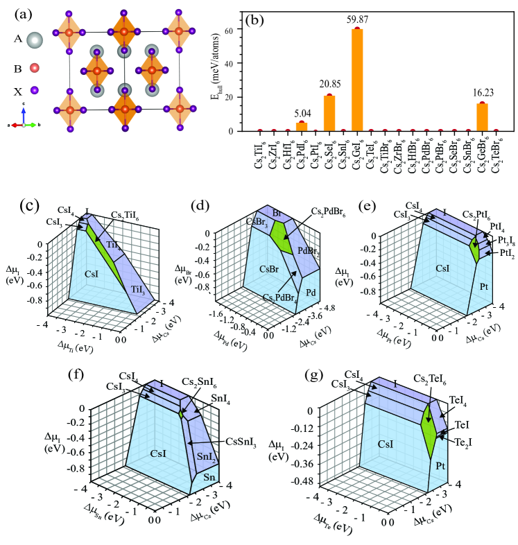
Vacancy ordered double perovskite, A2BX6 is a class of compounds where alternate BX6 octahedra are removed from the ABX3 unit cell as shown in Figure 1(a). In other words, 50% B cations are missing compared to the closed-packed A2BB′X6 perovskite structure. Here, A possesses +1 oxidation state, B has +4 oxidation state and X is halide anion with -1 oxidation state. In general, for perovskites, different crystal structures are possible depending on the ionic radii of the constituent elements. These structures are roughly dictated by few important geometrical factors as defined below,
-
•
Goldschmidt’s tolerance factor:
-
•
Octahedral factor :
-
•
Radius ratio :
In the above expressions, , , and are the empirical ionic radii of the constituent elements A, B, X and the nearest neighbour X-X bond length, respectively in the A2BX6 structure. All the calculated parameters are tabulated in Table S1 of the supplementary information (SI).supplement The calculated Goldschmidt’s tolerance factor predicts formation of cubic structures, which is also consistent with our stability analysis (discussed later) and experimental observations for few of the compounds reported in the literature.ju2018earth ; zhou2018all ; schwartz2020air ; maughan2016defect ; saparov2016thin ; sakai2017solution
In this work, we have investigated the following A2BX6 compounds: A= Cs; B= Ge, Te, Se, Sn, Pd, Pt, Ti, Zr, Hf; X=I, Br. For each compound, we have considered seven most common structural prototypes (as reported in International Crystal Structure Database (ICSD))bergerhoff1983inorganic ; icsd for A2BX6 class of compounds. Space group of these seven structures are Fm-3m (cubic), I4m (tetragonal), I4mmm (tetragonal), P-3m1 (hexagonal), Pnma (orthorhombic), P4mnc (monoclinic), and P121c1 (monoclinic). These crystal structures are shown in Fig. S1 of SI.supplement Most of these structures are very similar in symmetry and differ in energy only within a few meV (3-4 meV). Post structural optimization, the lowest energy structure for most of the above set of compounds turns out to be cubic (Fm-3m). It has been observed experimentally that several Cs based iodide and bromide compounds indeed crystallize in the cubic space group.ju2018earth ; zhou2018all ; schwartz2020air ; maughan2016defect ; saparov2016thin ; sakai2017solution
To further assess the chemical stability, we have calculated the convex hull energies (E) of these compounds with respect to possible secondary phases available in ICSD, open quantum materials database (OQMD)kirklin2015open ; saal2013materials and materials project (MP) databaseWOS:000332272300003 . As evident from Fig. 1(b), most of the compounds lie on the convex hull i.e. E = 0, except Cs2GeI6, Cs2SeI6, Cs2PdI6, and Cs2GeBr6, confirming the stability of the former. For the remaining four compounds E ranges between 5-60 meV/atom, indicating likelihood of chemical (meta/in)stability.
Next, in order to explore the most probable secondary phases during synthesis of Cs2BX6 materials, we have calculated the compositional phase diagrams (chemical potential) for materials on the convex hull. More details about the phase diagram calculations/analysis are given in the Sec. S1(A) of SI.supplement Figure 1(c-g) shows the phase diagrams for those materials which can be potential for optoelectronic applications (based on their band gap, optical and transport properties, as discussed later). The phase diagrams for remaining compounds are displayed in Figure S2 of SI.supplement The green shaded portion shows the stability regions of these materials. The extent of the stability region directly correlates with the ease/difficulty of experimental synthesis.The theoretically optimized lattice parameters and bond lenghts (B-X) of all the stable compounds in their cubic structure are displayed in Table S2 of SI.supplement
Further, we have checked the dynamical stability of these compounds by calculating phonon dispersions as shown in Figure S3 of SI.supplement The absence of any visible imaginary phonon modes indicates dynamical stability of these compounds. For Cs2SnI6 and Cs2TiI6, one can observe small negative phonon frequencies the magnitude of which decreases with increasing supercell size. This is because the later captures the effect of higher order inter-atomic force constants more accurately. This is also evident in previously reported phonon dispersion for Cs2SnI6.bhui2022intrinsically ; jong2019anharmonic Nevertheless, these compounds are already experimentally synthesized, and hence naturally stable.maughan2016defect ; liga2021colloidal
Following stability analysis, we have further studied the electronic structures of 15 (14 stable and 1 metastable) compounds in the next section.
III. Electronic structure
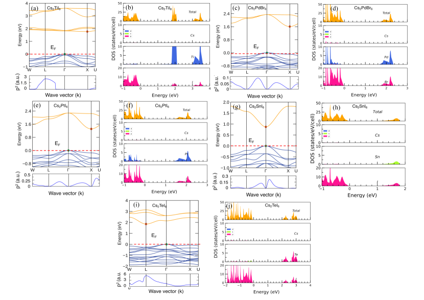
Band structure calculations for all the compounds are initially performed using Perdew-Burke-Ernzerhof (PBE) exchange-correlation functionalperdew1996generalized . As PBE functional is well-known to underestimate the band gap, we also employ hybrid Heyd-Scuseria-Ernzerhof (HSE06)krukau2006influence functional which gives more accurate estimate of band gap in comparison to experiment. Spin-orbit coupling (soc) effect in included in all the calculations. Band structures for four potential compounds calculated using PBE+soc functional (band gaps are scissor shifted to HSE+soc values) are shown in Figure 2. In A2BX6 class of compounds, the topology of band structure calculated using HSE+soc functional is very similar to that calculated using PBE+soc functional except the enlargement of band gap in the former (See Figure S4 of SI for few representative cases).
Figure 2 also shows the optical transition probability, (square of dipole transition matrix elements, p2), and total/orbital projected density of states (PDOS) of Cs2TiI6, Cs2PdBr6, Cs2PtI6, Cs2SnI6, and Cs2TeI6 respectively. The HSE06+soc band gap values for the respective compounds are provided in Table 1. The band structure, PDOS and respective band gap values for other compounds are provided in Figure S5-S7 and Table S3 and S4 of SI.supplement In Fm-3m phase, the estimated band gap values lie within 0.72 eV to 4.31 eV for different compounds. Optical transitions at the fundamental direct gaps are dipole forbidden for all the compounds, as confirmed by the calculated optical transition probability (p2). Here the presence of inversion symmetry plays the key role to induce parity forbidden transitions for these compounds, effectively increasing the optical band gap.
In the present study, we considered 9 different elements at the B site, belonging to 4 distinct groups in the periodic table. Despite all elements having a +4 oxidation state, their valence electron orbital configurations differ, resulting in distinct electronic structures, including variations in band structure and band gap types among the compounds. In the following, we shall discuss the electronic structure of representative compounds from each group and compare them with the electronic structures of other compounds within the same group, including different halides.
For Cs2TiI6, band gap is indirect in nature with conduction band minimum (CBM) at X and valence band maximum (VBM) at . But the direct band gap at is very close to indirect band gap value (50 meV) (Table 1). From the orbital projected density of states (PDOS), we observe that CBM is comprised of Ti-d and I-p i.e. B-d and X-p (see Figure 2)(a,b)). The electronic band gap value is 1.77 eV which is overestimated by 0.75 eV with respect to experimental value (1.02 eV)ju2018earth . The calculated optical band gap lies within 100 meV from the fundamental direct gap. Apart from that, the large difference between the calculated electronic band gap and optically measured experimental band gap can be attributed to the excitonic effect (not taken into account here) and the defects present in the measured sample, as discussed by B.Cucco et.al.cucco2021electronic . All the electronic structure information for the rest of the compounds can be found in Figure S5-S7 and Table S3 and S4 of SI.supplement It is clearly evident that the band gap increases from Ti Zr Hf and also with I Br. In this group, only Cs2TiI6 shows band gap in the ideal visible region.
Cs2PdI6 shows indirect band gap in both the space groups with CBM at X and VBM at (see Fig. S5 of SI). The optically allowed direct band gap (0.88 eV) is very close to the indirect band gap values (0.72 eV) (shown in Table 1 ). Experimentally, Cs2PdI6 nanocrystalszhou2018all are synthesized and and a band gap of 0.69 eV is reported. The reason behind the overestimation might be similar to what is explained for the case of Cs2TiI6. In this case, the CBM is comprised of Pd-d, I-p orbitals while VBM is composed of only I-p orbital (see Fig. S5 of SI). Like Cs2PdI6, Cs2PtI6, Cs2PtBr6, and Cs2PdBr6 show similar orbitals contribution at both CBM and VBM giving rise to indirect nature of band gap. Their band gap values along with the formation energetics and different between direct and indirect band gaps are presented in SI (see Tables S3 and S4 and Fig. S5 and Fig. 2(c,e). For Cs2PtI6 and Cs2PdBr6, the calculated band gap is close to experimentally reported values of Cs2PtI6 powder hamdan2020cs2pti6 ; yang2020novel and Cs2PdBr6 nanocrystals zhou2018all ; sakai2017solution respectively. Here, we observe an increase in band gap going from Pd Pt and also from I Br. In this case, Cs2PdI6, Cs2PtI6, and Cs2PdBr6 compounds show band gaps within the ideal visible range.
The band structure analysis of Cs2TeI6 reveals that it has indirect band gap with a value of 1.85 eV, consistent with the study by Maughan et.al.maughan2016defect . From PDOS analysis, we observe that the CBM is comprised of Te-p and I-p orbitals whereas VBM is made up of I-p orbital (see Figure 2(i) and (j)). The calculated electronic band gap value of 1.85 eV is 0.26 eV higher than the experimentally reported value maughan2016defect . For Cs2TeBr6, the band gap nature and orbital contribution at both CBM and VBM is similar to that of Cs2TeI6. The related electronic properties can be found in SI (see Table. S4 and Fig. S6 ). All the electronic structure information for Cs2SeBr6 can be found in SI (see Table S4 and Figure S6 (c,d) ), which shows similar orbital characteristics.
For Cs2SnI6, the calculated band gap value is 0.85 eV which is direct in nature with band edges (at ) in agreement with the values reported by Maughan et.al.maughan2016defect This is 0.38 eV higher than the experimentally reported value maughan2016defect . From orbital analysis, we observe that the CBM is made up of Sn-s and I-p orbitals, and VBM is comprised of I-p orbital (see Fig. 2(g,h)). For Cs2SnBr6, the band gap nature and orbital contribution at both CBM and VBM remains similar to that of Cs2SnI6. The related electronic properties can be found in SI (see Table S4 and Fig. S6(a,b)).
To summarize the electronic properties, one should note that the calculated electronic band gaps are always overestimated as compared to the experimentally reported optical band gap which is a well-known fact.cucco2021electronic Contrary to previous reports, the optical band gaps are close to the lowest direct band gaps, confirmed by our calculation of optical transition probability. We believe that the most probable reasons for the theoretical overestimation of band gaps can be attributed to the excitonic effects (not included in the present calculations) and defects present in the experimental samples, as discussed by B.Cucco et.al.cucco2021electronic .
From the electronic structure analysis, we notice that the band gaps of Cs2TeI6, Cs2SnI6, Cs2PdI6 (Pnma), Cs2PtI6, Cs2TiI6, and Cs2PdBr6 lie in the ideal visible range for photovoltaic application. Therefore, we shall now focus on the optical properties of these six compounds along with the well-known descriptor ‘Spectroscopic limited maximum efficiency’ (SLME) (as proposed by Yu et.alyu2012identification ) to better understand their potential as solar absorber.
| Compound | (HSE+soc) | JSC | Jmax | VOC | Vmax | FF | SLME | ||
|---|---|---|---|---|---|---|---|---|---|
| (eV) | (eV) | (meV) | (mA cm-2) | (mA cm-2) | (V) | (V) | () | ||
| Cs2TiI6 | 1.02ju2018earth | 1.77 (ID) | 72 | 16.64 | 16.34 | 1.50 | 1.39 | 0.91 | 22.78 |
| Cs2PdBr6 | 1.6sakai2017solution , 1.69 zhou2018all | 1.61 (ID) | 110 | 17.62 | 17.26 | 1.35 | 1.25 | 0.91 | 21.63 |
| Cs2PtI6 | 1.25hamdan2020cs2pti6 , 1.37 yang2020novel , 1.4 schwartz2020air | 1.31 (ID) | 149 | 22.23 | 21.66 | 1.08 | 0.98 | 0.89 | 21.26 |
| Cs2SnI6 | 1.25 maughan2016defect , 1.62 saparov2016thin | 0.87 (D) | 41 | 32.58 | 31.33 | 0.72 | 0.64 | 0.85 | 20.07 |
| Cs2TeI6 | 1.59 maughan2016defect | 1.85 (ID) | 190 | 12.95 | 12.72 | 1.55 | 1.45 | 0.92 | 18.44 |
| Cs2PdI6 | 1.41 zhou2018all | 0.72 (ID) | 166 | 43.20 | 40.94 | 0.54 | 0.46 | 0.81 | 18.97 |
IV. Optical Properties
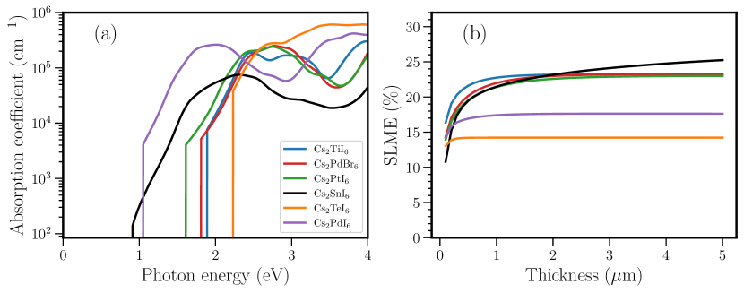
Figure 3(a) shows the absorption coefficients for the above mentioned six promising compounds. All these compounds can act as potential solar absorber as their absorption coefficients are as high as 104-105 cm-1 in the visible range. The optical absorption is contributed by two factors: (1) optical joint density of states (JDOS) and (2) optical transition strength. As we can see in Figure S5(a-d),supplement the square of dipole transition matrix elements (aka transition strength) for Cs2PdI6 is pretty high contributing to better optical absorption. This can be attributed to Cs-p, I-p to Pd-d transition. Apart from that, the JDOS is also likely to be high as the bands near CBM and VBM show flat nature. They are comprised of ‘p’ and ‘d’ orbitals, showing more localized nature as compared to the other compounds. In addition to Cs2PdI6, Cs2SnI6, and Cs2TeI6 also show similar absorption coefficient spectrum. The absorption coefficient is directly related to the frequency dependent dielectric function of a semiconductor via following equation
| (1) |
where is the incident photon energy, is the angular frequency related to via , is the velocity of light, and are the real and imaginary part of the dielectric function respectively. Figure 3(b) shows the thin-film thickness dependance of spectroscopic limited maximum efficiency (SLME), which turn out to be ¿15% for all six compounds. Interestingly, we can see a higher SLME for the Cs2PdI6, Cs2PtI6 and Cs2TiI6 compounds as compared to . Such increased SLME is essentially attributed to increased high absorption spectra due to I-p to Pd/Pt/Ti-d orbital transition as well as suitable band gaps. In Table 1, we present the simulated device parameter values for the six compounds: short-circuit photo-current density (Jsc), open circuit voltage (Voc), fill factor (), maximum current density (Jmax), and maximum voltage (Vmax) obtained from the SLME calculation. The detailed description and method of calculation of these parameters can be found in the SI.supplement As expected, materials with higher band gaps exhibit higher Voc values, while materials with lower band gaps acquire higher Jsc values. The other compounds do not have SLME as high as these six materials owing to higher band gaps. Their absorption coefficients and SLME values are shown in Figure S8 and S9 of SI respectively.supplement Furthermore, it is worth noting that the band gaps of other compounds are distributed within the visible range (larger than 1.8 eV), which makes them suitable for LED and photocatalytic water splitting applications. Alloying at B and x sites are other avenues to tune the optoelectronic properties of these systems and hence make them suitable for different applications.
V. Transport properties
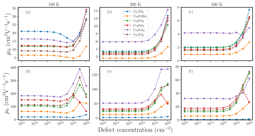
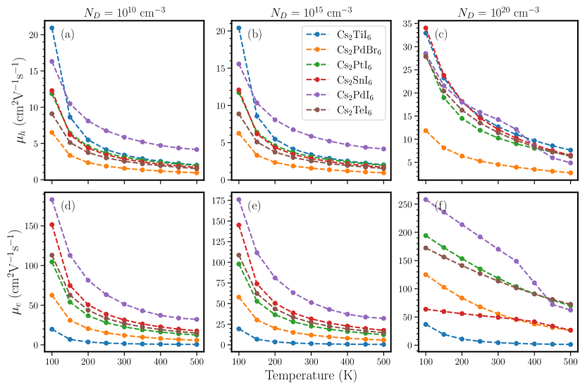
Detailed analysis of optoelectronic properties and calculation of solar efficiency (SLME) reveals six compounds to be promising. This can be attributed to their optimal band gaps falling within the ideal visible region of the solar spectrum coupled with their excellent absorption coefficients. However, in a practical photovoltaic device, extraction of charge carriers is one of the key component determining its power conversion efficiency. As such, mobility of the charge carriers is an integral quantity dictating the promise of a semiconductor for solar harvesting. Most of the past theoretical studies on photovoltaic materials rely on calculation of transport properties based on constant relaxation time approximation (RTA). Within this approximation, all the scattering mechanisms are averaged out via a single relaxation time (chosen to be approximately 10 fs). This practice, however, can be misleading as the carrier relaxation time is a complex parameter which sensitively depends on a number of physical properties and can be significantly different for different materials belonging to the same class (as illustrated in this study). In this section, we perform a thorough analysis of the carrier mobilities of these compounds considering three relevant scattering mechanisms, namely, acoustic phonons (ADP), ionized impurities (IMP), and polar optical phonons (POP) scattering. We have excluded piezoelectric scattering due to the inherent centro-symmetry present in these compounds. In Figure 4 and 5, we show the temperature and defect concentration dependence of electron and hole mobilities ( and ) for these compounds. Contribution of individual scattering mechansims on these mobilities for the six compounds are provided in Figure S10 to S15 of SI.supplement
Figure S16 of SIsupplement displays the total relaxation times of six compounds at varying defect concentrations, ranging from 1010 cm-3 to 1020 cm-3 at three different representative temperatures (100 K, 300 K, and 500 K) for both hole and electron transport. For defect concentrations in the low to moderate range, the relaxation times remains almost constant. However, as the defect concentration increases, relaxation times vary in an irregular manner. To comprehend the cause of this anomalous behavior, a more in-depth analysis was conducted. The relaxation times for all three scattering mechanisms were calculated for each compound, and plotted in Figures S17 to S22.supplement A close inspection of these data confirms that in the low to moderate concentration range, the primary scattering mechanism is due to POP scattering. In contrast, as the concentration increases into the higher range, the dominant scattering mechanism shifts to IMP scattering, resulting in the emergence of anomalous behavior. Such unusual behavior is also reflected in the mobility shown in Fig. 4.
Speaking about the behavior of mobilities for each individual compounds, one can notice that at low temperature (100 K), the hole mobility () is highest for Cs2TiI6 (20.9 cm2V-1 s-1). With increasing temperature, decreases slowly to reach a shallow minimum and increases again with increasing defect concentration. At higher temperature, Cs2PdI6 shows the highest hole mobility (5.9 cm2V-1 s-1 @300 K and 4.2 cm2V-1 s-1 @500 K ) among all the compounds. This compound also shows the highest electron mobility (183 cm2V-1 s-1 @ 100 K, 51 cm2V-1 s-1 @ 300 K, and 32 cm2V-1 s-1 @ 500 K) throughout the temperature range. At room temperature, the hole mobilities remain relatively low but except Cs2TiI6, electron mobilities show moderate to high values (13-63 cm2V-1 s-1). This is commensurate with the electronic band structures of these compounds where the VBM shows flat bands whereas the CBM is more dispersive. Consequently, n-type doping could prove advantageous for efficient charge carrier collection in photovoltaic devices, aligning with the experimental findings for this class of compounds.maughan2018tolerance ; lee2014air ; saparov2016thin A closer look at the individual contributions from the different scattering mechanisms show that at low to moderate defect concentrations ( cm-3), POP scattering is the dominant scattering mechanism limiting the mobilities. With increasing temperatures, the number of activated polar optical phonons increase, and as a result we see a decrease in overall mobility going from 100 K 300 K 500 K. At higher defect concentrations( 1018-1020 cm-3), we see ionized impurity scattering begins to dominate as can be seen from Figures S10(a,b,c)-S15(a,b,c) of SI.supplement At these concentrations, there is one more mechanism that starts to impact the carrier mobility, which is the screening of polar optical phonons by free carriers. This in effect reduces the POP scattering, effectively increasing the overall mobility in some cases. Now, the temperature has also an effect on this screening mechanism. At higher temperatures, there are more activate polar optical phonons, which require a higher density of free carriers to effectively screen the Coulomb field created by these phonons. This is clearly evident from our SI plots (see Figures S10(a,b,c)-S15(a,b,c)).supplement In all the cases, ADP scattering remains low which is common in hybrid perovskites arising out of small deformation potentials.ganose2021efficient ; irvine2021quantifying
In Figure 5(a-f), we show average hole and electron mobilities with respect to temperatures ranging from 100 K to 500 K for three different defect concentrations, low (1010 cm-3), moderate (1015 cm-3) and high (1020 cm-3). Due to weak dependence on IMP scattering in low to moderate defect concentrations, we see the carrier mobility remains similar in these two defect concentrations. But we can see that at higher concentrations, IMP starts to dominate. As such, controlling the defect concentrations can impact device efficiencies, not only because at higher defect concentrations, IMP becomes the dominant scattering mechanism, but also because the prevalence of free carriers will start to screen the POP scattering effect. As expected, the overall mobility has a strong temperature dependence for most of the compounds and remains high to moderate for the electrons whereas the hole mobility values remain consistently low.
The above analysis reveals that in A2BX6 class, polar optical phonons play a dominant role at the realistic defect concentrations relevant for photovoltaic application. As such, next we study the properties of the polaronic states via calculating the Frhlich interactions under the temperature-dependent Feynman polaron model.feynman1955slow [Reference] In polar semiconductors, for example, halide perovskite and its derivatives, the interaction between charge carriers and the macroscopic electric field generated by longitudinal optical phonon (LO) is well known to be the dominant scattering mechanism near room temperature which is expected to be the case for our studied materials as well.hellwarth1999mobility ; manna2020lattice ; maughan2018anharmonicity ; maughan2018tolerance ; ganose2021efficient To investigate the same, we studied the influence of changing B-site in A2BX6 on the electron-phonon coupling (EPC). Within the Frhlich interaction model, the interaction strength () is defined as
| (2) |
were, is dielectric constant of vacuum, and are high frequency and static dielectric constants of the semiconductor, is the reduced Plank constant, is the characteristic angular LO frequency where all the infrared active optical phonon branches are taken into account via a spectral average,hellwarth1999mobility is the carrier effective mass. Table 2 display all the associated values related to Frhlich interaction for electrons for the six compounds. The corresponding list of parameters for the holes for these six compounds are reported in Table S5 of SM.supplement To validate our simulation, we compare the calculated values of for Cs2SnI6, with recent literature and observe a fair agreement.maughan2018anharmonicity In case of A2BX6 class, calculated -values lie in the moderate range (1 6). Estimated values of polaron radius (lp) indicates formation of large polarons, similar to what is observed for hybrid halide perovskites and double perovskites.hellwarth1999mobility ; manna2020lattice ; saxena2020contrasting value is highest for Cs2TiI6 mainly due to higher electron effective mass compared to the other compounds. Additionally, taking an inference from the electronic structure of these materials, we see that CBM in Cs2TiI6 has a contribution from Ti-d and I-p orbitals whereas for Cs2SnI6, it is Sn-s and I-p orbitals. Now, Ti-d orbitals are more localized arising out of the flat band and hence higher effective mass. For other compounds, we see more dispersive bands (see Figure 2) at CBM, and the corresponding values are in the range close to that of Cs2SnI6. Interestingly, the hole mobility turn out to be significantly lower than the electron mobility. To conclude, large polaron is the main carrier related to moderate mobility for our studied compounds. These crucial observations clearly indicates the importance of studying charge carrier behavior in A2BX6 class of compounds and its implications in future applications.
| Parameters | Cs2TiI6 | Cs2PdBr6 | Cs2PtI6 | Cs2SnI6 | Cs2TeI6 | Cs2PdI6 |
|---|---|---|---|---|---|---|
| me∗(m0) | 1.66 | 0.66 | 0.49 | 0.31 | 0.35 | 0.61 |
| 4.91 | 4.15 | 4.82 | 5.04 | 4.89 | 7.58 | |
| 10.81 | 7.21 | 8.40 | 10.41 | 11.21 | 11.68 | |
| (THz) | 3.77 | 3.16 | 2.16 | 2.60 | 2.71 | 2.25 |
| 4.23 | 2.66 | 2.44 | 2.02 | 2.38 | 1.38 | |
| (cm2V-1 s-1) | 1.5 | 11.9 | 22.7 | 31.4 | 27 | 51.3 |
| l(Å) | 29.40 | 32.75 | 25.88 | 32.48 | 30.92 | 35.33 |
VI. Conclusion
In summary, we performed an accurate and systematic investigation of Pb-free vacancy ordered double perovskites (A2BX6) from the optoelectronic application perspective. We carried out a thorough stability analysis considering different structural prototypes and carefully simulating the convex hull energy diagram including all possible secondary phases. We found 14 compounds to be stable and 1 in the metastable phase. For stable compounds, we further simulated the compositional phase diagrams to assist the experimentalists identifying the most probable secondary phases which might emerge during synthesis. Next, a carefull electronic structure analysis reveals six compounds, namely Cs2TeI6, Cs2SnI6, Cs2PdI6, Cs2PtI6, Cs2TiI6, and Cs2PdBr6 to possess optically allowed band gaps in the ideal visible range (0.8-1.85 eV). The detailed investigation of optical properties confirms that few of these compounds possess favorable optoelectronic properties facilitating better efficiency than some of the existing ones. A close inspection of transport properties reveals that Cs2PdBr6, Cs2PtI6, Cs2SnI6, Cs2PdI6, and Cs2TeI6 compounds acquire moderate to high electron mobilities (13 - 63 cm2V-1 s-1). In all the cases, polar optical phonons (POP) remain the dominant scattering mechanism at low to moderate defect concentrations. At high defect concentrations, ionized impurity scattering starts to dominate while accumulation of free carriers shows a screening effect on the POP scattering. This study is expected to facilitate the necessary base and guidance for future experimental synthesis of some of these compounds to achieve desired features for promising device applications.
VII. Computational Details
First-principles calculations are carried out using density functional theory (DFT)PhysRev.140.A1133 with projector augmented wave (PAW)blochl1994projector basis set as implemented in Vienna Ab-Initio Simulation Package (VASP).PhysRevB.59.1758 ; kresse1993ab ; kresse1994ab ; kresse1996efficient ; KRESSE199615 A plane wave energy cutoff of 520 eV, -centered 4 44 k-mesh, and Perdew-Burke-Ernzerhof (PBE) exchange-correlation functionalperdew1996generalized were employed to perform the geometry optimization. The crystal structure was relaxed with force tolerance criteria of 0.001 eVÅ-1. The spin-orbit coupling (soc) effect is included while simulating the electronic and optical properties. Hybrid(HSE06) functionalkrukau2006influence is used to calculate the band gap and band edges which are known to provide a more accurate estimate for the same. Optical absorption spectra are simulated within the independent particle approximation and then the absorption onset value is scissor shifted to HSE06 band gap values. This method makes it possible to accurately assess the SLME for the materials under consideration. The chemical phase diagrams are drawn using Chesta software package.chesta Phonon dispersion is calculated using the density functional perturbation theory (DFPT) using -centered 444 k-mesh under the supercell method. The 2nd order force constant is calculated using 222 supercells of primitive cells for cubic structures and in similar proportion for other structures. Next, the rotational sum rule is applied using the hiphive packageeriksson2019hiphive to renormalize the phonon frequencies. Transport calculations are performed using the AMSET code,ganose2021efficient , where we have considered three different scattering mechanisms, namely scattering due to acoustic phonons (ADP), ionized impurities (IMP), and polar optical phonons (POP). Piezoelectric scattering is not included due to the centro-symmetric crystal structure of A2BX6, whereas screening due to free carriers at high defect concentrations is included. This program uses the Boltzmann transport equation’s (BTE) momentum relaxation time approximation (MRTA) to determine scattering rates and carrier mobilities. Polaron related parameters were simulated via implementing a temperature dependent Feynman polaron model.hellwarth1999mobility ; frost2017calculating Born effective charges and static and high-frequency dielectric tensors were calculated using density functional perturbation theory (DFPT) as implemented in VASP. The effective mass has been calculated using the following equation:
| (3) |
where, is the effective mass in the -th direction (=x,y,z).mortensen2005real ; enkovaara2010electronic ; larsen2017atomic ; kangsabanik2022indirect
VIII. Acknowledgments
SG acknowledges financial support from IIT Bombay for research fellowship. AA and MA acknowledges National Center for Photovoltaic Research and Education (NCPRE) funded by Ministry of new renewable energy (MNRE), Government of India, and IIT Bombay for possible funding to support this research.
References
- [1] Jaeki Jeong, Minjin Kim, Jongdeuk Seo, Haizhou Lu, Paramvir Ahlawat, Aditya Mishra, Yingguo Yang, Michael A Hope, Felix T Eickemeyer, Maengsuk Kim, et al. Pseudo-halide anion engineering for -FAPbI3 perovskite solar cells. Nature, 592(7854):381–385, 2021.
- [2] Leqi Li, Xin Liu, Hongjian Zhang, Binbin Zhang, Wanqi Jie, Paul J Sellin, Chuanhao Hu, Guoqiang Zeng, and Yadong Xu. Enhanced X-ray sensitivity of MAPbBr3 detector by tailoring the interface-states density. ACS applied materials & interfaces, 11(7):7522–7528, 2019.
- [3] Junyi Huang, Chen Dong, Yantao Mei, Xiayao Lu, Gentian Yue, Yueyue Gao, Rong Liu, Weifeng Zhang, and Furui Tan. The precursor-compensation strategy boosts the photoresponse performance of air-stable, self-powered Cs2SnI6 photodetectors. Journal of Materials Chemistry C, 9(40):14217–14225, 2021.
- [4] Zhenzhen Zhang, Yongqi Liang, Hanlin Huang, Xingyi Liu, Qi Li, Langxing Chen, and Dongsheng Xu. Stable and highly efficient photocatalysis with lead-free double-perovskite of Cs2AgBiBr6. Angewandte Chemie International Edition, 58(22):7263–7267, 2019.
- [5] Hang Yin, Junsheng Chen, Peng Guan, Daoyuan Zheng, Qingkun Kong, Songqiu Yang, Panwang Zhou, Bin Yang, Tönu Pullerits, and Keli Han. Controlling Photoluminescence and Photocatalysis Activities in Lead-Free Cs2PtxSn1-xCl6 Perovskites via Ion Substitution. Angewandte Chemie, 133(42):22875–22881, 2021.
- [6] Weidong Xu, Qi Hu, Sai Bai, Chunxiong Bao, Yanfeng Miao, Zhongcheng Yuan, Tetiana Borzda, Alex J Barker, Elizaveta Tyukalova, Zhangjun Hu, et al. Rational molecular passivation for high-performance perovskite light-emitting diodes. Nature Photonics, 13(6):418–424, 2019.
- [7] Jieyuan Cui, Yang Liu, Yunzhou Deng, Chen Lin, Zhishan Fang, Chensheng Xiang, Peng Bai, Kai Du, Xiaobing Zuo, Kaichuan Wen, et al. Efficient light-emitting diodes based on oriented perovskite nanoplatelets. Science advances, 7(41):eabg8458, 2021.
- [8] Yen-Hung Lin, Nobuya Sakai, Peimei Da, Jiaying Wu, Harry C Sansom, Alexandra J Ramadan, Suhas Mahesh, Junliang Liu, Robert DJ Oliver, Jongchul Lim, et al. A piperidinium salt stabilizes efficient metal-halide perovskite solar cells. Science, 369(6499):96–102, 2020.
- [9] Martin Stolterfoht, Christian M Wolff, José A Márquez, Shanshan Zhang, Charles J Hages, Daniel Rothhardt, Steve Albrecht, Paul L Burn, Paul Meredith, Thomas Unold, et al. Visualization and suppression of interfacial recombination for high-efficiency large-area pin perovskite solar cells. Nature Energy, 3(10):847–854, 2018.
- [10] Feliciano Giustino and Henry J Snaith. Toward lead-free perovskite solar cells. ACS Energy Letters, 1(6):1233–1240, 2016.
- [11] Shuyan Shao, Jian Liu, Giuseppe Portale, Hong-Hua Fang, Graeme R Blake, Gert H ten Brink, L Jan Anton Koster, and Maria Antonietta Loi. Highly reproducible Sn-based hybrid perovskite solar cells with 9% efficiency. Advanced Energy Materials, 8(4):1702019, 2018.
- [12] Jiban Kangsabanik, Supriti Ghorui, M Aslam, and Aftab Alam. Optoelectronic Properties and Defect Physics of Lead-Free Photovoltaic Absorbers Cs2AuIAuIIIX6 (X= I, Br). Physical Review Applied, 13(1):014005, 2020.
- [13] Constantinos C Stoumpos, Christos D Malliakas, and Mercouri G Kanatzidis. Semiconducting tin and lead iodide perovskites with organic cations: phase transitions, high mobilities, and near-infrared photoluminescent properties. Inorganic chemistry, 52(15):9019–9038, 2013.
- [14] Xin-Gang Zhao, Ji-Hui Yang, Yuhao Fu, Dongwen Yang, Qiaoling Xu, Liping Yu, Su-Huai Wei, and Lijun Zhang. Design of lead-free inorganic halide perovskites for solar cells via cation-transmutation. Journal of the American Chemical Society, 139(7):2630–2638, 2017.
- [15] Mengling Xia, Jun-Hui Yuan, Guangda Niu, Xinyuan Du, Lixiao Yin, Weicheng Pan, Jiajun Luo, Zhigang Li, Hongtao Zhao, Kan-Hao Xue, et al. Unveiling the structural descriptor of A3B2X9 perovskite derivatives toward X-ray detectors with low detection limit and high stability. Advanced Functional Materials, 30(24):1910648, 2020.
- [16] Yao Cai, Wei Xie, Hong Ding, Yan Chen, Krishnamoorthy Thirumal, Lydia H Wong, Nripan Mathews, Subodh G Mhaisalkar, Matthew Sherburne, and Mark Asta. Computational study of halide perovskite-derived A2BX6 inorganic compounds: chemical trends in electronic structure and structural stability. Chemistry of Materials, 29(18):7740–7749, 2017.
- [17] George Volonakis, Marina R Filip, Amir Abbas Haghighirad, Nobuya Sakai, Bernard Wenger, Henry J Snaith, and Feliciano Giustino. Lead-free halide double perovskites via heterovalent substitution of noble metals. The journal of physical chemistry letters, 7(7):1254–1259, 2016.
- [18] Adam H Slavney, Te Hu, Aaron M Lindenberg, and Hemamala I Karunadasa. A bismuth-halide double perovskite with long carrier recombination lifetime for photovoltaic applications. Journal of the American chemical society, 138(7):2138–2141, 2016.
- [19] Jiban Kangsabanik, Vipinraj Sugathan, Anuradha Yadav, Aswani Yella, and Aftab Alam. Double perovskites overtaking the single perovskites: A set of new solar harvesting materials with much higher stability and efficiency. Physical Review Materials, 2(5):055401, 2018.
- [20] George Volonakis, Amir Abbas Haghighirad, Rebecca L Milot, Weng H Sio, Marina R Filip, Bernard Wenger, Michael B Johnston, Laura M Herz, Henry J Snaith, and Feliciano Giustino. Cs2InAgCl6: a new lead-free halide double perovskite with direct band gap. The journal of physical chemistry letters, 8(4):772–778, 2017.
- [21] Fan Bai, Yonghong Hu, Yanqiang Hu, Ting Qiu, Xiaoliang Miao, and Shufang Zhang. Lead-free, air-stable ultrathin Cs3Bi2I9 perovskite nanosheets for solar cells. Solar energy materials and solar cells, 184:15–21, 2018.
- [22] Anupriya Singh, Karunakara Moorthy Boopathi, Anisha Mohapatra, Yang Fang Chen, Gang Li, and Chih Wei Chu. Photovoltaic performance of vapor-assisted solution-processed layer polymorph of Cs3Sb2I9. ACS applied materials & interfaces, 10(3):2566–2573, 2018.
- [23] Xiaofeng Qiu, Bingqiang Cao, Shuai Yuan, Xiangfeng Chen, Zhiwen Qiu, Yanan Jiang, Qian Ye, Hongqiang Wang, Haibo Zeng, Jian Liu, et al. From unstable CsSnI3 to air-stable Cs2SnI6: A lead-free perovskite solar cell light absorber with bandgap of 1.48 eV and high absorption coefficient. Solar Energy Materials and Solar Cells, 159:227–234, 2017.
- [24] Ming-Gang Ju, Min Chen, Yuanyuan Zhou, Hector F Garces, Jun Dai, Liang Ma, Nitin P Padture, and Xiao Cheng Zeng. Earth-abundant nontoxic titanium (IV)-based vacancy-ordered double perovskite halides with tunable 1.0 to 1.8 eV bandgaps for photovoltaic applications. ACS Energy Letters, 3(2):297–304, 2018.
- [25] Byunghong Lee, Anthony Krenselewski, Sung Il Baik, David N Seidman, and Robert PH Chang. Solution processing of air-stable molecular semiconducting iodosalts, Cs2SnI6-xBrx, for potential solar cell applications. Sustainable Energy & Fuels, 1(4):710–724, 2017.
- [26] Dali Shao, Weiguang Zhu, Guoqing Xin, Xueqing Liu, Tianmeng Wang, Sufei Shi, Jie Lian, and Shayla Sawyer. A high performance UV–visible dual-band photodetector based on an inorganic Cs2SnI6 perovskite/ZnO heterojunction structure. Journal of Materials Chemistry C, 8(5):1819–1825, 2020.
- [27] Byunghong Lee, Constantinos C Stoumpos, Nanjia Zhou, Feng Hao, Christos Malliakas, Chen-Yu Yeh, Tobin J Marks, Mercouri G Kanatzidis, and Robert PH Chang. Air-stable molecular semiconducting iodosalts for solar cell applications: Cs2SnI6 as a hole conductor. Journal of the American Chemical Society, 136(43):15379–15385, 2014.
- [28] Annalise E Maughan, Alex M Ganose, Mitchell M Bordelon, Elisa M Miller, David O Scanlon, and James R Neilson. Defect tolerance to intolerance in the vacancy-ordered double perovskite semiconductors Cs2SnI6 and Cs2TeI6. Journal of the American Chemical Society, 138(27):8453–8464, 2016.
- [29] Bayrammurad Saparov, Jon-Paul Sun, Weiwei Meng, Zewen Xiao, Hsin-Sheng Duan, Oki Gunawan, Donghyeop Shin, Ian G Hill, Yanfa Yan, and David B Mitzi. Thin-film deposition and characterization of a Sn-deficient perovskite derivative Cs2SnI6. Chemistry of Materials, 28(7):2315–2322, 2016.
- [30] Eduardo López-Fraguas, Sofia Masi, and Ivan Mora-Sero. Optical characterization of lead-free Cs2SnI6 double perovskite fabricated from degraded and reconstructed CsSnI3 films. ACS Applied Energy Materials, 2(12):8381–8387, 2019.
- [31] Fawen Guo, Zonghuan Lu, Dibyajyoti Mohanty, Tianmeng Wang, Ishwara B Bhat, Shengbai Zhang, Sufei Shi, Morris A Washington, Gwo-Ching Wang, and Toh-Ming Lu. A two-step dry process for Cs2SnI6 perovskite thin film. Materials Research Letters, 5(8):540–546, 2017.
- [32] Annalise E Maughan, Alex M Ganose, Andrew M Candia, Juliette T Granger, David O Scanlon, and James R Neilson. Anharmonicity and octahedral tilting in hybrid vacancy-ordered double perovskites. Chemistry of Materials, 30(2):472–483, 2018.
- [33] Preeti Bhumla, Manjari Jain, Sajjan Sheoran, and Saswata Bhattacharya. Vacancy-ordered double perovskites cs2bi6 (b= pt, pd, te, sn): An emerging class of thermoelectric materials. The Journal of Physical Chemistry Letters, 13:11655–11662, 2022.
- [34] Zhifang Tan, Yanmeng Chu, Jinxi Chen, Jinghui Li, Guoqi Ji, Guangda Niu, Liang Gao, Zewen Xiao, and Jiang Tang. Lead-free perovskite variant solid solutions Cs2Sn1-xTexCl6: bright luminescence and high anti-water stability. Advanced Materials, 32(32):2002443, 2020.
- [35] Isabel Vazquez-Fernandez, Silvia Mariotti, Oliver S Hutter, Max Birkett, Tim D Veal, Theodore DC Hobson, Laurie J Phillips, Lefteris Danos, Pabitra K Nayak, Henry J Snaith, et al. Vacancy-ordered double perovskite Cs2TeI6 thin films for optoelectronics. Chemistry of Materials, 32(15):6676–6684, 2020.
- [36] Dakota Schwartz, Rubaiya Murshed, Harry Larson, Benedikt Usprung, Sina Soltanmohamad, Ramesh Pandey, Edward S Barnard, Angus Rockett, Thomas Hartmann, Ivano E Castelli, et al. Air Stable, High-Efficiency, Pt-Based Halide Perovskite Solar Cells with Long Carrier Lifetimes. physica status solidi (RRL)–Rapid Research Letters, 14(8):2000182, 2020.
- [37] Min Chen, Ming-Gang Ju, Alexander D Carl, Yingxia Zong, Ronald L Grimm, Jiajun Gu, Xiao Cheng Zeng, Yuanyuan Zhou, and Nitin P Padture. Cesium titanium (IV) bromide thin films based stable lead-free perovskite solar cells. Joule, 2(3):558–570, 2018.
- [38] Nobuya Sakai, Amir Abbas Haghighirad, Marina R Filip, Pabitra K Nayak, Simantini Nayak, Alexandra Ramadan, Zhiping Wang, Feliciano Giustino, and Henry J Snaith. Solution-processed cesium hexabromopalladate (IV), Cs2PdBr6, for optoelectronic applications. Journal of the American Chemical Society, 139(17):6030–6033, 2017.
- [39] Anna Abfalterer, Javad Shamsi, Dominik J Kubicki, Christopher N Savory, James Xiao, Giorgio Divitini, Weiwei Li, Stuart Macpherson, Krzysztof Gałkowski, Judith L MacManus-Driscoll, et al. Colloidal synthesis and optical properties of perovskite-inspired cesium zirconium halide nanocrystals. ACS materials letters, 2(12):1644–1652, 2020.
- [40] See the Supplementary material. It contains details about different further structural properties, stability, further electronic structure data, transition probability, further optical data, and transport related properties. It also contains brief discussion about SLME can be found which includes ref [55, 77, 78, 79].
- [41] Lei Zhou, Jin-Feng Liao, Zeng-Guang Huang, Xu-Dong Wang, Yang-Fan Xu, Hong-Yan Chen, Dai-Bin Kuang, and Cheng-Yong Su. All-inorganic lead-free Cs2PdX6 (X= Br, I) perovskite nanocrystals with single unit cell thickness and high stability. ACS Energy Letters, 3(10):2613–2619, 2018.
- [42] Guenter Bergerhoff, R Hundt, R Sievers, and ID Brown. The inorganic crystal structure data base. Journal of chemical information and computer sciences, 23(2):66–69, 1983.
- [43] Inorganic Crystal Structure Database (ICSD) https://icsd.fiz-karlsruhe.de.
- [44] Scott Kirklin, James E Saal, Bryce Meredig, Alex Thompson, Jeff W Doak, Muratahan Aykol, Stephan Rühl, and Chris Wolverton. The open quantum materials database (oqmd): assessing the accuracy of dft formation energies. npj Computational Materials, 1(1):1–15, 2015.
- [45] James E Saal, Scott Kirklin, Muratahan Aykol, Bryce Meredig, and Christopher Wolverton. Materials design and discovery with high-throughput density functional theory: the open quantum materials database (oqmd). Jom, 65:1501–1509, 2013.
- [46] Anubhav Jain, Shyue Ping Ong, Geoffroy Hautier, Wei Chen, William Davidson Richards, Stephen Dacek, Shreyas Cholia, Dan Gunter, David Skinner, Gerbrand Ceder, and Kristin A. Persson. Commentary: The materials project: A materials genome approach to accelerating materials innovation. APL MATERIALS, 1(1), JUL 2013.
- [47] Animesh Bhui, Tanmoy Ghosh, Koushik Pal, Kewal Singh Rana, Kaushik Kundu, Ajay Soni, and Kanishka Biswas. Intrinsically low thermal conductivity in the n-type vacancy-ordered double perovskite Cs2SnI6: octahedral rotation and anharmonic rattling. Chemistry of Materials, 34(7):3301–3310, 2022.
- [48] Un-Gi Jong, Chol-Jun Yu, Yun-Hyok Kye, Song-Hyok Choe, Jin-Song Kim, and Yong-Guk Choe. Anharmonic phonons and phase transitions in the vacancy-ordered double perovskite cs 2 sni 6 from first-principles predictions. Physical Review B, 99(18):184105, 2019.
- [49] Shanti Maria Liga and Gerasimos Konstantatos. Colloidal synthesis of lead-free Cs2TiBr6-xIx perovskite nanocrystals. Journal of Materials Chemistry C, 9(34):11098–11103, 2021.
- [50] John P Perdew, Kieron Burke, and Matthias Ernzerhof. Generalized gradient approximation made simple. Physical review letters, 77(18):3865, 1996.
- [51] Aliaksandr V Krukau, Oleg A Vydrov, Artur F Izmaylov, and Gustavo E Scuseria. Influence of the exchange screening parameter on the performance of screened hybrid functionals. The Journal of chemical physics, 125(22):224106, 2006.
- [52] Bruno Cucco, Gaëlle Bouder, Laurent Pedesseau, Claudine Katan, Jacky Even, Mikael Kepenekian, and George Volonakis. Electronic structure and stability of Cs2TiX6 and Cs2ZrX6 (X= Br, I) vacancy ordered double perovskites. Applied Physics Letters, 119(18):181903, 2021.
- [53] Muhammed Hamdan and Aravind Kumar Chandiran. Cs2PtI6 halide perovskite is stable to air, moisture, and extreme pH: application to photoelectrochemical solar water oxidation. Angewandte Chemie, 132(37):16167–16172, 2020.
- [54] Shuzhang Yang, Liang Wang, Shuai Zhao, Anmin Liu, Yi Zhou, Qianji Han, Fengyang Yu, Liguo Gao, Chu Zhang, and Tingli Ma. Novel lead-free material Cs2PtI6 with narrow bandgap and ultra-stability for its photovoltaic application. ACS Applied Materials & Interfaces, 12(40):44700–44709, 2020.
- [55] Liping Yu and Alex Zunger. Identification of potential photovoltaic absorbers based on first-principles spectroscopic screening of materials. Physical review letters, 108(6):068701, 2012.
- [56] Annalise E Maughan, Alex M Ganose, Mohammed A Almaker, David O Scanlon, and James R Neilson. Tolerance factor and cooperative tilting effects in vacancy-ordered double perovskite halides. Chemistry of Materials, 30(11):3909–3919, 2018.
- [57] Alex M Ganose, Junsoo Park, Alireza Faghaninia, Rachel Woods-Robinson, Kristin A Persson, and Anubhav Jain. Efficient calculation of carrier scattering rates from first principles. Nature communications, 12(1):2222, 2021.
- [58] Lewis AD Irvine, Alison B Walker, and Matthew J Wolf. Quantifying polaronic effects on the scattering and mobility of charge carriers in lead halide perovskites. Physical Review B, 103(22):L220305, 2021.
- [59] Richard Phillips Feynman. Slow electrons in a polar crystal. Physical Review, 97(3):660, 1955.
- [60] Robert W Hellwarth and Ivan Biaggio. Mobility of an electron in a multimode polar lattice. Physical Review B, 60(1):299, 1999.
- [61] Debjit Manna, Jiban Kangsabanik, Tapan Kumar Das, Debashish Das, Aftab Alam, and Aswani Yella. Lattice Dynamics and Electron–Phonon Coupling in Lead-Free Cs2AgIn1-xBixCl6 Double Perovskite Nanocrystals. The Journal of Physical Chemistry Letters, 11(6):2113–2120, 2020.
- [62] Rishabh Saxena, Jiban Kangsabanik, Ayush Kumar, Aga Shahee, Shivam Singh, Nakul Jain, Supriti Ghorui, Vinod Kumar, Avinash V Mahajan, Aftab Alam, et al. Contrasting temperature dependence of the band gap in CH3NH3PbX3 (X= I, Br, Cl): Insight from lattice dilation and electron-phonon coupling. Physical Review B, 102(8):081201, 2020.
- [63] W. Kohn and L. J. Sham. Self-Consistent Equations Including Exchange and Correlation Effects. Phys. Rev., 140:A1133–A1138, Nov 1965.
- [64] Peter E Blöchl. Projector augmented-wave method. Physical review B, 50(24):17953, 1994.
- [65] G. Kresse and D. Joubert. From ultrasoft pseudopotentials to the projector augmented-wave method. Phys. Rev. B, 59:1758–1775, Jan 1999.
- [66] Georg Kresse and Jürgen Hafner. Ab initio molecular dynamics for liquid metals. Physical review B, 47(1):558, 1993.
- [67] Georg Kresse and Jürgen Hafner. Ab initio molecular-dynamics simulation of the liquid-metal–amorphous-semiconductor transition in germanium. Physical Review B, 49(20):14251, 1994.
- [68] Georg Kresse and Jürgen Furthmüller. Efficient iterative schemes for ab initio total-energy calculations using a plane-wave basis set. Physical review B, 54(16):11169, 1996.
- [69] G. Kresse and J. Furthmüller. Efficiency of ab-initio total energy calculations for metals and semiconductors using a plane-wave basis set. Computational Materials Science, 6(1):15–50, 1996.
- [70] N. CHESTA Hatada. Available at http://www.aqua.mtl.kyoto-u.ac.jp/chestaEng.html (2010).
- [71] Fredrik Eriksson, Erik Fransson, and Paul Erhart. The hiphive package for the extraction of high-order force constants by machine learning. Advanced Theory and Simulations, 2(5):1800184, 2019.
- [72] Jarvist Moore Frost. Calculating polaron mobility in halide perovskites. Physical Review B, 96(19):195202, 2017.
- [73] Jens Jørgen Mortensen, Lars Bruno Hansen, and Karsten Wedel Jacobsen. Real-space grid implementation of the projector augmented wave method. Physical review B, 71(3):035109, 2005.
- [74] Jussi Enkovaara, Carsten Rostgaard, J Jørgen Mortensen, Jingzhe Chen, M Dułak, Lara Ferrighi, Jeppe Gavnholt, Christian Glinsvad, V Haikola, HA Hansen, et al. Electronic structure calculations with gpaw: a real-space implementation of the projector augmented-wave method. Journal of physics: Condensed matter, 22(25):253202, 2010.
- [75] Ask Hjorth Larsen, Jens Jørgen Mortensen, Jakob Blomqvist, Ivano E Castelli, Rune Christensen, Marcin Dułak, Jesper Friis, Michael N Groves, Bjørk Hammer, Cory Hargus, et al. The atomic simulation environment—a python library for working with atoms. Journal of Physics: Condensed Matter, 29(27):273002, 2017.
- [76] Jiban Kangsabanik, Mark Kamper Svendsen, Alireza Taghizadeh, Andrea Crovetto, and Kristian S Thygesen. Indirect band gap semiconductors for thin-film photovoltaics: High-throughput calculation of phonon-assisted absorption. Journal of the American Chemical Society, 144(43):19872–19883, 2022.
- [77] William Shockley and Hans J Queisser. Detailed balance limit of efficiency of p-n junction solar cells. Journal of applied physics, 32(3):510-519, 1961.
- [78] M. A. Green. Third generation photovoltaics: advanced solar energy conversion Physics Today, 57(12):71-72, 2004.
- [79] Tom Tiedje, ELI Yablonovitch, George D Cody, and Bonnie G Brooks. Limiting efficiency of silicon solar cells. IEEE Transactions on electron devices, 31(5):711-716, 1984.