Design and Validation of a Metallic Reflectarray for Communications at True Terahertz Frequencies
Abstract.
Wireless communications in the terahertz band () is a promising and key wireless technology enabling ultra-high data rate communication over multi-gigahertz-wide bandwidths, thus fulfilling the demand for denser networks. The complex propagation environment at such high frequencies introduces several challenges, such as high spreading and molecular absorption losses. As such, intelligent reflecting surfaces have been proposed as a promising solution to enable communication in the presence of blockage or to aid a resource-limited quasi-omnidirectional transmitter direct its radiated power. In this paper, we present a metallic reflectarray design achieving controlled non-specular reflection at true terahertz frequencies (i.e., ). We conduct extensive experiments to further characterize and validate its working principle using terahertz time-domain spectroscopy and demonstrate its effectiveness with information-carrying signals using a continuous-wave terahertz testbed. Our results show that the reflectarray can help facilitate robust communication links over non-specular paths and improve the reliability of terahertz communications, thereby unleashing the true potential of the terahertz band.
1. Introduction
The terahertz (THz) band has been envisioned as a key asset for the next generation of wireless communication and sensing systems (Akyildiz et al., 2022). The very large bandwidth available at THz frequencies (easily tens to hundreds of gigahertz) opens the door to terabit-per-second links in front-haul applications, as in wireless immersive extended reality (XR), and up to hundred gigabits per second (Gbps) in wireless backhaul applications, which can bridge the rural digital divide. In addition, the shorter wavelength of THz signals opens the door to sub-millimetric resolution in radar applications. Moreover, the shorter wavelength also leads to smaller antennas that can be leveraged in nanonetworking applications (Jornet and Sangwan, 2023), including wireless networks-on-chip or wireless nano-bio sensor and actuator networks. Finally, the low but non-negligible photon energy of sub-terahertz and terahertz waves—from up to —leads to very unique electromagnetic (EM) signatures in different elements (from atmospheric gases to nano and biomaterials), which can be leveraged, for example, for target classification purposes.
All these opportunities come with a cost. First, the molecular absorption losses due to water vapor practically divide the THz band into multiple absorption-defined windows, where the usable bandwidth changes with distance as well as other medium parameters. Second, the very small size of THz antennas leads to a low effective area. While this is not a problem for nanonetworking applications, as the expected transmission range is usually under one meter, the small effective area of the antenna leads to high spreading losses for macroscale applications of the THz band. This requires the adoption of high-gain directional antennas and/or focusing lenses. Finally, the interaction of THz radiation with not just gases but effectively most materials can lead to significant blockage resulting from signal absorption and/or reflection.
To overcome the challenging propagation of THz signals, the adoption of intelligent reflecting surfaces (IRSs) has been proposed (Di Renzo et al., 2020; Renzo et al., 2019; Niu et al., 2013). IRSs can engineer the reflection of EM signals, introducing, for example, non-specular reflections, as well as more advanced functionalities such as polarization switching or wavefront engineering, including the transformation of spherical or Gaussian wavefronts into more robust Bessel beams (Singh et al., 2023). Physically, IRSs come mostly in two forms, namely, reflectarrays and metasurfaces. Reflectarrays are integrated by metallic reflecting elements whose size and spacing are on the order of half a wavelength. The reflection phase or delay associated with each element can be set by means of controllable delay lines (Nayeri et al., 2018). Metasurfaces, instead, are integrated by elements that are much smaller than the EM signal wavelength, known as meta-atoms. The smaller element size leads to enhanced functionalities but also results in more challenging control of the elements.
Although the end goal is usually to have tunable reflectarrays and metasurfaces, tunability is not always needed. In many contexts, having a fixed response is sufficient, such as in the case of an indoor communication scenario where there are fixed or stationary blockers (i.e., walls, pillars, etc.) In such cases, mounting, for instance, a reflectarray to steer an incoming beam in a fixed direction to another repeater or access point (AP) is sufficient. Similarly, in nanoscale applications, reflections from the chip surface can be preprogrammed to provide connectivity with different cores (Abadal et al., 2020). Removing the reconfigurability requirement of IRSs drastically simplifies their design, fabrication, and control. This is particularly true at higher operation frequencies, where common phase/delay control elements are not available (Singh et al., 2020b).
Towards this goal, in this paper, we design, build, and experimentally characterize a preprogrammed reflectarray that operates in the first absorption-defined window above , i.e., between 1 and . The proposed design consists of an array of metallic reflecting patches with delay-controlling metallic stubs with micrometric dimensions that are fabricated with dimensions tailored to the specific criteria (Sec. 2). We experimentally characterize the structure using two complementary approaches, namely, broadband terahertz time-domain spectroscopy (THz-TDS) and narrowband communication using data-bearing continuous-wave (CW) signals (Sec. 3). With the results at hand, we then outline the next steps and potential future directions (Sec. 4).
2. Design and Fabrication
In this section, we detail the design of the individual metallic patch, as well as the resulting reflectarray. We then explain the steps involved in the fabrication of the same.
2.1. Reflectarray Design and Principle
2.1.1. Patch
The fundamental radiating element of the reflectarray is a metallic patch. As per (Balanis, 2016), we utilized the cavity model to derive the required width and the length of the patch at a given design frequency :
| (1) |
| (2) |
Here, represents the thickness of the substrate, with denoting the dielectric constant. As specified in (Balanis, 2016), should be in the range of , where . Due to the fringing effect at the edges of the patch, the effective dielectric constant , is given by (Balanis, 2016):
| (3) |
The patch is first designed in transmission mode, where the parameter, or the reflection coefficient (Balanis, 2016), is utilized to ensure resonance at the design frequency. By the symmetry of EM operation, a good transmitter is also a good receiver, and thus, the patch is a good reflector as it can both receive and reradiate EM waves. Since the patch is vertically polarized, the design works for linearly polarized waves (Nayeri et al., 2018).
2.1.2. Reflectarray Integration
Following common reflectarray design principles, we designed the individual patches to be separated by a center-to-center distance of . Further, we recall from array theory that to direct a beam in an angle , the progressive phase delay across the reflectarray elements should be:
| (4) |
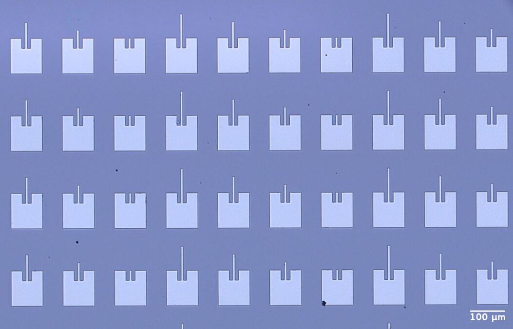
where is the free-space wave vector and is the distance between the elements. is the additional phase that comes from the direction of incidence, and in the case of broadside radiation, this term vanishes, yielding the familiar term. As the phase delay is relative, we derived a pattern that can be easily replicated across a large array. Namely, we chose to implement a radians progressive phase shift, which wraps around every four elements. The resultant direction of steering is then as per (4). The delay is implemented through a fixed-length delay stub along the resonant length of the patch. The length is calculated as per the phase constant. Namely, to effect a delay of radians, the length of the stub should be , where is the wave vector within the substrate. Based on these principles, we designed the final reflectarray as shown in Fig. 1a, where the pattern can be seen to repeat every four elements.
2.2. Fabrication
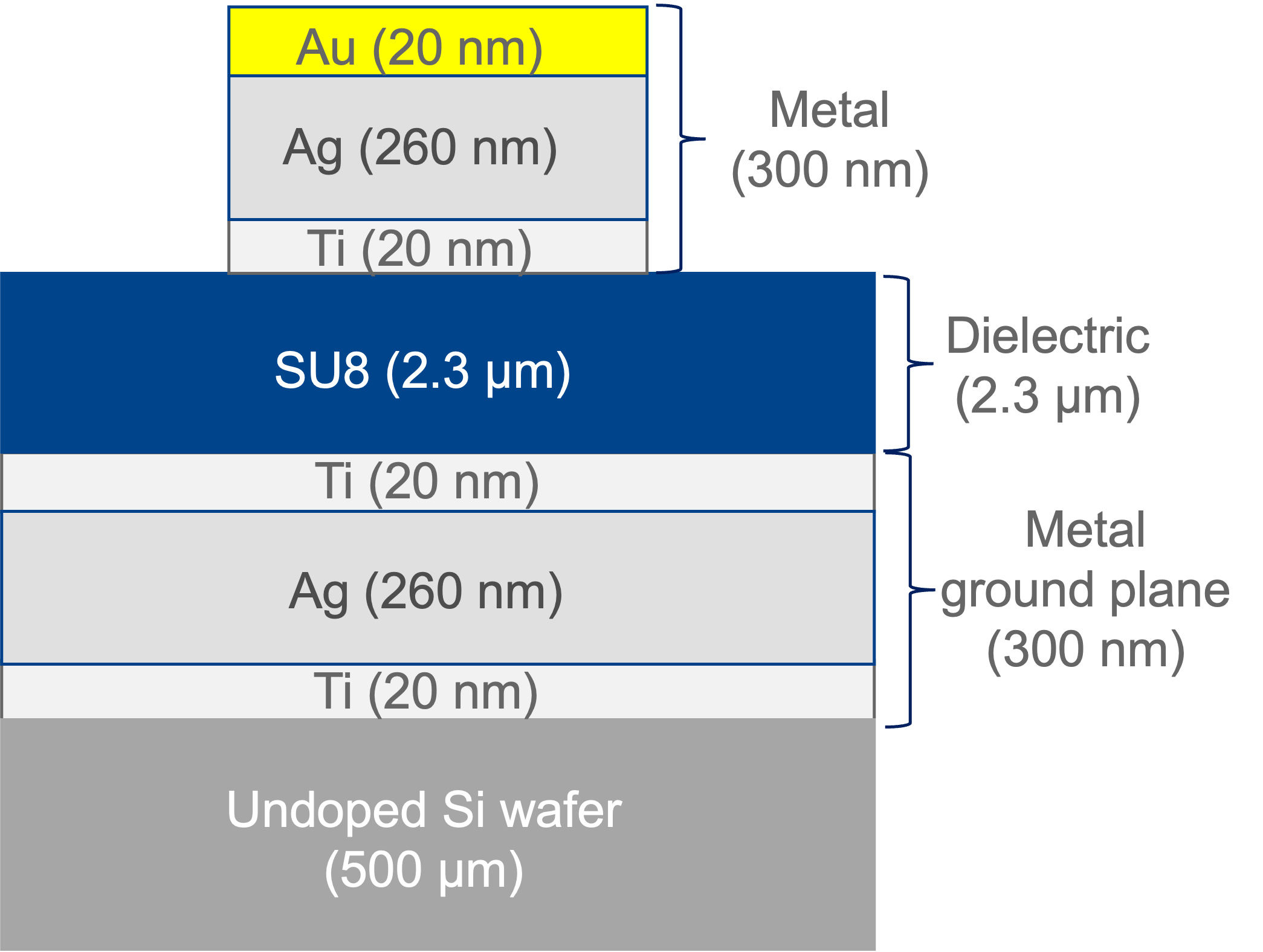
We fabricated the reflectarray on a substrate consisting of a ( Ti + Ag + Ti) metallic ground plane deposited atop a Si/SiO2 wafer to ensure high reflectivity (Abohmra et al., 2020). A SU8 layer was spin-coated on the ground plane and the reflectarray designs were patterned atop the SU8 dielectric layer using conventional photolithography.
The Si/SiO2 substrate was cleaned by sonication in acetone, isopropyl alcohol, and deionized (DI) water for each, followed by N2 blow dry and heating for at . The substrate was then treated with O2 plasma at for to remove organic contaminants. The cleaned substrate was then inserted into an electron beam evaporation system for deposition of the ground plane metals. The structure of the deposited metal (see Fig. 1b) was Ti (for adhesion), Ag (for reflection), and another Ti adhesion layer. Photolithography was used to write the array pattern onto the substrate. For improved lift-off, LOR3B photoresist was first spin coated at for , followed by a post-coat bake at for . A second photoresist (Microposit S1813) was then spin coated at for and followed by post-coat bake at for . The substrate was subsequently placed in contact with the designed photomask and exposed (Hg i-line, , ) for .
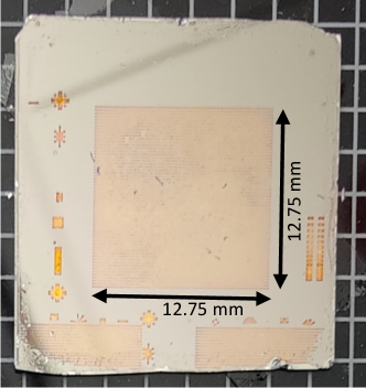
After photolithography, the photoresists were developed in Microposit MF-319 solution for followed by rinsing in DI water for . A similar metal stack ( Ti, Ag, and Au) was deposited to form the metal arrays. The topmost Au layer was deposited to prevent the Ag surface from oxidation. The sample was then left in Microposit Remover 1165 solution overnight at . After lift-off, the sample was rinsed in isopropyl alcohol (IPA) and DI water for each, followed by N2 blow dry. A photo of the resulting reflectarray is shown in Fig. 1c.
3. Experimental Validation
In this section, we validate the reflectarray working principle using two platforms, i.e., THz-TDS and a CW THz testbed.
3.1. Terahertz Time-Domain Spectroscopy
As a starting point, we used a THz-TDS platform (Advantest TAS7500TS), which offers rapid, broadband measurements in reflection or transmission (see, e.g., (Grischkowsky et al., 1990; Dai et al., 2004)). A schematic of the measurement setup (Vandrevala and Einarsson, 2019) is shown in Fig. 2.
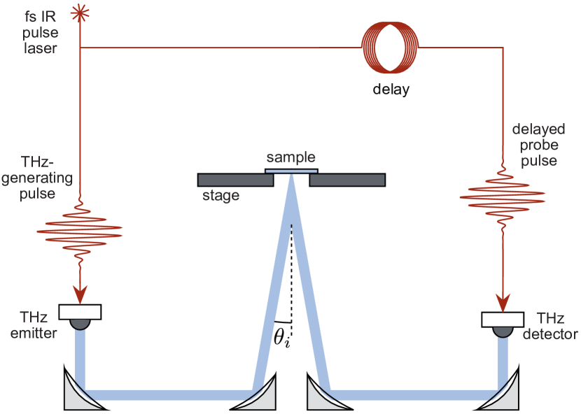
In this THz-TDS system, a femtosecond pulse from an infrared (IR) laser is incident on a photoconductive antenna, which generates a broadband THz pulse. After interacting with the sample, the THz pulse is detected at a second photoconductive antenna by mixing with a delayed IR pulse.
The non-specular reflection by the IRS should direct the component of the broadband THz pulse at the resonance frequency away from the detector, resulting in a decrease in reflectance. This can be clearly seen in the reflectance spectrum plotted in Fig. 3, where the blue curve shows a clear dip near . While designed for , the response is centered at , which is related to the tolerance in fabrication, as the stub lengths involved micrometer precision, and the photolithographic process involving complex lift-off had a tolerance of 10% ( at minimum stub length). The dashed red curve is the reflection of a uniform metal film of equal thickness, and both are normalized to the reflection from the bare substrate.

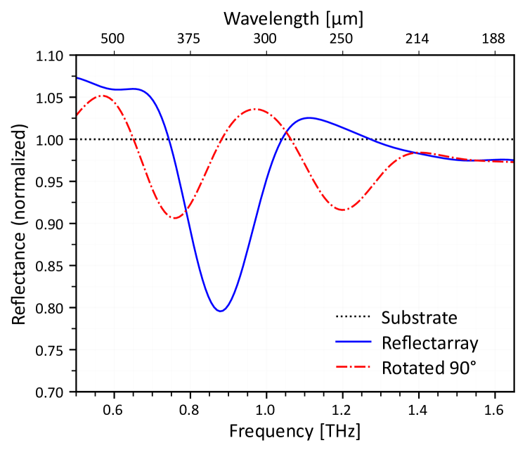
The dip at is eliminated when the sample is rotated by (Fig. 3b), confirming that the response is indeed due to the element geometry and not some other factor.
3.2. Terahertz Communication Testbed
We verify the improvement in link quality when utilizing the reflectarray through the TeraNova testbed (Sen et al., 2020).
3.2.1. Setup
The TeraNova testbed consists of a transmitter with a high-performance analog programmable signal generator (PSG) and an arbitrary waveform generator (AWG) up to 92 GSa/s from Keysight Technologies, an upconverter frontend, along with a directional high-gain horn antenna, encompassing true terahertz frequencies (). The PSG is used to generate the local oscillator (LO) signal, which is mixed with the intermediate frequency (IF) signal generated by the AWG, and finally upconverted to a higher radio frequency (RF) signal. The upconverter is manufactured by Virginia Diodes, Inc. (VDI) and consists of a frequency multiplier chain of , a frequency mixer with a double sideband (DSB) conversion loss of and an IF low-noise amplifier (LNA) with of gain. The transmit power at RF before feeding the antenna is about () and the horn antenna gain is . The testbed receiver has a similar design and is equipped with a high-performance digital storage oscilloscope (DSO) up to 160 GSa/s. The downconverter has the same architecture as the upconverter but is equipped with a high-gain IF LNA providing of gain.
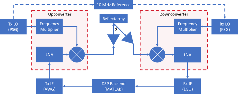
Figure 4 depicts how the different transmitter and receiver components are connected. The reference cable is used to synchronize the transmitter and receiver PSGs and compensate for the carrier frequency and phase offsets.
The digital signal processing (DSP) backend of the TeraNova testbed involves designing discrete-time pulse-shaped modulated waveforms in MATLAB and uploading them to the AWG . The AWG then generates the modulated IF signals, which are upconverted to RF by the VDI upconverters, transmitted over the air, received by the VDI downconverters, get downconverted back to IF, and are finally captured and stored via the DSO . Post-processing and DSP techniques can then be applied to the captured signals in MATLAB. Given this flexibility, we can experimentally evaluate any arbitrary modulation scheme or DSP technique.
3.2.2. Controlled Reflection Validation
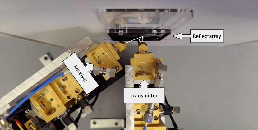
As depicted in Fig. 5, the transmitter is incident normal to the reflectarray, with the receiver placed in the direction of the controlled reflection (). We also replaced the reflectarray with a metallic sheet to act as a benchmark. As a preliminary step, we measure the signal-to-noise ratio (SNR) when utilizing the fabricated reflectarray both in the case of the receiver being placed at the expected reflection of the signal as well as specular reflection. The SNR of a IF sinusoidal signal was found to be in the controlled reflection scenario () and in the specular reflection scenario (i.e. equal incident and reflected angles from the normal). This clearly indicates that the reflectarray is working as intended and directing the radiation in a non-specular path, potentially enabling non-line-of-sight (NLoS) links.
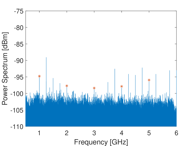
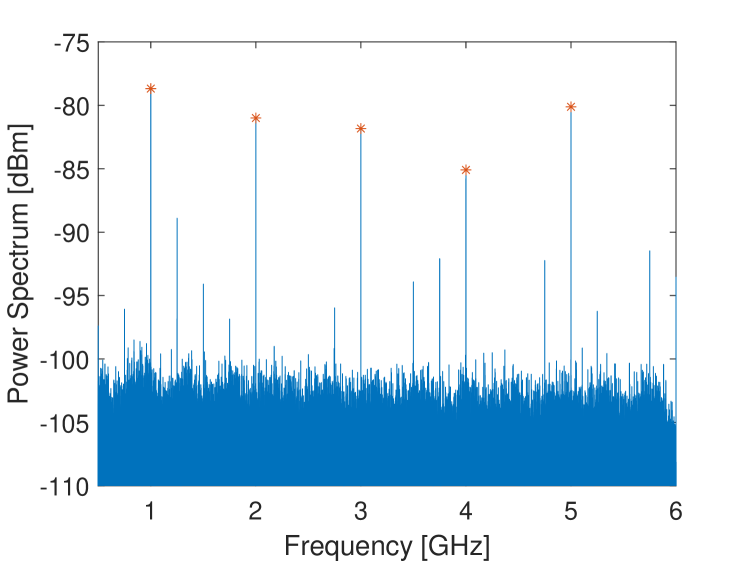
To further verify broadband operation, we upconvert and transmit an IF signal comprising the sum of five sinusoidal signals at 1, 2, 3, 4, and . These were successfully received with a high SNR, as shown in Fig. 6, in the case of the reflectarray, but the signals could not be recovered when replacing the reflectarray with a metallic sheet.
Next, we transmit a QPSK modulated data signal with a passband bandwidth of , comprising 200 pilot bits and 2000 data bits. The constellation diagram for the transmitted, received, and equalized signals is shown in Fig. 7.
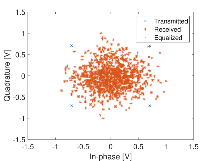
With the reflectarray, the effective received data rate was , with a measured bit error rate (BER) of 0.0335 without any error correction. This BER is very close to the theoretical additive white Gaussian noise (AWGN) channel BER given the received SNR . The measured BER when the reflectarray is replaced by a metallic sheet was 0.499, the worst possible BER . Moreover, the reflectarray can be used for multi-Gbps data rates and higher modulation orders over multi-gigahertz-wide bandwidths, but it is very challenging to close the link with sufficient SNR given the very low available transmit power at true terahertz frequencies. Nonetheless, the results verify the response of the reflectarray and the potential for establishing highly focused and even NLoS links at THz frequencies.
4. Conclusion and Future Works
In this paper, we present the first metallic reflectarray achieving NLoS communications with information-carrying signals at true terahertz frequencies. The results validate the reflectarray working principle, showing effective communication despite the very low available transmit power. In the future, we will work towards increasing the supported bandwidth and communication distance by improving the transmitter power and receiver sensitivity. We will also explore the possibility of developing tunable structures by replacing the fixed-length stubs with voltage-controlled delay lines (Singh et al., 2020a).
Acknowledgements.
This work was funded by the Air Force Research Laboratory award FA8750-20-1-0500 and the National Science Foundation awards CNS-1955004 and CNS-2011411.References
- (1)
- Abadal et al. (2020) Sergi Abadal, Chong Han, and Josep M. Jornet. 2020. Wave Propagation and Channel Modeling in Chip-Scale Wireless Communications: A Survey From Millimeter-Wave to Terahertz and Optics. IEEE Access 8 (2020), 278–293.
- Abohmra et al. (2020) Abdoalbaset Abohmra, Hassan Abbas, Muath Al-Hasan, et al. 2020. Terahertz Antenna Array Based on a Hybrid Perovskite Structure. IEEE Open Journal of Antennas and Propagation 1 (2020), 464–471.
- Akyildiz et al. (2022) Ian F. Akyildiz, Chong Han, Zhifeng Hu, Shuai Nie, and Josep M. Jornet. 2022. Terahertz Band Communication: An Old Problem Revisited and Research Directions for the Next Decade. IEEE Transactions on Communications 70, 6 (2022), 4250–4285.
- Balanis (2016) Constantine A Balanis. 2016. Antenna Theory: Analysis and Design. John Wiley & Sons.
- Dai et al. (2004) Jianming Dai, Jiangquan Zhang, Weili Zhang, et al. 2004. Terahertz time-domain spectroscopy characterization of the far-infrared absorption and index of refraction of high-resistivity, float-zone silicon. J. Opt. Soc. Am. B 21, 7 (Jul 2004), 1379–1386.
- Di Renzo et al. (2020) Marco Di Renzo, Alessio Zappone, Merouane Debbah, et al. 2020. Smart Radio Environments Empowered by Reconfigurable Intelligent Surfaces: How It Works, State of Research, and The Road Ahead. IEEE Journal on Selected Areas in Communications 38, 11 (2020), 2450–2525.
- Grischkowsky et al. (1990) D. Grischkowsky, Søren Keiding, Martin van Exter, et al. 1990. Far-infrared time-domain spectroscopy with terahertz beams of dielectrics and semiconductors. J. Opt. Soc. Am. B 7, 10 (Oct 1990), 2006–2015.
- Jornet and Sangwan (2023) Josep M. Jornet and Amit Sangwan. 2023. Nanonetworking in the Terahertz Band and Beyond. IEEE Nanotechnology Magazine 17, 3 (2023), 21–31.
- Nayeri et al. (2018) Payam Nayeri, Fan Yang, and Atef Z Elsherbeni. 2018. Reflectarray Antennas: Theory, Designs, and Applications. John Wiley & Sons.
- Niu et al. (2013) Tiaoming Niu, Withawat Withayachumnankul, Benjamin S.-Y. Ung, et al. 2013. Experimental demonstration of reflectarray antennas at terahertz frequencies. Opt. Express 21, 3 (Feb 2013), 2875–2889.
- Renzo et al. (2019) Marco Di Renzo, Merouane Debbah, Dinh-Thuy Phan-Huy, et al. 2019. Smart radio environments empowered by reconfigurable AI meta-surfaces: An idea whose time has come. EURASIP Journal on Wireless Communications and Networking 2019, 1 (2019), 1–20.
- Sen et al. (2020) Priyangshu Sen, Dimitris A. Pados, Stella N. Batalama, et al. 2020. The TeraNova platform: An integrated testbed for ultra-broadband wireless communications at true Terahertz frequencies. Computer Networks 179 (2020), 107370.
- Singh et al. (2023) Arjun Singh et al. 2023. Wavefront Engineering: Realizing Efficient Terahertz Band Communications in 6G and Beyond. IEEE Wireless Communications (to appear) (2023).
- Singh et al. (2020a) Arjun Singh, Michael Andrello, Erik Einarsson, et al. 2020a. A Hybrid Intelligent Reflecting Surface with Graphene-Based Control Elements for THz Communications. In 2020 IEEE 21st International Workshop on Signal Processing Advances in Wireless Communications (SPAWC). 1–5.
- Singh et al. (2020b) Amit Singh, Mustafa Sayginer, Michael J. Holyoak, et al. 2020b. A D-Band Radio-on-Glass Module for Spectrally-Efficient and Low-Cost Wireless Backhaul. In 2020 IEEE Radio Frequency Integrated Circuits Symposium (RFIC). 99–102.
- Vandrevala and Einarsson (2019) Farah Vandrevala and Erik Einarsson. 2019. Origin of pseudo-dispersion in non-dispersive media by terahertz time-domain spectroscopy. Opt. Express 27, 23 (Nov 2019), 33537–33542.