Equal contribution of even and odd frequency pairing to transport across normal metal-superconductor junctions
Shun Tamura1, Viktoriia Kornich1, and Björn Trauzettel1,21Institute for Theoretical Physics and Astrophysics, University of Würzburg, D-97074 Würzburg, Germany
2Würzburg-Dresden Cluster of Excellence ct.qmat, D-97074 Würzburg, Germany
Abstract
Odd-frequency pairing is an unconventional type of Cooper pairing in superconductors related to the frequency dependence of the corresponding anomalous Green function. We show by a combination of analytical and numerical methods that odd-frequency pairing is ubiquitously present in the current of Andreev-scattered particles across a junction formed by a normal metal (N) and a superconductor (S), even if the superconducting pairing is of conventional -wave, spin singlet type. We carefully analyze the conductance of NS junctions with different pairing symmetries (-wave, -wave, -wave). In all cases, we identify a generic equal balance of even and odd frequency pairing to the contributions related to Andreev reflection. This analysis shows in retrospect that the presence of odd-frequency pairing in electric currents across NS junctions is rather the rule, not the exception. This insight stems from an alternative approach of analyzing the transport problem of hybrid structures. It is based on the Kubo-Greenwood formula with direct access to symmetries of the anomalous Green functions characterizing the superconducting pairing.
We expect that our predictions substantially enrich the interpretation of transport data across NS junctions in many material combinations.
††preprint: APS/123-QED
Introduction.—
The symmetry of the superconducting pairing potential (SPP) has been the central topic since its discovery. One important (but less investigated) aspect thereof is its frequency dependence. The frequency dependence of the SPP is classified in two distinct ways: even- and odd-frequency pairing. Even-frequency pairing (EFP) applies to all known bulk superconductors to date, no matter whether their pairing is of conventional -wave, spin singlet type or unconventional. Odd-frequency pairing (OFP) is considered to be rather exotic. It refers to the property that the anomalous Green function (related to a particular type of pairing amplitude) is odd under the exchange of time or frequency [1, 2, 3, 4, 5]. Bulk OFP has not yet been discovered experimentally. In fact, its stability is an interesting research topic by itself [6, 7, 8, 9, 10]. In hybrid structures, such as normal metal (N) / superconductor (S) junctions or Josephson junctions, translation symmetry is broken. It has been soon realized that this broken symmetry gives rise to the emergence of odd-frequency pairing in superconducting hybrids [11, 12, 13, 14, 14, 14, 15, 12, 16, 17]. In Josephson junctions, supplemented with magnetic materials in the weak link, a long-range proximity effect has been considered as an indirect evidence of OFP [18]. More distinct features of OFP (as compared to EFP) have also been predicted, for instance, the paramagnetic Meissner effect, which should appear under certain conditions [19, 20, 21, 22, 23]. Indirect evidence of this particular type of attraction of magnetic flux by superconductivity has been reported in experiments based on low-energy muon spectroscopy [24, 25, 26] and on scanning tunneling spectroscopy (STS) [27, 28].
However, it is fair to say that the present-day understanding is that it is difficult to observe evidence for OFP in any type of experiment involving superconductors or hybrid junctions thereof. In this Letter, we argue that the opposite is true for standard transport measurements across NS junctions. In such junctions, it is impossible to observe genuine fingerprints of conventional EFP. In fact, we show below that the transport features related to superconductivity, i. e. Andreev reflection in the context of NS junctions, are always equally balanced by EFP and OFP contributions. This observation is deeply connected to underlying symmetries of retarded and advanced Green functions that enter into linear response expressions for the conductance. It has been overlooked so far, because common methods of calculating these transport properties do not give insight on the impact of EFP or OFP on the conductance. We benchmark our discovery by a number of examples, where the N side is either a one-dimensional (1D) system or a 1D ladder and the S side is either a 1D or a 2D superconductor with different pairing symmetries such as -wave, -wave, and -wave.
We expect that our predictions substantially enrich the interpretation of transport data across NS junctions in many material combinations
Conductance across NS junction.—
We evaluate the conductance by linear response theory employing
(1)
(2)
The spatial average is depicted by using the symbol of the over bar in this Letter:
.
Here, , is the Fermi-Dirac distribution function, , acts on , with Pauli matrices in particle-hole space, is an electron mass, is an elementary charge, and the trace is taken for particle-hole and spin space.
is given by
with the advanced (retarded) Green function (GF) .
The symbol of the over tilde is used in this way throughout this Letter.
Equation (1) in combination with Eq. (2) is known as Kubo-Greenwood formula [29, 30].
We evaluate in the N region, i.e., and are chosen in the N region.
Dividing the GFs into normal and anomalous GFs described by and , respectively, Andreev reflection is described by the anomalous part.
Then, the retarded GF can be expressed as
with
(3)
where and are normal and anomalous GF:
and
.
The advanced GF is defined similarly.
Here, is the Heisenberg representation of an annihilation operator with spin , spatial position , and time .
is a positive infinitesimal number.
can be divided into normal transmission and Andreev reflection terms:
(4)
with
and
.
There is no cross terms between normal and anomalous GFs.
Even and odd-frequency pairing contributions.—
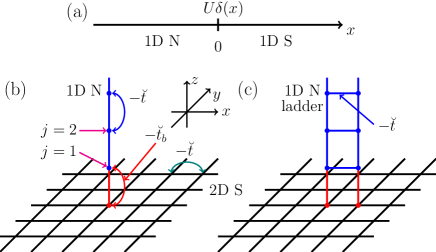
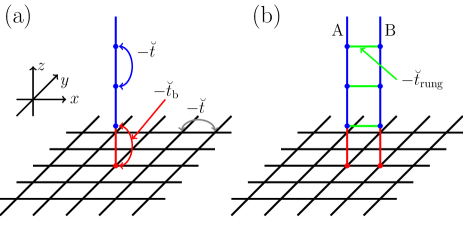
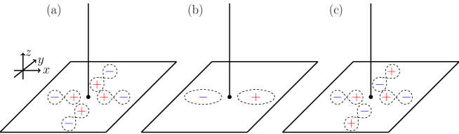
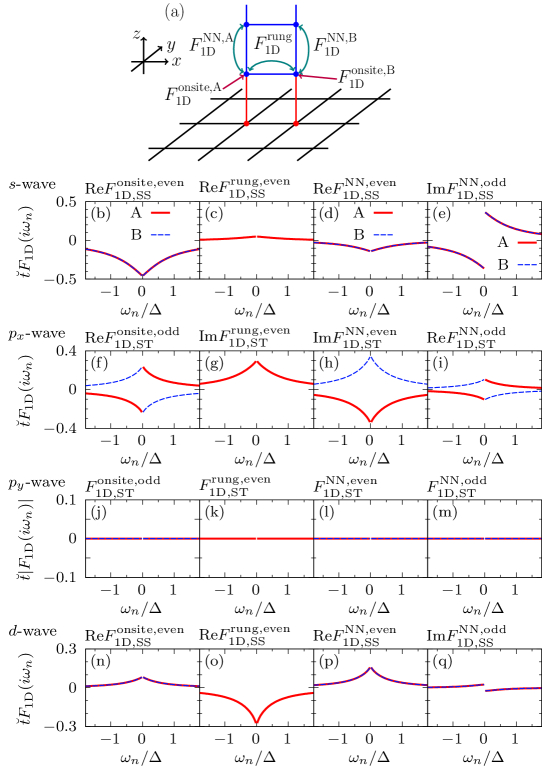
Figure 1:
Schematic illustration of three types of junctions.
(a) Continuum 1D N/1D S junction,
(b) 1D N/2D S lattice model, and
(c) 1D N ladder/2D S lattice model.
In NS junctions, OFP induced at the interface can penetrate into the N region and contribute to Andreev reflection.
We decompose into EFP and OFP components.
The advanced (retarded) GF can be written as the sum of even and odd components
.
Then, is decomposed as
with
(5)
(6)
We analyze the odd-frequency contribution to for three distinct systems illustrated in Fig. 1.
Remarkably, we demonstrate that [31].
is zero due to particle-hole symmetry [proof is given in the supplemental material (SM) [32]].
Hence, we do not discuss it.
Figure 1(a) shows the continuum 1D NS junction, where we analytically prove the equal contribution of EFP and OFP to .
Figure 1(b) shows the 1D N/2D S junction inspired by scanning tunneling spectroscopy.
In this setup, we analyze -, -, and -wave SPPs.
We demonstrate that only -wave junctions exhibit Andreev reflection since both EFP and OFP vanish at the interface between 1D N and 2D S for - and -wave junctions.
Hence, they cannot penetrate into the 1D N.
These cancellations do not occur for the setup shown in Fig. 1(c), where the normal metal has more spatial structure.
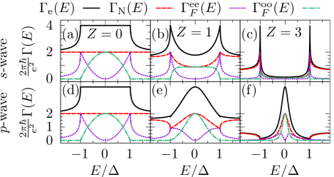
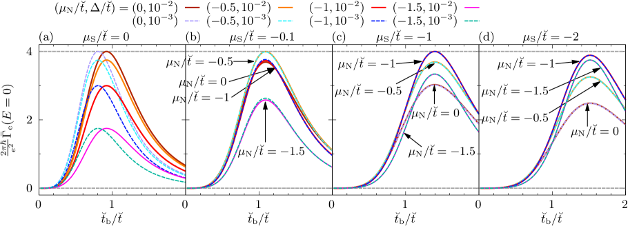
1D N/1D S continuum model.—
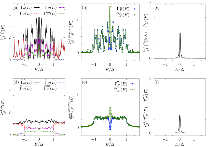
Figure 2:
and its components are plotted as a function of for several values of .
(a)–(c) -wave and (d)–(f) -wave junctions.
for (a) and (d) for (b) and (e), and for (c) and (f).
for all plots.
We now present our analytical results for the 1D N/1D S continuum model.
The Bogoliubov-de Gennes (BdG) Hamiltonian is
with , the Heaviside step function , the chemical potential, the barrier potential at the interface, and Pauli matrices in spin space.
As the SPP , we study -wave and -wave cases: for -wave, for -wave [see also Fig. 1(a)].
We define the dimensionless parameter with .
We derive the GFs along the lines of Ref. [33].
Explicit expressions are given in the SM [32].
Employing Eqs. (1) and (2), we reproduce the differential conductance of Blonder, Tinkham, and Klapwijk (BTK) theory [34, 35]: and , where the electron (hole) wave number is given by ,
and are hole (Andreev) and electron reflection coefficients, respectively.
We choose and .
The EFP and OFP contributions are
(7)
After averaging over and , the last two terms in Eq. (7) vanish.
Then, we obtain
for [36] (see the SM [32] for further details).
For the -wave junction with fully transparent barrier [ shown Fig. 2(a)],
perfect Andreev reflection occurs, and holds for [37].
As the value of increases [ and shown in Figs. 2(b) and (c), respectively], the shape of approaches the U-shaped density of states reflecting the -wave SPP.
Accordingly, the amplitude of Andreev reflection is suppressed.
For any values of , holds for due to the normalization of the coefficients: for [34].
The presence of Andreev reflection [] is, thus, inherently connected to the presence of
OFP [38, 39, 40, 41, 42, 43].
For -wave junctions [Figs. 2(d)–(f)], takes a constant value due to the presence of a Majorana state [44, 45, 46].
Half of it stems from Andreev reflection .
Experimental conductance exhibiting a zero energy peak larger than the value of the normal state signifies the existence of Andreev reflection, a distinct indicator of the presence of OFP.
Hence, in Refs. [47, 48, 49, 50, 51], signatures of OFP have been observed in retrospect.
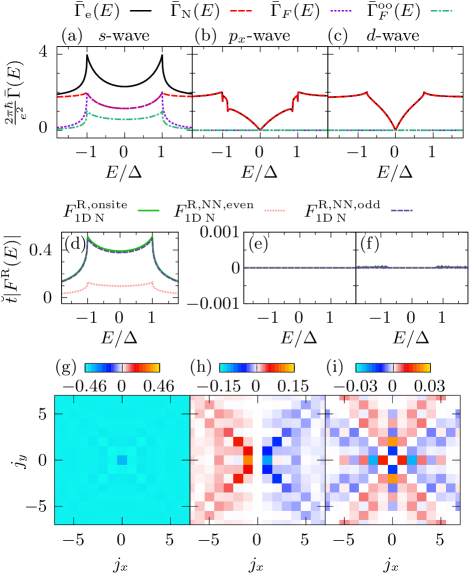
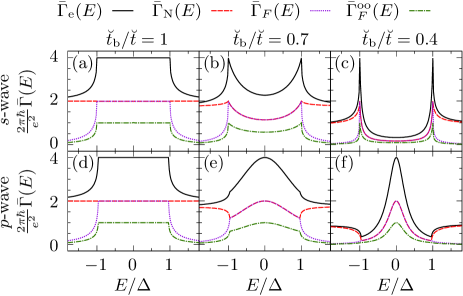
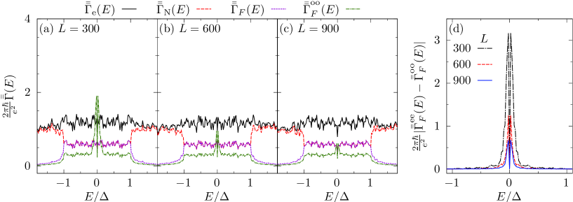
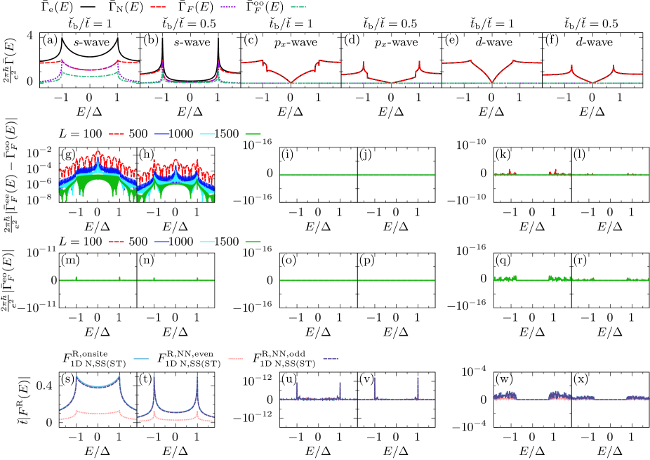
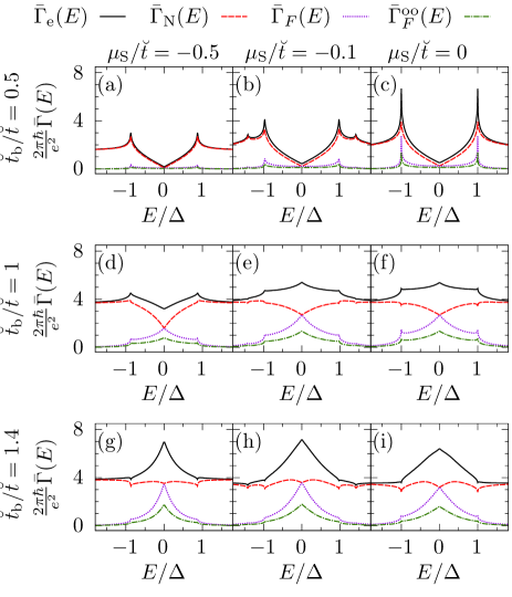
1D N/2D S lattice model.—
Figure 3:
(a)–(c) and its components are plotted as a function of .
numerically and is not plotted.
(d)–(f) The absolute value of onsite and NN retarded GF in 1d N is plotted as a function of .
(a)–(f) Averaging length , , and .
(g)–(i) Onsite component of the anomalous GF in Matsubara frequency representation in the 2D S close to the 1D N is plotted as functions of and with Matsubara frequency and .
(a), (d) and (g) -wave, (b), (e) and (h) -wave, and (c), (f) and (i) -wave S junctions.
(g) ,
(h) , and
(i) .
The imaginary part for (g)–(i) is zero.
Let us now consider the model illustrated in Fig. 1(b).
The Hamiltonian is given by
(8)
where () is an annihilation operator in 1D N (2D S) with ()-th site and spin .
Here, is a hopping integral within 1D N and 2D S, is a hopping integral between 1D N and 2D S, is a chemical potential in 1D N (2D S), and .
We utilize , , , and .
We impose periodic boundary conditions in -direction with sites and an infinite system in -direction [52].
We consider -, -, and -wave SPPs for with momentum , where is given by
,
, and
, respectively.
Without loss of generality, we assume that is real and positive.
For the lattice model, we use a discretized version of Eq. (2):
with , , , and
[53, 54].
Here, the trace in is taken for spin, particle-hole, and neighboring two spatial lattice sites spanned from to .
The spatial average is defined by with and chosen in the 1D N region.
As shown in Figs. 3(a)–(c), only the -wave junction has a non-zero Andreev reflection [].
For -wave and -wave junctions, exhibits a V-shaped structure reflecting the density of states [55, 56, 57].
Numerical equivalence of and is shown in the SM [32].
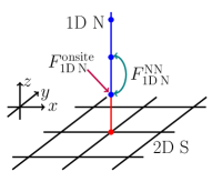
The onsite () and nearest neighbor (NN) between and components [see Fig. 1(b)] of the retarded anomalous GF in the 1D N are plotted in Figs. 3(d)–(f) [58].
In Figs. 3(d) and (f), - and -wave junctions, respectively, the spin-singlet (SS) EFP and OFP components are shown, and in Figs. 3(e), -wave junction, the spin-triplet (ST) EFP and OFP components are shown [59].
In Fig. 3(d), we confirm that EFP and OFP penetrate into 1D N [60].
For - and -wave cases, both EFP and OFP do not penetrate into 1D N [Figs.3(e) and (f)] [61].
Let us explain why EFP and OFP can (cannot) penetrate into 1D N for the -wave (- and -wave) junction.
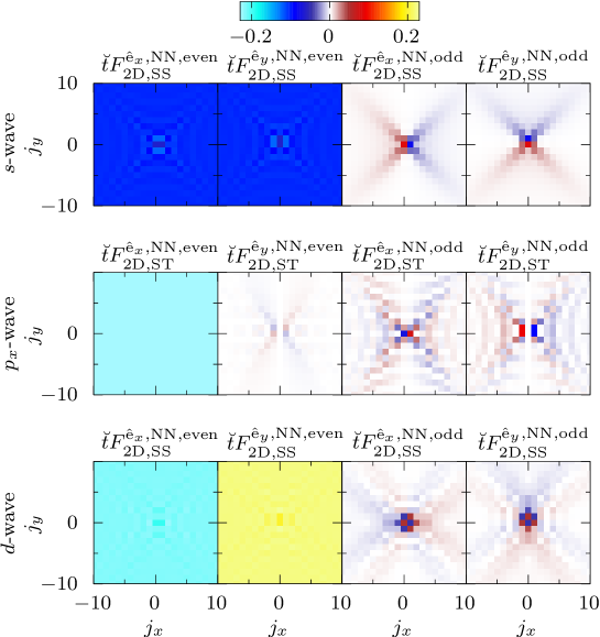
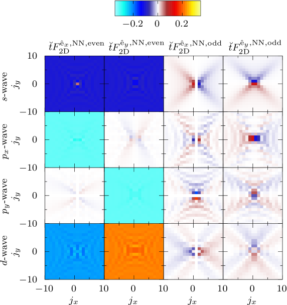
As an example, the onsite components of the anomalous GF in 2D S close to 1D N are illustrated in Figs. 3(g)–(i) (NN pairings are shown in the SM [32]).
We define the onsite SS EFP (ST OFP) component of the anomalous GF with Matsubara frequency () in 2D S as follows
(9)
with for SS EFP and for ST OFP [62].
When is non-zero, the onsite pairing can penetrate into 1D N.
For the -wave junction, the onsite anomalous GF (SS EFP) does not exhibit a sign change due to the isotropy of the -wave SPP.
Hence, this onsite pairing can penetrate into 1D N [Fig. 3(g)].
There are no cancellations for NN EFP and OFP.
Thus, they can also penetrate into 1D N [Fig. 3(d)].
For the -wave junction, the onsite anomalous GF (ST OFP) [Fig. 3(h)] exhibits a sign change at since the -wave SPP changes its sign in direction.
Then, OFPs cancel each other at and cannot penetrate into 1D N.
For the -wave S junction [Figs. 3(i)], the onsite anomalous GF (SS EFP) also exhibits a sign change at reflecting -wave symmetry.
Then, the EFP contributions cancel each other and cannot penetrate into 1D N.
For -wave and -wave junctions, NN EFP contributions also cancel each other and cannot penetrate into 1D N [32].
The same argument applies to NN OFP contributions.
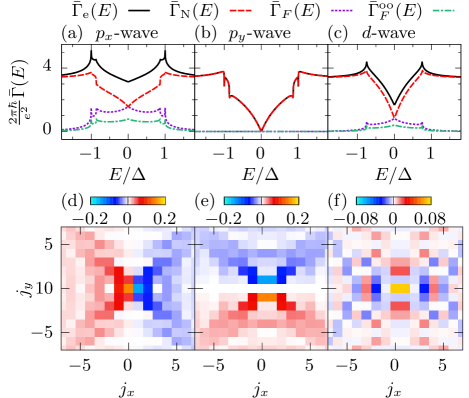
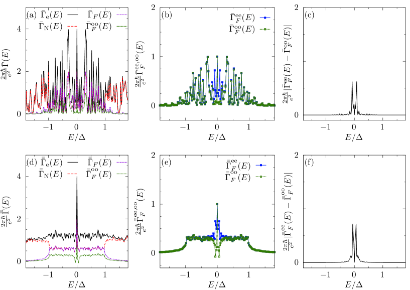
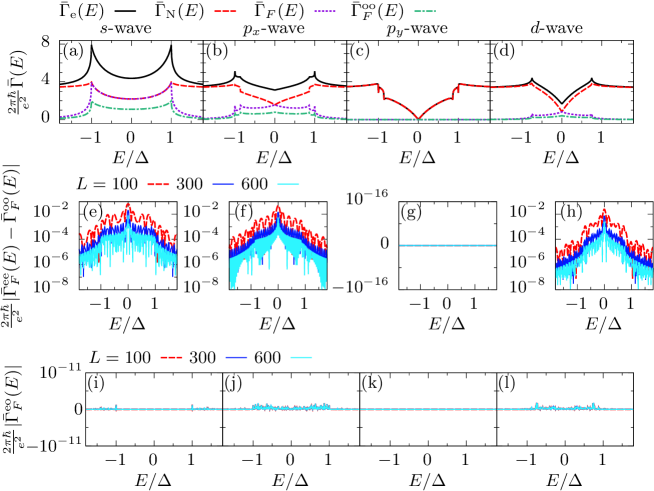
1D N ladder/2D S model.—
Figure 4:
(a)–(c) and its components are plotted as a function of with , , and .
numerically and is not plotted.
(d)–(f) Onsite component of the anomalous GF close to the 1D N ladder is plotted as functions of and at with .
(a) and (d) -wave, (b) and (e) -wave, and (c) and (f) -wave S junction.
(d) and (e) Re,
(f) Re.
The imaginary part for (d)–(f) is zero.
From the results of the 1D N/2D S junctions, we expect that EFP and OFP can penetrate into the N lead
if we replace the 1D N lead with a 1D N ladder [Fig. 1(c)].
Note that this setup mimics a double tip in STS experiments.
The 1D N ladder is connected to and .
We plot and its components in Figs. 4(a)–(c) accompanied with the onsite pairing of anomalous GFs in Figs. 4(d)–(f) for -, -, and -wave junctions.
NN pairings are shown in the SM [32].
The SPP for the -wave case is given by .
For -wave junctions, depending on the orientation of SPPs (- or -wave), EFP and OFP can penetrate into 1D N ladder.
For the -wave junction [Fig. 4(a)], we observe that EFP and OFP contribute to since onsite OFPs in the -direction do not cancel each other as shown in Fig. 4(d).
However, for the -wave junction [Fig. 4(b)], and its components are qualitatively the same as the ones in Fig. 3(b).
Then, the OFP contributions cancel each other [Fig. 4(e)] (NN EFPs and NN OFPs also cancel and cannot penetrate into 1D N ladder [32]).
For the -wave junction, shown in Fig. 4(c), EFP and OFP contribute to ,
where the EFP contributions do not cancel each other [Fig. 4(f)].
Conclusions.—
We have analyzed the impact of even- and odd-frequency pairing on the conductance across generic NS junctions based on linear response theory. We have identified an equal balance of even- and odd-frequency pairing contributions to the conductance related to Andreev reflection. The larger the transparency across the junction, the more pronounced these contributions typically are.
Hence, we prove that the presence of Andreev reflection in transport across NS junctions manifests the existence of odd-frequency pairing in a variety of hybrid structures.
We thank Y. Tanaka for helpful discussions. This work was supported by the Würzburg-Dresden Cluster of Excellence ct.qmat, EXC2147, project-id 390858490, the DFG (SFB 1170), and the Bavarian Ministry of Economic Affairs, Regional Development and Energy within the High-Tech Agenda Project “Bausteine für das Quanten Computing auf Basis topologischer Materialen”.
References
Berezinskii [1974]V. L. Berezinskii, New model of the anisotropic phase of superfluid He3, JETP Lett. 20, 287 (1974).
Triola et al. [2020]C. Triola, J. Cayao, and A. M. Black-Schaffer, The role of odd-frequency pairing in multiband superconductors, Annalen der Physik 532, 1900298 (2020).
Kirkpatrick and Belitz [1991]T. R. Kirkpatrick and D. Belitz, Disorder-induced triplet superconductivity, Phys. Rev. Lett. 66, 1533 (1991).
Balatsky and Abrahams [1992]A. Balatsky and E. Abrahams, New class of singlet superconductors which break the time reversal and parity, Phys. Rev. B 45, 13125 (1992).
Emery and Kivelson [1992]V. J. Emery and S. Kivelson, Mapping of the two-channel Kondo problem to a resonant-level model, Phys. Rev. B 46, 10812 (1992).
Hoshino et al. [2011]S. Hoshino, J. Otsuki, and Y. Kuramoto, Diagonal Composite Order in a Two-Channel Kondo Lattice, Phys. Rev. Lett. 107, 247202 (2011).
Bergeret et al. [2001]F. S. Bergeret, A. F. Volkov, and K. B. Efetov, Long-Range Proximity Effects in Superconductor-Ferromagnet Structures, Phys. Rev. Lett. 86, 4096 (2001).
Tanaka and Kashiwaya [2004]Y. Tanaka and S. Kashiwaya, Anomalous charge transport in triplet superconductor junctions, Phys. Rev. B 70, 012507 (2004).
Bergeret et al. [2005]F. S. Bergeret, A. F. Volkov, and K. B. Efetov, Odd triplet superconductivity and related phenomena in superconductor-ferromagnet structures, Rev. Mod. Phys. 77, 1321 (2005).
Tanaka et al. [2007]Y. Tanaka, Y. Tanuma, and A. A. Golubov, Odd-frequency pairing in normal-metal/superconductor junctions, Phys. Rev. B 76, 054522 (2007).
Tanaka and Golubov [2007]Y. Tanaka and A. A. Golubov, Theory of the proximity effect in junctions with unconventional superconductors, Phys. Rev. Lett. 98, 037003 (2007).
Asano and Tanaka [2013]Y. Asano and Y. Tanaka, Majorana fermions and odd-frequency Cooper pairs in a normal-metal nanowire proximity-coupled to a topological superconductor, Phys. Rev. B 87, 104513 (2013).
Löthman et al. [2021]T. Löthman, C. Triola, J. Cayao, and A. M. Black-Schaffer, Disorder-robust -wave pairing with odd-frequency dependence in normal metal–conventional superconductor junctions, Phys. Rev. B 104, 094503 (2021).
Khaire et al. [2010]T. S. Khaire, M. A. Khasawneh, W. P. Pratt, and N. O. Birge, Observation of Spin-Triplet Superconductivity in Co-Based Josephson Junctions, Phys. Rev. Lett. 104, 137002 (2010).
Abrahams et al. [1995]E. Abrahams, A. Balatsky, D. J. Scalapino, and J. R. Schrieffer, Properties of odd-gap superconductors, Phys. Rev. B 52, 1271 (1995).
Suzuki and Asano [2014]S.-I. Suzuki and Y. Asano, Paramagnetic instability of small topological superconductors, Phys. Rev. B 89, 184508 (2014).
Lee et al. [2017]S.-P. Lee, R. M. Lutchyn, and J. Maciejko, Odd-frequency superconductivity in a nanowire coupled to Majorana zero modes, Phys. Rev. B 95, 184506 (2017).
Parhizgar and Black-Schaffer [2021]F. Parhizgar and A. M. Black-Schaffer, Diamagnetic and paramagnetic Meissner effect from odd-frequency pairing in multiorbital superconductors, Phys. Rev. B 104, 054507 (2021).
Di Bernardo et al. [2015]A. Di Bernardo, Z. Salman, X. L. Wang, M. Amado, M. Egilmez, M. G. Flokstra, A. Suter, S. L. Lee, J. H. Zhao, T. Prokscha, E. Morenzoni, M. G. Blamire, J. Linder, and J. W. A. Robinson, Intrinsic Paramagnetic Meissner Effect Due to
-Wave Odd-Frequency Superconductivity, Phys. Rev. X 5, 041021 (2015).
Krieger et al. [2020]J. A. Krieger, A. Pertsova, S. R. Giblin, M. Döbeli, T. Prokscha, C. W. Schneider, A. Suter, T. Hesjedal, A. V. Balatsky, and Z. Salman, Proximity-Induced Odd-Frequency Superconductivity in a Topological Insulator, Phys. Rev. Lett. 125, 026802 (2020).
Alpern et al. [2021]H. Alpern, M. Amundsen, R. Hartmann, N. Sukenik, A. Spuri, S. Yochelis, T. Prokscha, V. Gutkin, Y. Anahory, E. Scheer, J. Linder, Z. Salman, O. Millo, Y. Paltiel, and A. Di Bernardo, Unconventional meissner screening induced by chiral molecules in a conventional superconductor, Phys. Rev. Mater. 5, 114801 (2021).
Perrin et al. [2020]V. Perrin, F. L. N. Santos, G. C. Ménard, C. Brun, T. Cren, M. Civelli, and P. Simon, Unveiling odd-frequency pairing around a magnetic impurity in a superconductor, Phys. Rev. Lett. 125, 117003 (2020).
van Weerdenburg et al. [2023]W. M. J. van Weerdenburg, A. Kamlapure, E. H. Fyhn, X. Huang, N. P. E. van Mullekom, M. Steinbrecher, P. Krogstrup, J. Linder, and A. A. Khajetoorians, Extreme enhancement of superconductivity in epitaxial aluminum near the monolayer limit, Science Advances 9, eadf5500 (2023).
Baranger and Stone [1989]H. U. Baranger and A. D. Stone, Electrical linear-response theory in an arbitrary magnetic field: A new Fermi-surface formation, Phys. Rev. B 40, 8169 (1989).
[31], , and do not depend on , and due to current conservation. However, , and depend on and , and spatial averaging is needed.
[32]See Supplemental Material.
McMillan [1968]W. L. McMillan, Theory of Superconductor—Normal-Metal Interfaces, Phys. Rev. 175, 559 (1968).
Blonder et al. [1982]G. E. Blonder, M. Tinkham, and T. M. Klapwijk, Transition from metallic to tunneling regimes in superconducting microconstrictions: Excess current, charge imbalance, and supercurrent conversion, Phys. Rev. B 25, 4515 (1982).
[36]At , the particle and hole momentum coincide (), and the decompositon into EFP and OFP is not unique. On the other hand, for , the decomposition is unique.
[37]With an approximation , is exactly for , but without this approximation, it is not exactly , where for when .
Lee et al. [2019]S. Lee, V. Stanev, X. Zhang, D. Stasak, J. Flowers, J. S. Higgins, S. Dai, T. Blum, X. Pan, V. M. Yakovenko, J. Paglione, R. L. Greene, V. Galitski, and I. Takeuchi, Perfect Andreev reflection due to the Klein paradox in a topological
superconducting state, Nature 570, 344 (2019).
Parab et al. [2019]P. Parab, D. Singh, S. Haram, R. P. Singh, and S. Bose, Point contact Andreev reflection studies of a non-centro symmetric superconductor Re6Zr, Scientific Reports 9, 2498 (2019).
Soulen et al. [1998]R. J. Soulen, J. M. Byers, M. S. Osofsky, B. Nadgorny, T. Ambrose, S. F. Cheng, P. R. Broussard, C. T. Tanaka, J. Nowak, J. S. Moodera, A. Barry, and J. M. D. Coey, Measuring the Spin Polarization of a Metal with a Superconducting Point Contact, Science 282, 85 (1998).
Zareapour et al. [2017]P. Zareapour, A. Hayat, S. Y. F. Zhao, M. Kreshchuk, Z. Xu, T. S. Liu, G. D. Gu, S. Jia, R. J. Cava, H.-Y. Yang, Y. Ran, and K. S. Burch, Andreev reflection without Fermi surface alignment in high- van der Waals heterostructures, New Journal of Physics 19, 043026 (2017).
Voerman et al. [2019]J. A. Voerman, J. C. de Boer, T. Hashimoto, Y. Huang, C. Li, and A. Brinkman, Dominant -wave superconducting gap in observed by tunneling spectroscopy on side junctions, Phys. Rev. B 99, 014510 (2019).
Hwang et al. [2015]I. Hwang, K. Lee, H. Jin, S. Choi, E. Jung, B. H. Park, and S. Lee, A new simple method for point contact Andreev reflection (PCAR) using a self-aligned atomic filament in transition-metal oxides, Nanoscale 7, 8531 (2015).
Tamura et al. [2020]S. Tamura, S. Nakosai, A. M. Black-Schaffer, Y. Tanaka, and J. Cayao, Bulk odd-frequency pairing in the superconducting su-schrieffer-heeger model, Phys. Rev. B 101, 214507 (2020).
Kuzmanovski et al. [2020]D. Kuzmanovski, A. M. Black-Schaffer, and J. Cayao, Suppression of odd-frequency pairing by phase disorder in a nanowire coupled to majorana zero modes, Phys. Rev. B 101, 094506 (2020).
Mourik et al. [2012]V. Mourik, K. Zuo, S. M. Frolov, S. R. Plissard, E. P. A. M. Bakkers, and L. P. Kouwenhoven, Signatures of Majorana Fermions in Hybrid Superconductor-Semiconductor Nanowire Devices, Science 336, 1003 (2012).
Xu et al. [2015]J.-P. Xu, M.-X. Wang, Z. L. Liu, J.-F. Ge, X. Yang, C. Liu, Z. A. Xu, D. Guan, C. L. Gao, D. Qian, Y. Liu, Q.-H. Wang, F.-C. Zhang, Q.-K. Xue, and J.-F. Jia, Experimental Detection of
a Majorana Mode in the core of a Magnetic Vortex inside a Topological Insulator-Superconductor Heterostructure, Phys. Rev. Lett. 114, 017001 (2015).
Sun et al. [2016]H.-H. Sun, K.-W. Zhang, L.-H. Hu, C. Li, G.-Y. Wang, H.-Y. Ma, Z.-A. Xu, C.-L. Gao, D.-D. Guan, Y.-Y. Li, C. Liu, D. Qian, Y. Zhou, L. Fu, S.-C. Li, F.-C. Zhang, and J.-F. Jia, Majorana Zero Mode Detected with Spin Selective Andreev Reflection in the Vortex of a Topological Superconductor, Phys. Rev. Lett. 116, 257003 (2016).
Heedt et al. [2021]S. Heedt, M. Quintero-Pérez, F. Borsoi, A. Fursina, N. van Loo, G. P. Mazur, M. P. Nowak, M. Ammerlaan, K. Li, S. Korneychuk, J. Shen, M. A. Y. van de Poll, G. Badawy, S. Gazibegovic, N. de Jong, P. Aseev, K. van Hoogdalem, E. P. A. M. Bakkers, and L. P. Kouwenhoven, Shadow-wall lithography of ballistic superconductor–semiconductor quantum devices, Nature Communications 12, 4914 (2021).
[52]We utilize the recursive Green function method [63] to calculate the Green function. Then, the system can be infinite in one direction, but we must impose periodic or open boundary conditions in other directions.
Fisher and Lee [1981]D. S. Fisher and P. A. Lee, Relation between conductivity and transmission matrix, Phys. Rev. B 23, 6851 (1981).
Pan et al. [2001]S. H. Pan, J. P. O’Neal, R. L. Badzey, C. Chamon, H. Ding, J. R. Engelbrecht, Z. Wang, H. Eisaki, S. Uchida, A. K. Gupta, K.-W. Ng, E. W. Hudson, K. M. Lang, and J. C. Davis, Microscopic electronic inhomogeneity in the
high- superconductor Bi2Sr2CaCu2O8+x, Nature 413, 282 (2001).
Fischer et al. [2007]O. Fischer, M. Kugler, I. Maggio-Aprile, C. Berthod, and C. Renner, Scanning tunneling spectroscopy of high-temperature superconductors, Rev. Mod. Phys. 79, 353 (2007).
Fujita et al. [2012]K. Fujita, A. R. Schmidt, E.-A. Kim, M. J. Lawler, D. Hai Lee, J. C. Davis, H. Eisaki, and S.-i. Uchida, Spectroscopic Imaging Scanning Tunneling Microscopy Studies of Electronic Structure in the Superconducting and Pseudogap Phases of Cuprate High- Superconductors, Journal of the Physical Society of Japan 81, 011005 (2012).
[58]In Figs. 3(d)–(f), and are defined as follows. For - and -wave junctions, the onsite component is SS -wave EFP:
(10)
and the NN components are SS -wave EFP and SS -wave OFP:
(11)
For –wave junctions, the onsite component is ST -wave OFP:
(12)
and the NN components are ST -wave EFP and ST -wave OFP:
(13)
.
[59]Due to spin rotational symmetry, -wave and -wave junctions can only have SS components, and -wave S junctions can only have ST components. For onsite pairings, the SS OFP is forbidden by Fermi-Dirac statistics.
[60]The EFP and OFP components of retarded GFs are not even and odd function of , respectively. EFP and OFP satisfy and , respectively.
[61]The numerical error for -wave junctions is larger than that for -wave junctions since EFP and OFP contributions between - and -direction cancel each other for -wave junctions. We adopt periodic boundary conditions in -direction and infinite length in -direction. When the system size in -direction is finite, there is no perfect cancelation in and -direction [Fig. 3(f)]. However, for -wave junctions, EFP and OFP in - and -direction cancel. Hence, in this case, there is almost no finite size effect [Fig. 3(e)].
[62]We use the Matsubara frequency representation to reduce finite-size effects. To calculate the GF in real space, we cannot access large due to the limitation of numerical resources. For finite , the finite size effects of the GF reduce when we adopt Matsubara frequency representation for not too small Matsubara frequency.
Supplemental Material: Equal contribution of even and odd frequency pairing to transport across normal metal-superconductor junctions
S1 Continuum models
S1.1 Conductance in 1D continuum model
In linear response theory, the conductance given between two points in space and is written in the form
(S1)
(S2)
with
(S3)
(S4)
(S5)
(S6)
(S7)
for continuum systems with Pauli matrices acting on particle-hole space.
Here, and are chosen in the normal metal region since the charge current is not conserved in the superconducting region.
is the advanced (retarded) Green function, with a positive infinitesimal number ,
acts on , in Eq. (S3) is taken for inner degrees of freedom e.g., spin and orbital, and is the Fermi-Dirac distribution function.
is an inner degree of freedom. Any choice of results in the same due to the following relation:
(S8)
for .
Equation (S1) in combination with Eqs. (S2), (S3), (S5), and (S6) with is called the Kubo-Greenwood formula [29, 30].
For , Eqs. (S5) and (S6) with reduces to
(S9)
which is called Caroli formula [64].
Due to the charge current conservation, Eq. (S2) can be recast into the form
(S10)
where the right hand side of Eq. (S10) does not depend on the positions and [30, 53, 54].
We assume one dimensional conductors in Eq. (S2), but extensions to higher dimensions are straightforward.
We set unless it is specified otherwise since numerical errors become smallest at with .
S1.2 Odd frequency pairing
Odd-frequency pairing is described by the anomalous Green function in superconductor junctions.
The full Green function is given by
(S11)
where
with T indicating the transpose of a vector, positive imaginary time , and the expectation value taken at temperature .
The Matsubara frequency representation of this Green function is given by
(S12)
(S13)
has four components, which we denote as
(S14)
(S15)
(S16)
(S17)
Equations (S16) and (S17) are called anomalous Green functions.
Let and be
(S18)
(S19)
We define even (odd) frequency components thereof by
(S20)
Evidently, is an even (odd) function of .
Making use of an analytic continuation, with , we can extend the definition of the Green function to the complex plain: .
From Eqs. (S18) and (S19), the Green function with complex frequency can be written as
(S21)
Then, advanced (retarded) Green function can be obtained by with positive infinitesimal number .
Likewise, we obtain advanced even (odd) frequency anomalous Green function and retarded one .
S1.3 Decomposition of
From Eq. (S21), we can write the advanced (retarded) Green function as
(S22)
(S23)
(S24)
where denotes the normal Green function and the anomalous Green function.
We can also decompose and given by Eqs. (S5) and (S6), respectively, as in the same manner.
Then, Eq. (S2) can be written as
(S25)
(S26)
(S27)
Next, we further decompose into two parts with
(S28)
(S29)
and define and in a similar manner as Eqs. (S5) and (S6), respectively, by using Eqs. (S28) and (S29).
Making use of Eqs. (S28) and (S29), Eq. (S27) can be rewritten as
(S30)
with
(S31)
(S32)
Generally, each term on the right hand side of Eq. (S29) depends on and although the left hand side of Eq. (S30) is independent of and .
It is noted that there are two types current conservation in the N region: charge and particle current conservation.
Similar to Eq. (S3), the differential conductance for the particle current is given by .
Both and do not depend on the positions and . Therefore, and also do not depend on and .
However, generally depends on and .
The cross term between even and odd-frequency, , is zero due to particle-hole symmetry.
The anomalous Green function satisfies the following relations according to the definitions Eqs. (S13), (S16), and (S17).
The component of the differential conductance for the cross term between even and odd-frequency pairing satisfies
(S39)
Particle-hole symmetry of the Hamiltonian gives
(S40)
(S41)
where the charge conjugation operator is given by , is a complex conjugation operator, is a normal part of the Hamiltonian, and is a superconducting pair potential ().
The Green function satisfies
(S42)
Then, satisfies
(S43)
where we used the relation and .
Hence, after averaging over and , we obtain
We can calculate the conductance for NS junctions by utilizing the Blonder, Tinkham, and Klapwijk (BTK) approach [34].
In this subsection, we explain the BTK approach for the calculation of the conductance across NS junctions.
For the S side, we take two prominent examples: -wave spin-singlet and -wave spin-triplet.
In general, Bogoliubov-de Gennes (BdG) Hamiltonian is given by
(S45)
(S46)
with .
Let us consider a 1D normal metal () superconductor () junction.
As a normal part of the Hamiltonian, , we consider following function:
(S47)
where is a mass of electron, is a chemical potential, and is a barrier potential at the interface.
As a pair potential, we consider an -wave spin-singlet and -wave spin-triplet.
For the -wave spin-singlet case, the pair potential is given by with the Heaviside step function and .
For the -wave spin-singlet case, we adopt .
In momentum space, the pair potential for the -wave S is given by with the signum function .
We can divide the BdG Hamiltonian into two disconnected parts with basis and , respectively.
Then, if we choose the basis , the Hamiltonian can be reduced to a matrix:
(S48)
(S49)
with Pauli matrices acting on particle-hole space.
In this approach, we first write down the scattering states in N and S regions at a given energy :
(S50)
(S51)
with
(S52)
(S53)
(S54)
(S55)
(S56)
(S57)
with for the -wave pair potential, and for the -wave pair potential.
We approximate the wave vector with the Fermi momentum assuming that the Fermi energy satisfies and .
From Eqs. (S54) and (S55), we obtain
(S58)
(S59)
Next, we solve the boundary conditions at :
(S60)
(S61)
These boundary conditions imply
(S62)
(S63)
(S64)
(S65)
(S66)
Finally, the conductance is given by
(S67)
(S68)
When , coefficients and satisfy , and Eq. (S68) can be recast as
(S69)
We obtain the same results if we choose the basis .
The total differential conductance is given by the sum of the two channels.
S1.5 Green function in continuum system
We explain how to derive the Green function in the continuum NS junction (McMillan’s method [33]).
The BdG Hamiltonian is given by Eqs. (S48) and (S49)
with basis .
We can repeat the same procedure for the basis and we obtain the same differential conductance.
We suppose .
To calculate the retarded Green function, we consider the following wave functions.
The wave functions for at complex energy () can be written as
(S70)
(S71)
(S72)
(S73)
and likewise, for ,
(S74)
(S75)
(S76)
(S77)
with
(S78)
(S79)
Here,
, and .
and
satisfy
(S80)
(S81)
(S82)
(S83)
(S84)
(S85)
The coefficients , and are determined by
the boundary conditions at :
(S86)
(S87)
with a positive infinitesimal number .
The solutions for and are lengthy expressions.
We only display the results for below.
The retarded Green function is given by
(S88)
In this equation, we take the limit .
The arrows in Eqs. (S70)–(S77) stand for asymptotic states
.
In the opposite limit, they diverge.
Hence, Eq. (S88) converges in both limit and .
It is noted that we assume that the S pair potential is real, and the Green function is given by Eq. (S88).
The retarded Green function satisfies .
The coefficients and are determined by the boundary conditions
(S89)
(S90)
The obtained results are
(S91)
Then, the retarded Green function for can be written as
(S92)
where the coefficients , , , and are given by
(S93)
(S94)
(S95)
(S96)
The advanced Green function can be determined by .
From Eqs. (S2) and (S3), we obtain
(S97)
(S98)
(S99)
Applying Andreev approximation, i.e., , we obtain the differential conductance of the BTK approach given by Eq. (S68) with the BTK’s notation and .
It is noted that when we average over and according to Eq. (S2), the contribution from is not relevant for sufficiently large value of , where the derivative of the Green function is not well defined at .
Therefore, we can neglect the contribution from .
(S100)
(S101)
After spatial averaging, we obtain
(S102)
Note that terms depending on and vanish for .
Then, the final result reads
(S103)
(S104)
for .
For , holds, and we obtain and
(S105)
Here, the angle appears as introduced in Eqs. (S5) and (S6).
Equation (S105) indicate that the decomposition into even and odd-frequency contributions at is not unique.
Note that this angle does not affect the total conductance measured in the laboratory.
Here, we show the differential conductance and its components for the basis . By utilizing the basis , we obtain exactly the same differential conductance. Hence, the total differential conductance and its components are given by the twice of Eqs. (S97)-(S105).
S1.6 Approximation for momentum and
For and , we can approximate the wave numbers as .
, , , and can be written as
(S106)
(S107)
(S108)
(S109)
The coefficient for the -wave junction is given by
(S110)
and, for the -wave junction, it becomes
(S111)
For both - and -wave junctions, from Eqs. (S110) and (S111), we obtain
(S112)
Then, the contribution of the anomalous Green function to for the -wave case is
(S113)
for .
Likewise, for the -wave case, the components of are
(S114)
for .
For the -wave case, the limit irrespective of the value of due to the presence of a Majorana state.
S2 Lattice models
S2.1 1D N/1D S junction on lattice
To compare our results between 1D continuum model and 1D lattice model, we first present the results about 1D N/1D S junctions derived on the lattice.
The mean-field Hamiltonian is given by
(S115)
(S116)
(S117)
(S118)
with for the -wave junction.
Here, the hopping integral in 1D N and 1D S, the hopping integral between 1D N and 1D S, the chemical potential, and the superconducting pair potential.
S2.2 Conductance in lattice model
in the lattice model is given by
(S119)
with the current operator on the 1D N side
(S120)
(S121)
(S122)
(S123)
where is the spatial position of the -th lattice site.
and are given by
(S124)
(S125)
(S126)
Note that we introduce the same angle as in Eqs. (S5) and (S6) in the continuum case.
In the main text, we use for 1D N (ladder)/2D S junctions since the numerical convergence is the fastest.
Here, let us show for the lattice model.
The BdG Hamiltonian has particle-hole symmetry:
(S128)
(S129)
(S130)
with complex conjugation operator .
The Green function () satisfies and .
(S131)
(S132)
(S133)
(S134)
(S135)
with ,
,
,
,
, and .
The cross term between even and odd frequency pairing for the differential conductance satisfies
(S136)
Here, we use the relation .
Also, from particle-hole symmetry, satisfies
(S137)
with .
After averaging over and of Eqs. (S136) and (S137), we obtain .
S2.3 and odd-frequency pairing
The components of for the -wave junction are shown in Figs. S1(a)–(c).
The qualitative results are the same as those in the continuum model.
We attribute all differences to finite-size effects.
In Fig. S1(a), at is almost (the maximum value).
At , we can analytically obtain the condition of for the -wave junction, which is given by
.
Figures S1(d)–(f) show and its components for the -wave junction.
At , holds due to the presence of the Majorana state independent of the value of since the chemical potential resides in the topological regime.
Figure S1:
, , , and are plotted as a function of for , , and with , , , and .
(a)–(c) 1D N/1D -wave junctions, and (d)–(f) 1D N/1D -wave junctions.
Figure S2: The anomalous Green function on the 1D N side is plotted as a function of . (a)–(c) spin-singlet components of -wave junctions, (d)–(e) spin-triplet components of -wave junctions.
(a) Real part of onsite component, (b) real part of the NN even-frequency component, (c) imaginary part of the NN odd-frequency components.
(d) Real part of onsite component, (e) imaginary part of the NN even-frequency component, (f) real part of the NN odd-frequency components.
for the -wave junction.
for the -wave junction.
and .
In Fig. S2, the anomalous Green function as a function of the Matsubara frequency in 1D N is shown.
The onsite and nearest neighbor (NN) spin-singlet (SS) and spin-triplet (ST) components are given by
(S138)
(S139)
with for the SS case, for the ST case, for the even frequency pair, and for the odd frequency pair.
In Figs. S2(a)–(c), anomalous Green functions for -wave junctions are shown.
Figures. S2(a) and (b) display the even frequency components.
Both of them have non-zero values.
Fig. S2(c) displays the NN component of odd-frequency pairing.
Note that has jump at .
This jump significantly contributes to .
Figures S2(d)–(f) show the anomalous Green functions for -wave junctions.
Figures. S2(d) and (f) are the corresponding odd-frequency components.
These components (with ) contribute to .
Due to the presence of the Majorana state, the odd-frequency component of is independent of .
Additionally, the even-frequency component of the anomalous Green function [Fig. S2(e)] with is independent of .
In Fig. S3, we show and dependence of and for -wave junctions.
The numerical convergence of is the fastest for and .
For the continuum model, in Eq. (S100), the first term, which has longer spatial oscillation period compared with the second term, is zero for and .
This indicates that at or , the slowly varying term also vanishes in lattice models, which might be the reason that the numerical convergence is the fastest.
is zero within numerical errors.
For -wave junctions shown in Figs. S4, the numerical convergence of is also the fastest for and .
is also zero within numerical error.
We conclude that average values do not depend on for a sufficiently large averaging length .
Figure S3:
and dependence of and are plotted as a function of for 1D lattice -wave junctions.
, , , and .
Figure S4:
Size and dependence of and are plotted as a function of for 1D lattice -wave junctions.
, , , and .
S2.4 and dependence of and
Figure S5:
, , , , , and are plotted as functions of and for 1D N/1D -wave junction with , , , , , , , , , and .
Figure S6:
, , , , , and are plotted as functions of and for 1D N/1D -wave junction with , , , , , , , , , and .
We discuss the positional dependence of for the 1D N/1D S junction.
In this section, we adopt .
We fix and study the dependence of the components of .
Figures S5 and S6 display and its components for the 1D N/1D -wave and 1D N/1D -wave junction, respectively.
As discussed in Sec. S1.3, , , and are independent of and .
In -wave and -wave junctions, holds.
We see that and have a finite dependence.
From Figs. S5 and S6, we observe that the spatial dependence of is smaller for smaller ().
When becomes larger (), changes rapidly as a function of .
These results indicate that the oscillation period is determined by the superconducting coherence length.
Figure S7:
, , , , , and are plotted as functions of and for 1D N/1D -wave junction with , , , , , , , , , and .
Figure S8:
, , , , , and are plotted as functions of and for 1D N/1D -wave junction with , , , , , , , , , and .
Figures S7 and S8 show and its components for the 1D N/1D -wave and 1D N/1D -wave junction, respectively.
In these figures, we can see that the qualitative behaviors are the same as Figs. S5 and S6, respectively.
S2.5 Robustness of against disorder
Here, we show that holds in the presence of disorder by numerical calculation.
We consider two types of disordered 1D junctions as shown in Fig. S9.
Figure S9: Schematic of junction with disorder in (a) the superconducting region and (b) the normal region.
1) Normal metal/disordered S/S junction [Fig. S9(a)].
2) Normal metal/disordered metal/S junction [Fig. S9(b)].
The Hamiltonian for the normal metal/disordered S/S junction is given by
(S140)
(S141)
(S142)
(S143)
In Fig. S10(a), and its components are shown for the -wave S junction given by Eq. (S140) with .
In Fig. S10(b), and are plotted.
We can confirm that holds within numerical accuracy.
Explicitly, we show the difference between and in Fig. S10(c).
The difference is small when is not small. When is close to zero, the difference becomes larger, which we attribute to a finite size effect.
This behavior is the same as Fig. S3.
In Figs. S10(d–f), we show impurity configuration averaged values defined by
(S144)
Here, we imply the impurity configuration average by the double over bar.
The components of are defined in the same manner.
The difference between and shown in Fig. S10(f) is larger than in Fig. S10(c) but is still small.
Figure S10:
The differential conductance and its components for the normal metal/disordered -wave S/-wave S junction.
(a) and its components are plotted as a function of .
(b) and are plotted as a function of .
(c) The difference between and is plotted as a function of .
, , , , , , and the averaging area defined in Eq. (S127) is .
(d)–(f) Averaged results over impurity configurations.
and its components for the normal metal/disordered S/S junction for the -wave S is shown in Figs. S11(a) and (b) in the topologically nontrivial phase .
The differential conductance at is quantized to since the disordered -wave S has the same topological symmetry as the clean -wave S, which is classified in class D in topological classification.
Figure S11(c) shows the difference between and .
Evidently, holds within numerical accuracy.
The qualitative behavior of is the same as for the -wave junction i.e., the difference between and is small when is large, and that is large when is close to zero.
Figure S11:
The differential conductance and its components for the normal metal/disordered -wave S/-wave S junction.
(a) and its components are plotted as a function of .
(b) and are plotted as a function of .
(c) The difference between and is plotted as a function of .
, , , , , , and the averaging area defined in Eq. (S127) is .
(d)–(f) Averaged results over impurity configurations.
In addition to the normal metal/disordered S/S-junction, we consider the normal metal/disordered metal/S-junction [Fig. S9(b)].
The Hamiltonian is given by
(S145)
(S146)
(S147)
(S148)
with the random potential in the disordered metal region with .
Figures S12(a) and (b) show the differential conductance and its components for the -wave S junction.
The difference between and is larger than in Fig. S10(c).
The impurity configuration averaged values are plotted in Figs. S12(d–f).
The order of the magnitude the difference between and [Fig. S12(f)] is the same as the unaveraged one [Fig. S12(c)].
To confirm that the difference reduces with increasing system size,
we calculate , its components, and for several values of as shown in Fig. S13.
From Fig. S13(d), we can see that the difference decreases as increases.
We expect that the difference approaches zero as .
Figure S12:
The differential conductance and its components for the normal metal/disordered metal/-wave S junction.
(a) and its components are plotted as a function of .
(b) and are plotted as a function of .
(c) The difference between and is plotted as a function of .
, , , , and , and the averaging area defined in Eq. (S127) is .
(d)–(f) Averaged results over impurity configurations.
Figure S13:
The impurity configuration averaged differential conductance and its components for the normal metal/disordered metal/-wave S junction with several values of .
(a–c) and its components are plotted as a function of for (a) , (b) , and (c) .
(d) The difference between and for , , and .
, , , , , and .
Figures S14(a) and (b) show and its components for the normal metal/disordered metal/-wave S junction.
The differential conductance at exhibits a quantized value, , since the chemical potential is in the topologically nontrivial phase ().
As for the -wave S junction, and are almost the same when is not too small.
As becomes smaller, the difference becomes larger [Figs. S14(b) and (c)].
We show the disorder configuration averaged values in Figs. S14(d–f).
The order of the magnitude of the difference between and [Fig. S14(f)] is the same as the unaveraged one [Fig. S14(c)].
As shown in Fig. S15, the difference becomes smaller as increases.
We expect that the difference between and approaches zero as .
Figure S14:
The differential conductance and its components for the normal metal/disordered metal/-wave S junction.
(a) and its components are plotted as a function of .
(b) and are plotted as a function of .
(c) The difference between and is plotted as a function of .
, , , , and , and the averaging area defined in Eq. (S127) is .
(d)–(f) Averaged results over impurity configurations.
Figure S15:
The impurity configuration averaged differential conductance and its components for the normal metal/disordered metal/-wave S junction with several values of .
(a–c) and its components are plotted as a function of for (a) , (b) , and (c) .
(d) The difference between and for , , and .
, , , , , and .
S2.6 Hamiltonian for 1D N/2D S lattice model
Figure S16:
Schematic picture of 1D N/2D S junctions.
(a) 1D N/2D S junction and (b) 1D N ladder/2D S junction.
The 1D N is connected to of the 2D S, and the 1D N ladder is connected to and .
The Hamiltonian for the 1D N (ladder)/2D S junction based on lattice models (Fig. S16) is given by
(S149)
(S150)
(S151)
(S152)
(S153)
(S154)
with , and in Eq. (S153) is in 2D S.
Here, () is an annihilation (creation) operator in 1D N with site and spin , () is an annihilation (creation) operator in 2D S, and () is an annihilation (creation) operator in 1D N ladder with the rung degrees of freedom .
is a hopping integral in 1D N and 2D S, is a hopping integral between 1D N and 2D S, and () is a chemical potential in 1D N and 1D N ladder (2D S).
For simplicity we choose .
We consider -, -, and -wave pair potentials, where is given by , , and , respectively:
(S155)
(S156)
(S157)
with and .
To calculate the Green function, we utilize the recursive Green function method [63].
For 2D S, we impose periodic boundary conditions in -direction with sites.
We adopt in the following.
The spatial averaging is taken in 1D N (ladder) as
(S158)
S2.7 Size dependence of and its components and anomalous Green function in 1D N for 1D N/2D S junction
In Figs. S17(a)–(f), we show and its components for -, - and -wave junctions.
Figures S17(a), (c), and (e) are also shown in the main text.
For the -wave junction, we show and its components with in Fig. S17(b).
Similar to continuum and lattice 1D N/1D S -wave SC junctions, as decreases, the shape of approaches the U-shaped density of states.
For -wave and -wave junctions, independent of the value of , Andreev reflection is zero: .
The difference between and are plotted in Figs. S17(g)–(l).
This difference for -wave junctions [Figs. S17(g) and (h)] becomes smaller for increasing .
For - and -wave junctions, is zero within numerical errors [Figs. S17(i)–(l)].
is plotted in Figs. S17(m)–(r).
It is zero for all cases.
The penetrated anomalous even and odd-frequency pairings are shown in Figs. S17(s)–(x) (see also Fig. S18).
The onsite and nearest neighbor (NN) pairings in 1D N are defined as
(S159)
(S160)
with for the SS case, for the ST case, for even (odd) frequency pairing.
By analytic continuation, , we obtain the retarded anomalous Green function shown in Figs. S17(s)–(x).
As discussed in the main text, even and odd-frequency pairings only penetrate into 1D N for -wave junctions.
For - and -wave junctions, even and odd-frequency pairings do not penetrate into 1D N within numerical errors.
Figure S17:
(a)-(f) and its components are plotted as a function of with .
(g)–(l) is plotted as a function of for several values of .
(m)–(r) is plotted as a function of for several values of .
(s)–(x) absolute value of anomalous retarded Green function is plotted as a function of .
(a), (b), (g), (h), (m), (n), (s), and (t) -wave junction.
(c), (d), (i), (j), (o), (p), (u), and (v) -wave junction.
(e), (f), (k), (l), (q), (r), (w), and (x) -wave junction.
(a), (c), (e), (g), (i), (k), (m), (o), (q), (s), (u), and (w) and
(b), (d), (f), (h), (j), (l), (n), (p), (r), (t), (v), and (x) .
, , and .
Figure S18: Schematic picture of and .
S2.8 NN anomalous Green function in 2D S for 1D N/2D S junction on lattice
We calculate the nearest neighbor (NN) component of the anomalous Green function in 2D S shown in Fig. S18.
It can be written as
(S161)
with for the SS case, for the ST case, for the even (odd) frequency pairing.
The NN components of the anomalous Green function in 2D S are shown in Fig. S19.
Let us define for and -wave junctions as
(S162)
and for the -wave junction as
(S163)
If is not zero, then, the NN component of the even (odd) frequency pairing can penetrate into 1D N.
For -wave junctions, and have -wave spatial structure.
Hence, they have the same sign for any since these pairings exist in bulk.
Then, holds, and NN even-frequency pairing penetrates into 1D N.
has -wave spatial structure.
The sign of is opposite for and since this pairing is induced by 1D N.
Consequently, holds [see Fig. S20(a)].
For -wave junctions, is related to the bulk pair potential.
Thus, it has a large amplitude.
has a uniform sign and is zero at .
Consequently, holds.
and
are induced by 1D N.
In -direction, changes its sign as shown in Fig. S20(b) and the NN odd-frequency components cancel each other.
In -direction, is zero at and cannot penetrate into 1D N.
Totally, holds.
For -wave junctions, and have the opposite sign due to -wave symmetry.
The -direction and -direction components cancel each other and holds.
and
are induced by 1D N.
As illustrated in Fig. S20(c), - and -directional components cancel each other, and holds.
Figure S19:
NN components of the anomalous Green function in 2D S are plotted as functions of and at for the 1D N/2D S junction.
Here, , , , , and is connected to the 1D N side.
For -wave and -wave junctions, the spin-singlet component is plotted.
For -wave S junctions, the spin-triplet component is plotted.
For -wave and -wave junctions with even-frequency components, the real part is plotted.
For the corresponding odd-frequency components, the imaginary part is plotted.
For -wave junctions with even-frequency components, the imaginary part is plotted.
For the corresponding odd-frequency components, the real part is plotted.
The counterparts are numerically zero.
Figure S20:
Schematic illustration of (a) for -wave junction,
(b) for -wave junction, and
(c) for -wave junction.
S2.9 dependence of
We now illustrate the dependence of for 1D N/2D -wave junctions in Fig. S21.
For [Fig. S21(a)], the maximum value of is obtained at approximately for and for .
For , , and [Fig. S21(b), (c), and (d), respectively], the maximum value of is obtained at approximately , , and , respectively.
that gives the maximum value of is almost the same for and for , , and , .
Figure S21:
is plotted as a function of for the 1D N/2D -wave S junction with , and for several values of and .
(a) ,
(b) ,
(c) , and
(d) .
S2.10 for 1D N ladder/-wave S junction close to
We show and dependence of for the 1D N ladder/2D -wave junction in Fig. S22.
We calculate for , , and .
In Figs. S22(e)–(i),
shows zero energy peaks.
These peaks originate from the peak structure of .
The 2D square lattice model has a von Hove singularity at .
Hence, the zero energy peak of might come from the von Hove singularity.
Figure S22:
The components of for the 1D N ladder/-wave S junction is plotted as a function of for several values of and with and .
is for (a), for (b), for (c), for (d), for (e), for (f), for (g), for (h), and for (i).
, and .
S2.11 Size dependence of and its components and anomalous Green function in 1D N for 1D N ladder/2D S junctions
Figure S23:
(a)–(d) and its components are plotted as a function of .
(e)–(h) is plotted as a function of for several values of .
(i)–(l) is plotted as a function of for several values of .
(a), (e), and (i) -wave,
(b), (f), and (j) -wave,
(c), (g), and (k) -wave, and
(d), (h), and (l) -wave junction.
, , , and .
In Figs. S23(a)–(d), and its components for 1D N ladder/2D S junctions are plotted [Figs. S23(b)–(d) are also shown in the main text].
The maximum value of is eight since there are two conducting channels in 1D N ladder.
The -wave result [Fig. S23(a)] is qualitatively the same as that for 1D N/2D S junction.
We show the difference between and in Figs. S23(e)–(h).
For -, -, and -wave junctions [Figs. S23(e), (f), and (h), respectively], the difference becomes smaller as increases.
For -wave junctions, the difference is zero within numerical errors [Fig. S23(g)].
is shown in Figs. S23(i)–(l).
In all cases, it is zero within numerical errors.
Figure S24:
(a) Schematic picture of anomalous Green functions.
(b)–(q) The anomalous Green function is plotted as a function of with , , , , and .
is zero for all cases and is not plotted.
In Fig. S24, the odd-frequency pairing in the 1D N ladder for the -, -, - and -wave junctions are shown.
For -, -, and -wave junctions, even and odd-frequency pairings penetrate into the 1D N ladder.
However, for -wave junction, they do not penetrate like for 1D N/2D -wave junctions.
S2.12 Even and odd-frequency pairings in 2D S for 1D N ladder/2D S junctions
In Fig. S25, NN components of anomalous Green functions in 2D S are plotted.
We can employ Eq. (S162) for -wave and -wave junctions, and Eq. (S163) for -wave and -wave junctions for .
For -wave junctions, we confirm and .
Hence, NN even and odd-frequency pairing penetrate into the 1D N ladder.
We can discuss the same properties for another 1D N ladder point ().
For -wave junctions, NN even-frequency components in -direction do not cancel each other and penetrate into 1D N ladder.
Likewise, NN odd-frequency pairings do not cancel each other and penetrate into the 1D N ladder.
For -wave junction, NN even and odd-frequency pairings are qualitatively the same as 1D N/2D -wave junction.
Then, NN even and odd-frequency contributions cancel each other and do not penetrate into the 1D N ladder.
For -wave junctions, although even and odd-frequency pairings cancel each other in and -direction in 1D N/2D -wave junction, this symmetry is broken by the 1D N ladder.
Hence, these two directional components do not cancel each other.
Then, NN even and odd-frequency pairings penetrate into the 1D N ladder.
Figure S25:
The NN components of the anomalous Green function is plotted as functions of and at for the 1D N ladder/2D S junction.
Here, and are connected to the 1D N ladder.
For the -wave, -wave and -wave S junctions with even-frequency components, the real part is plotted, and for the odd-frequency components, the imaginary part is plotted.
For the -wave S junction with even-frequency components, the imaginary part is plotted, and for the odd-frequency components, the real part is plotted.
The counterparts are numerically zero.
S3 Recursive Green function method
We now explain the recursive Green function method for 1D N/2D S junctions.
The extension to 1D N ladder/2D S junctions is straightforward.
To derive the Green function in 2D S, we consider periodic boundary conditions in -direction and infinite system size in -direction.
The bulk Green function with momentum is obtained by the surface Green function of left [] and right [] semi-infinite systems:
(S164)
with for the -wave and -wave superconductors,
for the -wave case, and
for the -wave case.
Here, is a complex frequency, where for the Matsubara frequency representation, and for the advanced (retarded) Green function.
Then, the real space representation of the Green function is
(S165)
The Green function in 1D N is obtained by the surface Green function in the 1D N and :
(S166)
with .
To calculate the differential conductance, Green functions in 1D N are needed.
For instance, , , , and are given by
(S167)
(S168)
(S169)
with .
In the same manner, we can obtain the matrix components of the Green function in 1D N ladder and 2D S.
To calculate the Green function in the 2D S, we calculate [Eq. (S164)] by the form
(S170)
Then, we do not have to calculate the inverse of matrices.